I. Introduction
The ring antenna is very attractive because a ring has a smaller size and larger bandwidth, compared to a microstrip patch antenna. Ring antennas are mainly designed for linear polarization [1]. However, since circularly polarized (CP) antennas can provide a stable signal quality between the transmitting and receiving devices, they are widely used in wireless communication systems [2]. Until now, much research in the open literature has focused on the design of the dual-band CP antenna [3–5]. Dual-band CP stacked patch antennas with truncated corners on both lower and upper patches were presented for global positioning system (GPS) applications in [3]. In [4], a CP dielectric resonator antenna loaded with a modified circular patch was proposed for dual-band applications. Both antennas in [3, 4] show the frequency ratio of 1.28. A single-feed dual-band CP antenna was achieved by using an asymmetrical U-shaped slot [5].
Many dual-band CP antennas have been studied [6–10]. Recently, the needs for wireless communication systems that require a small frequency ratio have emerged. The design of the dual-band CP antenna with a small frequency ratio is rather challenging [6, 7], and is still being studied. In [6] and [7], the single-layer dual-band CP antennas with a small frequency ratio were implemented using the annular patches, cross slot, and asymmetric feed point. The frequency ratios are 1.10 and 1.21, respectively. In [8], the reported antenna achieved dual-band CP performance using an asymmetric S-slotted patch, where a frequency ratio of S11 (= 1.28) was reported. In [9], the proposed antenna consists of an inner circular patch and an outer annular ring to generate dual-band operation. CP performance was achieved by the cross-slot, and a frequency ratio of 1.28 was reported. In [10], the dual-band CP antenna is composed of two elliptical-ring radiating patches and an asymmetric feed. The frequency ratio was 1.10.
In this article, we propose a new design for a single-feed dual-band CP antenna. This is achieved by designing two square rings that are stacked together. The asymmetry in the structure refers to the relative distance between the two rings. If the relative distance between the two rings is properly selected, the two orthogonal modes of the antenna would be excited with the same amplitude and a 90° phase difference at both the lower and upper bands. To confirm the characteristics of the dual-band CP antenna, the antenna designed at 2.5 and 2.67 GHz is fabricated and measured.
II. Antenna Geometry
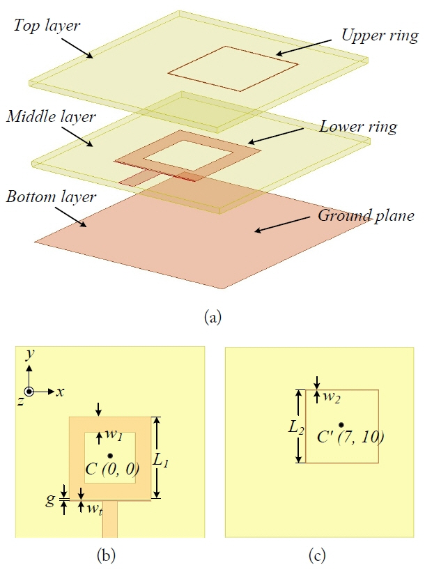
Fig. 1 shows the proposed dual-band CP antenna on a double-layer. The dielectric constant ɛr = 2.2 and thickness h = 1.574 mm of the two substrates are used for the proposed design. The size of substrate_2 is same with that of substrate_1. The ground plane size is 70 mm × 70 mm.
The proposed antenna consists of two square rings and a T-shaped feed line. The two (lower and upper) square rings have the outer side length of L1 and L2 and widths of w1 and w2. A lower ring is located on the middle layer and an upper ring is located on the top layer. These rings serve as radiating elements. Here, the center position of the lower ring is established as a reference point. It is denoted by C(0, 0). The center position of the upper square ring moves from (0, 0) to 7 mm on the x-axis and 10 mm on the y-axis. It is denoted by C′(7, 10). The width wf of the feed line is chosen to be 4.2 mm, which corresponds to the characteristic impedance of 50 Ω. Simulation is carried out using IE3D (Mentor Graphics, Wilsonville, OR, USA).
III. Parameter Study
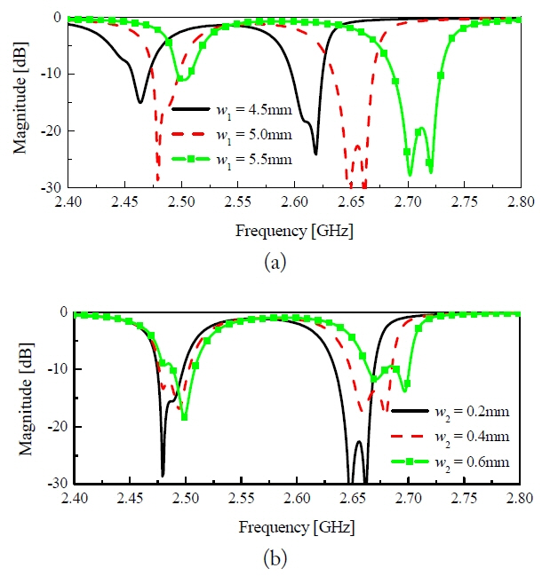
Fig. 2(a) and (b) show the simulated results of the proposed antenna for widths w1 and w2, respectively. The side lengths (L1 and L2) of the two square rings are 26 mm and 23.4 mm, respectively. The other parameters are: g = 0.2 mm and wt = 0.2 mm. It is well known that the resonant frequency of the ring resonator is mainly adjusted by changing the width of the ring. In this work, also, the lower ring works as a radiating element and works as a feed structure for the upper ring. Therefore, both resonant frequencies are increased as w1 increases. The proposed antenna shows good impedance matching at the upper band when w1 are all three values (4.5 mm, 5 mm, 5.5 mm) used above. It is observed that impedance matching has the optimum value as the width w1 = 5 mm. On the other hand, it can be observed from Fig. 2(b) that an increase in w2 increases the upper band. In this case, the lower band remains almost unchanged. Considering the impedance matching characteristic at both bands, the width w2 is fixed to 0.2 mm.
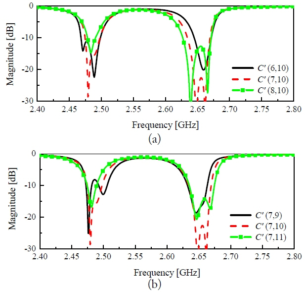
Fig. 3 shows the simulated results of the proposed antenna with different positions of the upper ring. In this case, the lower ring is fixed. The other dimensions are the same as before. When the upper ring shifts leftward (−x axis) or downward (−y axis), there is a greater split between the two degenerated modes at the lower band. On the other hand, the two degenerated modes at the upper band are more split when the upper ring shifts in the opposite direction (+x axis or +y axis). In the cases of C′(6, 10) and C′(7, 9), there is a single resonance at the upper band. Therefore, the proposed antenna exhibits a linear polarization (LP) property at the upper band. In cases of C′(8, 10) and C′(7, 11), the proposed antenna shows a single resonance at the lower band. Therefore, the proposed antenna has LP operation at the lower band. With position C′ chosen to be (7, 10), CP performance has the optimum value in this study.
IV. Simulated and Measured Results
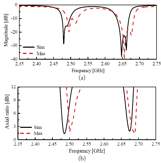
The proposed antenna is designed and fabricated with optimal parameters and measured to confirm the simulation performance. Detailed geometrical parameters of the optimal antenna are as follows: L1 = 26 mm, L2 = 23.4 mm, w1 = 5 mm, w2 = 0.2 mm, g = 0.2 mm, wt = 0.2 mm, and C′(7, 10). Fig. 4 exhibits both the simulated and measured reflection coefficient and axial-ratio (AR) for the proposed antenna. The proposed antenna features 10-dB impedance bandwidths of 1.3% and 1.7 % and 3-dB AR bandwidths of 0.7% and 0.8% in the lower and upper bands, respectively. The reason for the difference between measurement and simulation is due to the tiny air gap between the two substrates or the alignment between ring resonators in different layers.
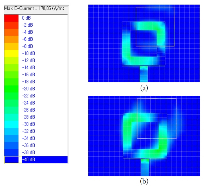
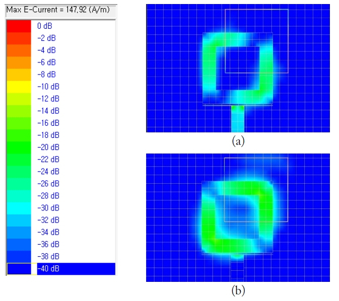
Figs. 5 and 6 show simulated current distributions at 2.482 GHz and 2.673 GHz, respectively. The blue and red areas indicate the minimum and maximum current distributions, respecttively. It can be seen from the current distribution that the proposed antenna operates as CP at two resonant frequencies.
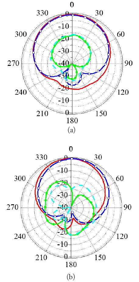
The radiation patterns measured at 2.5 GHz and 2.67 GHz are shown in Fig. 7. It can be found that the proposed antenna radiates a left-hand circularly polarized (LHCP) wave with cross polarization better than 15 dB for the lower and upper bands. The measured peak gains are about 4.2 dBi for the lower band and 4.6 dBi for the upper band.
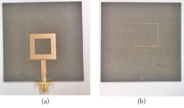
Fig. 8 shows the fabricated antenna.
V. Conclusion
The antenna structure consists of two square rings and a T-shaped feed line, and the proposed antenna exhibits CP operation because the relative distance between the two rings’ centers is used as a perturbation. A prototype of the proposed design has been successfully implemented. If a wireless communication system requires a dual-band CP property with a unidirectional radiation pattern, the proposed antenna is an option that can be considered because it has a simple configuration and is easy to manufacture.