J. Electromagn. Eng. Sci Search

CLOSE


J. Electromagn. Eng. Sci > Volume 20(1); 2020 > Article
Chaudhary and Jeong: Reconfigurable Negative Group Delay Circuit with a Low Insertion Loss Using a Coupled Line

Abstract

This paper presents a design of a transmissive-type, low insertion loss (IL) negative group delay (NGD) circuit with a reconfigurable NGD. The proposed circuit consists of a series transmission lines (TLs) and shunt short-circuited coupled lines where an isolation port is terminated with a parasitic compensated PIN diode. Analytical design equations are derived to obtain the circuit parameters for the predefined NGD and IL. The low IL can be achieved because of the very high characteristic impedance of the short-circuited coupled lines. The TL terminated with a PIN diode is used to achieve the constant center frequency of reconfigurable NGD circuit. For experimental validation, the NGD circuit is designed and fabricated at a center frequency (f0) of 2.14 GHz. In the measurement, the NGD varies from −0.5 ns to −2 ns with an IL variation of 2.08 to 3.60 dB at f0 = 2.14 GHz. The NGD bandwidth (bandwidth of GD less than 0 ns) varies from 90 MHz to 50 MHz. The minimum input/output return losses are higher than 10 dB for the overall tuning range.

I. Introduction

The propagation of electromagnetic waves in dispersive media can be characterized by abnormal phases, group delays, and velocities [1, 2]. In a specific frequency band of an anomalous dispersion, the abnormal group delay velocity is observed to be greater than the speed of light in vacuum or even a negative value [3]; this occurrence is defined as superluminal group velocity or negative group delay (NGD). NGD and NGD velocity are associated with each other. That is, the peak of the pulse envelope emerges from the medium at an instant before the peak of the pulse enters the medium.
Such a seemingly anti-causal phenomenon does not violate the principle of causality as the turn-on and turn-off points of the wave packet propagate with a positive delay in agreement with the causality requirements [4]. Theoretical and experimental investigations in the fields of electronic and microwave engineering have confirmed that different active and passive circuit topologies can generate the NGD phenomenon [513]. Moreover, researchers have been trying to find applications for NGD or the superluminal effect in various electronic circuits including enhancing the efficiency of a feed-forward amplifier, shortening delay lines, realizing non-Foster reactive elements, and minimizing beam-squint problems in series-fed antenna array systems [1317].
As NGD can be generated within a limited frequency band under a signal attenuation condition, various RLC resonator-based NGD circuits have been presented in the literature [69]. However, these conventional circuits have a fixed NGD. Efforts have been made to design a reflective-type reconfigurable NGD circuit using a 3-dB hybrid and RLC resonator [1820], which suffers from high insertion loss (IL). The IL in these works can be improved by increasing the characteristic impedance of the resonators and decreasing the value of R for the required NGD. However, the improvement of IL is limited because practically, implementing a high characteristic impedance (>130 Ω) microstrip line in PCB technology is difficult. A transmissive-type reconfigurable NGD circuit based on an open radial stub patch and a short-circuited stub with PIN diode is presented in [20]. To make a symmetrical structure, two units of NGD circuits are cascaded back to back, which increasing overall size and IL.
In this paper, a transmissive-type reconfigurable NGD circuit with low IL is demonstrated using a short-circuited coupled line and a PIN diode. Analytical design equations are derived to obtain the predefined NGD and IL.

II. Analytical Analysis

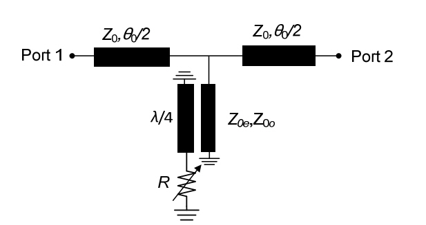
Fig. 1 shows the proposed structure of the reconfigurable NGD circuit, which consists of series transmission lines (TLs) and a shunt short-circuited coupled line where the isolation port is terminated with a variable resistor R. The characteristic impedance and electrical length of the series TLs are denoted as Z0 and θ0/2, respectively. The even- and odd-mode impedances of the coupled line are represented as Z0e and Z0o, respectively. Z0e and Z0o are expressed in terms of the characteristic impedance Zc and the coupling coefficient C of the short-circuited coupled line as (1).
(1a)
Z0e=ZcC1-C
(1b)
Z0o=ZcC1+C.
Using circuit theory, the overall S-parameters of the proposed circuit are derived as (2).
(2a)
S11=Z0(x1-jx2)x3-jx4e-jθ0ff0
(2b)
S21=2ZcC(ZcC-jRcotπf2f0)x3-jx4e-jθ0ff0,
where
(3a)
x1=R(C2csc2πf2f0-cot2πf2f0)
(3b)
x2=ZcCcotπf2f0
(3c)
x3=C2(2Zc2+Z0Rcsc2πf2f0)-Z0Rcot2πf2f0
(3d)
x4=Zc(Z0C+2RC)cotπf2f0
Moreover, f and f0 are the operating and design center frequencies, respectively. Using the phase of S21, the group delay (GD) of the proposed circuit can be derived as (4).
(4)
τ21=12π{θ0f0-RZcCcsc2πf2f02f0(Zc2C2+R2cot2πf2f0)-x3x4-x3x4x32+x42},
where
(5a)
x3=πf0Z0R(1-C2)cotπf2f0csc2πf2f0
(5b)
x4=-π2f0ZcC(Z0+2R)csc2πf2f0.
Finally, the S-parameters and GD at f = f0 of the proposed circuit are simplified as (6).
(6a)
S11|f=f0=RZ02Zc2+Z0R,
(6b)
S12|f=f0=2Zc22Zc2+Z0R
(6c)
τ21|f=f0=12f0{θ0π-R2ZcC+Zc(Z0+2R)2C(2Zc2+Z0R)}
From (6c), the proposed circuit can generate NGD (GD < 0 ns) if R is given as (7).
(7)
R>ZcZ0θ0C+ZcZ02θ02C2+πZ0(4θ0CZc+πZ0)πZ0
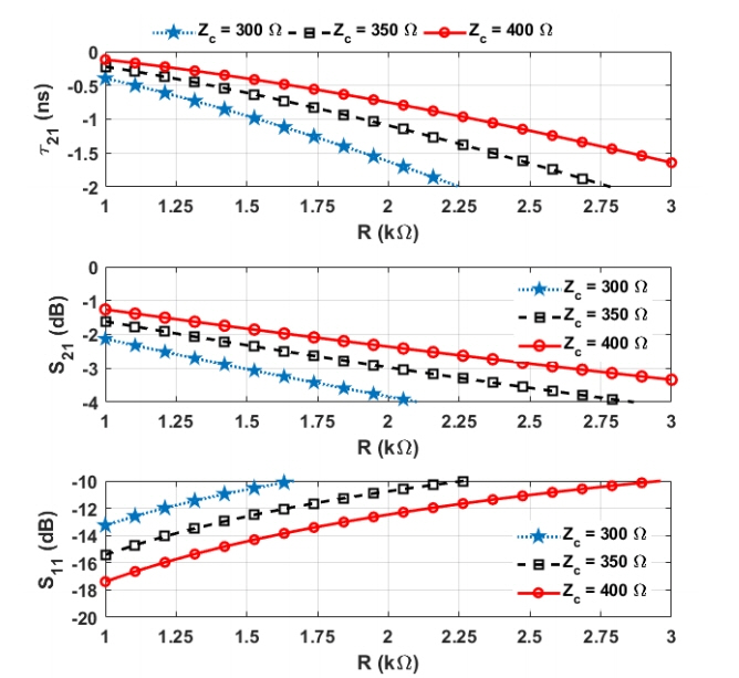
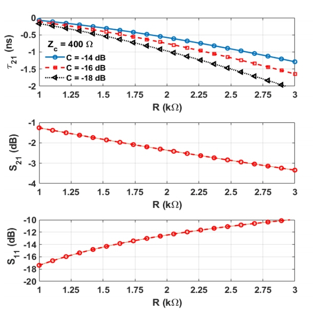
To validate the analysis, the calculated circuit parameters of the proposed reconfigurable NGD circuit are shown in Fig. 2 with different Zc and R. As observed in Fig. 2, the NGD and IL increased as R increases. Moreover, the proposed circuit can provide a low IL with the same NGD tuning range with high Zc, but the range of R is high for the same NGD. Fig. 3 shows the calculated NGD, IL, and input/output return losses according to the coupling coefficient (C) of the coupled line. As shown in Fig. 3, a higher NGD with the same IL and input/output return losses can be achieved by decreasing C.
Fig. 4 shows the calculated S-parameters and GD response of the proposed circuit. As shown in Fig. 4, the NGD is reconfigured from −0.5 ns to −2 ns at f0 = 2.14 GHz when R is changed from 1.50 kΩ to 2.91 kΩ. The IL and input/output return losses vary from 1.829 dB to 3.27 dB and 14.43 to 10.6 dB at f0 = 2.14 GHz, respectively.
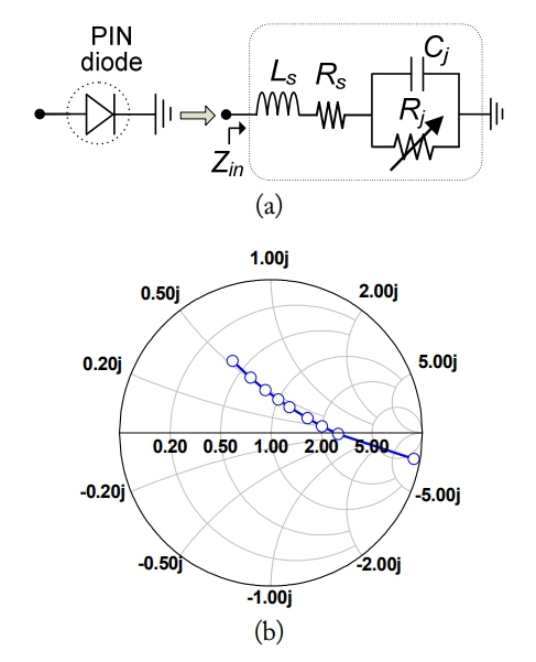
To implement the proposed reconfigurable NGD circuit, R should be applied with the PIN diode, which functions as a current-controlled variable resistor at microwave frequencies. In this work, the PIN diode HSMP-4810 from Avago was used. Fig. 5(a) shows the equivalent circuit model of the PIN diode. The input impedance of the PIN diode HSMP-4810 is not purely resistance as shown in Fig. 5(b), because of the parasitic components, which degrade the NGD performance of the reconfigurable NGD circuit at f0.
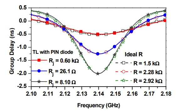
To obtain reconfigurable NGD results consistent with the analytical circuit analysis, the parasitic components of the PIN diode is compensated using TL (Z1, θ1) as shown in Fig. 6 [18]. To validate the proposed parasitic compensation method, the input impedances of the short-circuited coupled line with the ideal R and TL terminated with the PIN diode are shown in Fig. 7. As shown in the figures, the imaginary part of the input impedances (Fig. 6) at f0 = 2.14 GHz are maintained at around zero, and reconfigurable real part of the input impedances is the same as the short-circuited couple line terminated with the ideal R.
Fig. 8 shows the GD responses of the proposed reconfigurable NGD circuit with the ideal R and parasitic compensated PIN diode. The GD of the parasitic compensated PIN diode is almost the same as the analytical calculated results using (4).

III. Simulation and Measurement

For experimental validation, the proposed circuit is designed, fabricated, and measured at f0 = 2.14 GHz using the substrate RT/duroid 5880 with a dielectric constant of 2.2 and thickness of 0.787 mm. The goals are to achieve the GD variation of −0.5 ns to −2 ns and input/output return losses higher than 10 dB at f0. Based on the above design specification, the calculated circuit parameters are determined as Zc = 400 Ω, C = −17 dB, Z0e = 65.80 Ω, Z0o = 49.51 Ω, θ0 = 70o, Z0 = 50 Ω, and R = 1.57 to 3.14 kΩ. The physical layout with the dimensions and a photograph of the fabricated circuit are shown Fig. 9.
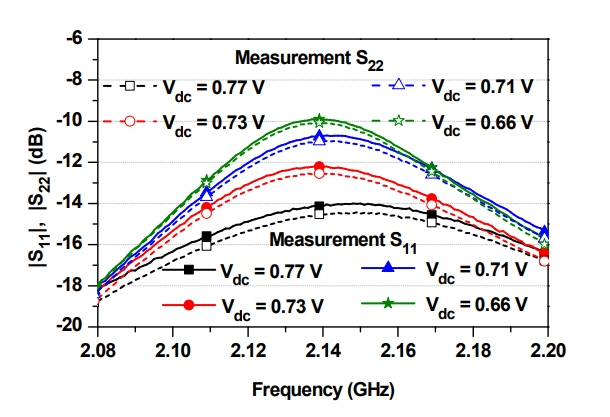
Fig. 10 illustrates the simulated and measured GD and |S21| results. The measurement results agreed well with the simulation results. From the measurement, the GD is reconfigured from −0.49 ns to −2.02 ns with an IL variation of 2.08 to 3.60 dB at f0 = 2.14 GHz when the bias voltage varies from 0.779 V to 0.66 V. The NGD bandwidths (bandwidth of GD < 0 ns) are achieved from 90 MHz to 50 MHz for the overall tuning range of GD. Fig. 11 shows the measured |S11| and |S22|, which vary from −14.12 to −10.01 dB for the overall GD range. Table 1 shows the performance comparison of the proposed circuit with the state-of-the-art. As shown in Table 1, the proposed work has an IL of 3.60 dB when the GD is equal to −2 ns. However, the ILs—28.60 dB in [18], 19.50 dB in [19], and 4.50 dB in [20]—are higher than that of the proposed work for the same GD (e.g., GD = −2 ns). Therefore, the proposed circuit provides a reconfigurable NGD with a low IL compared with the state-of-the-art [1820].

IV. Conclusion

This paper demonstrates a reconfigurable NGD circuit with a low IL using a coupled line and a parasitic compensated PIN diode. Both the analytical and experimental results validate the proposed circuit. To obtain consistent results with the analytical analysis, the parasitic components are compensated by using the TL terminated PIN diode. The measurement results agreed well with the analytically predicated and simulation results. The proposed circuit is expected to apply in various applications of microwave communication systems.

Acknowledgments

This work was supported by the Basic Science Research Program through the National Research Foundation of Korea (NRF) funded by the Ministry of Education (No. 2019R1A6A1A09031717).

Fig. 1
Proposed reconfigurable NGD circuit with low IL.
jees-20-1-73f1.jpg
Fig. 2
Calculated group delay, |S21|, and |S11| according to Zc and R with f0 = 2.14 GHz, C = −16 dB, and θ0 = 70°.
jees-20-1-73f2.jpg
Fig. 3
Calculated group delay, |S21|, and |S11| according to C and R with f0 = 2.14 GHz, Zc = 400 Ω, and θ0 = 70°.
jees-20-1-73f3.jpg
Fig. 4
Calculated S-parameters and GD with Zc = 400 Ω, C = −18 dB, and θ0/2 = 35°.
jees-20-1-73f4.jpg
Fig. 5
(a) Equivalent circuit model and (b) measured reflection coefficient of the PIN diode HSMP-4810 at f0 = 2.14 GHz. The parasitic components are Rs = 3 Ω, Ls = 1 nH, and Cj = 0.35 pF.
jees-20-1-73f5.jpg
Fig. 6
(a) A short-circuited coupled line terminated with the ideal R and (b) a parasitic compensated PIN diode with Rs = 3 Ω, Ls = 1 nH, and Cj = 0.35 pF.
jees-20-1-73f6.jpg
Fig. 7
Input impedance of a short-circuited coupled line terminated with the ideal R and a parasitic compensated PIN diode with Zc = 400 Ω, C = −18 dB, R1 = 1,480 Ω, Z1 = 120 Ω, and θ1 = 83.5°
jees-20-1-73f7.jpg
Fig. 8
Group delay with the ideal R and a parasitic compensated PIN diode with Zc = 400 Ω, C = −18 dB, R1 = 1,480 Ω, Z1 = 120 Ω, θ1 = 83.5°, Rs = 3 Ω, Ls = 1 nH, and Cj = 0.35 pF.
jees-20-1-73f8.jpg
Fig. 9
(a) Physical layout and (b) photograph of the fabricated reconfigurable NGD circuit. Physical dimensions: R1 = 1.5 kΩ, Cdc = 18 pF, L0 = 16, W0 = 2.4, Wc = 1.8, gc = 0.8, Lc = 25, W1 = 0.5, L1 = 3.7, L2 = 5.6, L3 = 3.70, L4 = 3, L5 = 4.4, and L6 = 6 (unit: mm).
jees-20-1-73f9.jpg
Fig. 10
Simulated and measured results of the proposed reconfigurable NGD circuit: (a) group delay and (b) |S21|.
jees-20-1-73f10.jpg
Fig. 11
Measured |S11| and |S22|.
jees-20-1-73f11.jpg
Table 1
Performances comparison of proposed NGD circuit with state-of-the-arts
Ref. f0 (GHz) GD (ns) IL (dB) NGD BW (MHz) A
[6] 0.45 −1.52 14.5* 103 N
[7] 2.14 −1.76 16 60 N
[8] 1.96 −6.5 21.20 200 N
[9] 1.96 −5.90 39.25 140 N
[18] 2.14 −2 to −20 28.6–46.1 80–40 Y
[19] 2.14 −2 to −20 19.5–41.5 80–40 Y
[20] 1.73 −2 to −10 4.50–9.30 40–30 Y
This work 2.14 −0.5 to −2.02 2.08–3.60 90–50 Y

A = NGD tenability, NGD BW = bandwidth of GD < 0 ns,

* active NGD circuit.

References

1. L Brillouin, Wave Propagation and Group Velocity. New York, NY: Academic Press, 1960.

2. EL Bolda, RY Chiao, and JC Garrison, "Two theorems for the group velocity in dispersive media," Physical Review A, vol. 48, no. 5, pp. 3890–3894, 1993.
crossref
3. AH Dorrah, L Kayili, and M Mojahedi, "Superluminal propagation and information transfer: a statistical approach in the microwave domain," Physics Letters A, vol. 378, no. 44, pp. 3218–3224, 2014.
crossref
4. CM Hymel, MH Skolnick, RA Stubbers, and ME Brandt, "Temporally advanced signal detection: a review of the technology and potential applications," IEEE Circuits and Systems Magazine, vol. 11, no. 3, pp. 10–25, 2011.
crossref
5. B Ravelo, A Perennec, M Le Roy, and YG Boucher, "Active microwave circuit with negative group delay," IEEE Microwave and Wireless Components Letters, vol. 17, no. 12, pp. 861–863, 2007.
crossref
6. M Kandic and GE Bridges, "Asymptotic limits of negative group delay in active resonator-based distributed circuits," IEEE Transactions on Circuits and Systems I: Regular Papers, vol. 58, no. 8, pp. 1727–1735, 2011.
crossref
7. H Choi, K Song, CD Kim, and Y Jeong, "Synthesis of negative group delay time circuit," In: Proceedings of 2008 Asia-Pacific Microwave Conference; Macau, China. 2008;pp 1–4.

8. G Chaudhary, Y Jeong, and J Lim, "Microstrip line negative group delay filters for microwave circuits," IEEE Transactions on Microwave Theory and Techniques, vol. 62, no. 2, pp. 234–243, 2014.
crossref
9. J Park, G Chaudhary, J Jeong, and Y Jeong, "Microwave negative group delay circuit: filter synthesis approach," Journal of Electromagnetic Engineering and Science, vol. 16, no. 1, pp. 7–12, 2016.
crossref pdf
10. G Chaudhary and Y Jeong, "Distributed transmission line negative group delay circuit with improved signal attenuation," IEEE Microwave and Wireless Components Letters, vol. 24, no. 1, pp. 20–22, 2013.
crossref
11. G Chaudhary, Y Jeong, and J Lim, "Miniaturized dualband negative group delay circuit using dual-plane defected structures," IEEE Microwave and Wireless Components Letters, vol. 24, no. 8, pp. 521–523, 2014.
crossref
12. G Chaudhary, J Jeong, P Kim, and Y Jeong, "Negative group delay circuit with improved signal attenuation and multiple pole characteristics," Journal of Electromagnetic Engineering and Science, vol. 15, no. 2, pp. 76–81, 2015.
crossref pdf
13. G Chaudhary and Y Jeong, "A design of compact wideband negative group delay network using cross coupling," Microwave and Optical Technology Letters, vol. 56, no. 11, pp. 2495–2497, 2014.
crossref
14. H Choi, Y Jeong, CD Kim, and JS Kenney, "Efficiency enhancement of feedforward amplifiers by employing a negative group-delay circuit," IEEE Transactions on Microwave Theory and Techniques, vol. 58, no. 5, pp. 1116–1125, 2010.
crossref
15. H Noto, K Yamauchi, M Nakayama, and Y Isota, "Negative group delay circuit for feed-forward amplifier," In: Proceedings of 2007 IEEE/MTT-S International Microwave Symposium; Honolulu, HI. 2007;pp 1103–1106.
crossref
16. H Mirzaei and GV Eleftheriades, "Realizing non-Foster reactive elements using negative-group-delay networks," IEEE Transactions on Microwave Theory and Techniques, vol. 61, no. 12, pp. 4322–4332, 2013.
crossref
17. H Mirzaei and GV Eleftheriades, "Arbitrary-angle squint-free beamforming in series-fed antenna arrays using non-Foster elements synthesized by negative-group-delay networks," IEEE Transactions on Antennas and Propagation, vol. 63, no. 5, pp. 1997–2010, 2015.
crossref
18. J Jeong, S Park, G Chaudhary, and Y Jeong, "Design of tunable negative group delay circuit for communication systems," In: Proceedings of 2012 IEEE International Symposium on Radio-Frequency Integration Technology (RFIT); Singapore. 2012;pp 59–61.
crossref
19. J Jeong, K Mok, J Kim, Y Jeong, and J Lim, "Negative group delay circuit with independently tunable center frequency and group delay," In: Proceedings of 2013 Asia-Pacific Microwave Conference Proceedings (APMC); Seoul, Korea. 2013;pp 197–199.
crossref
20. G Liu and J Xu, "Reconfigurable negative group delay circuit with low signal attenuation," Microwave and Optical Technology Letters, vol. 59, no. 10, pp. 2538–2542, 2017.
crossref

Biography

jees-20-1-73i1.jpg
Girdhari Chaudhary received his B.E. and M.Tech. degrees in electronics and communication Engineering from Nepal Engineering College (NEC), Kathmandu, Nepal and Malaviya National Institute of Technology (MNIT), Jaipur, India, in 2004 and 2007, respectively. He obtained his Ph.D. degree in electronics engineering from Jeonbuk National University, Republic of Korea in 2013. He is currently working as an assistant research professor in the Division of Electronics Engineering, Jeonbuk National University, Korea. He worked as the principal investigator (PI) of an independent project through the Basic Science Research Program of the National Research Foundation (NRF) funded by the Ministry of Education Korea. He is a recipient of the BK21 PLUS Research Excellence Award 2015 given by the Ministry of Education, Republic of Korea. Currently, he has received a Korean Research Fellowship (KRF) through the National Research Foundation (NRF) of Korea funded by the Ministry of Science and ICT. His research interests include multi-band tunable passive circuits, negative group delay circuits and its applications, in-band full duplex systems and high efficiency power amplifiers. Dr. Chaudhary served as reviewer for IEEE Transaction on Microwave Theory and Techniques, IEEE Microwave and Wireless Component Letters, IEEE Transaction on Circuit and Systems-I, and IEEE Transaction on Industrial Electronics.

Biography

jees-20-1-73i2.jpg
Yongchae Jeong received his B.S.E.E., M.S.E.E., and Ph.D. degrees in electronics engineering from Sogang University, Seoul, Republic of Korea in 1989, 1991, and 1996, respectively. From 1991 to 1998, he worked as a senior engineer in Samsung Electronics. In 1998, he joined the Division of Electronics Engineering, Jeonbuk National University, Jeonju, Republic of Korea. From July 2006 to December 2007, he joined at the Georgia Institute of Technology as a visiting professor. Currently, he is a professor, member of the IT Convergence Research Center, and director of HOPE-IT Human Resource Development Center of BK21 PLUS in Jeonbuk National University. He teaches and conducts research in the areas of microwave passive and active circuits, mobile and satellite base-station RF systems, design of periodic defected transmission line, and RFIC design. Dr. Jeong is a senior member of IEEE and a member of the Korea Institute of Electromagnetic Engineering and Science (KIEES). He has authored and co-authored over 200 papers in international journals and conference proceedings.

ABOUT
ARTICLE CATEGORY

Browse all articles >

BROWSE ARTICLES
AUTHOR INFORMATION
Editorial Office
#706 Totoo Valley, 217 Saechang-ro, Yongsan-gu, Seoul 04376, Korea
Tel: +82-2-337-9666    Fax: +82-2-6390-7550    E-mail: admin-jees@kiees.or.kr                

Copyright © 2024 by The Korean Institute of Electromagnetic Engineering and Science.

Developed in M2PI

Close layer
prev next