I. Introduction
Recently, high-intensity nanosecond pulsed electric field (PEF) has attracted significant research attention in the fields of biomedical engineering, food processing, and high-power electromagnetic (HPEM) effect testing. Interactions between PEF and biological objects have been investigated for potential applications, such as cancer therapy, cell death, and fast wounded healing [1ŌĆō3]. Some techniques and electrical analyses have been proposed through PEF experiments [4ŌĆō6]. Picosecond PEF was applied for the selective electroporation of organelles [7]. A non-invasive PEF technique was introduced for industrial food processing [8]. Furthermore, numerous studies have been conducted on the generation and radiation of intensive PEF for HPEM effect testing of electric devices [9ŌĆō12].
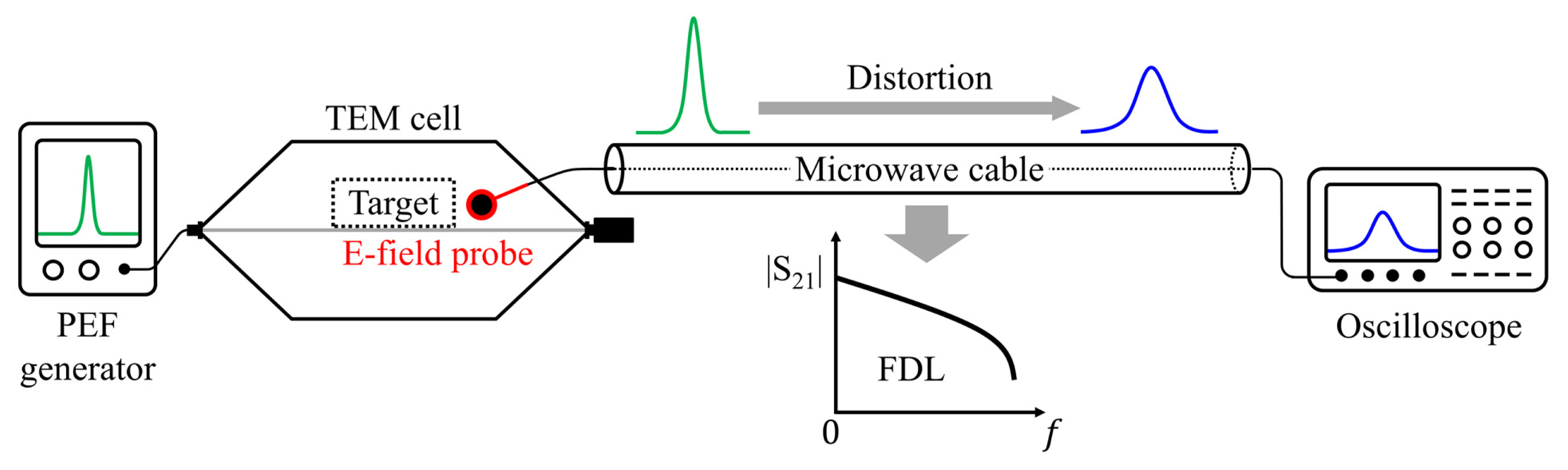
In PEF effect tests, it is important to accurately measure the PEF waveforms delivered to the targets. A PEF waveform is measured by an instrument, such as an electric field probe [4] or a capacitive voltage divider [13], and then the measured PEF is transferred to an oscilloscope through a microwave cable. In this measurement, the microwave cable is essential for several reasons. If the oscilloscope is installed close to the probe without a microwave cable, the PEF distribution near the field probe can not only be distorted by the field reflected from the oscilloscope but the PEF can also damage the oscilloscope.
In general, the loss of the microwave cable tends to increase with the signal frequency. Moreover, the group delay of the microwave cable varies with the signal frequency [14]. With this frequency-dependent loss (FDL), the pulse waveform passing through the microwave cable is distorted in the PEF measurement. For this reason, pulse waveform correction is required to obtain precise experimental results in PEF effect testing by using an appropriate transmission-line transfer function to recover the PEF waveform.
Scattering parameters have been extensively measured and exploited to characterize microwave networks or material parameters [15, 16], to validate the performance of microwave devices [17ŌĆō19], and to design a matching circuit between two ports [20].
Furthermore, several studies have been done to characterize and remove the effect of a system or fixture between external ports. The time-domain input and output waveforms of an overall system were measured to achieve a transfer function using a deconvolution method with parameter tuning [21ŌĆō24]. A de-embedding method was used to extract the design parameters of an antenna system or to present the S-parameters of a fixture [25, 26].
However, the deconvolution method cannot be applied to the time-domain PEF waveform correction because both input and output time-domain waveforms are measured to determine the transfer function of a system, but only the output pulse waveform of the microwave cable can be measured in PEF effect testing. In addition, the de-embedding method has rarely been investigated for the reconstruction of time-domain waveforms.
For this reason, we propose a new correction method to recover the output pulse distorted by a microwave cable. Here, the correction method employs a transfer function that can compute an input signal from an output signal in transmission line circuits. Here, the transfer function is first represented by the ABCD parameters of the microwave cable, and then the ABCD parameters are represented by the scattering parameters of the microwave cable, where the scattering parameters are measured using a vector network analyzer (VNA).
As a result, the transfer function used to calculate the undistorted input pulse from the distorted output pulse is expressed as a function of the measurable scattering parameters of the microwave cable. An RG-213 cable of length 10 m is tested to verify the proposed correction method, where the input pulse is a 2-ns sine pulse of a single cycle. By using the proposed correction method, the pulse amplitude and pulse width errors decrease dramatically in the PEF waveform measurement. In Section II, we present the process used to derive the transfer function for the proposed correction. In Section III, we validate the proposed method through measurement and computation. In Section IV, we apply the correction method to various pulse widths, pulse types, and cable types, and then discuss the correction results. Finally, Section V concludes this study.
II. Proposed Correction Method
Fig. 1 shows the experimental setup for PEF effect testing. A PEF generator transmits a PEF through a transverse electromagnetic (TEM) cell. The PEF delivered to the target is measured by an electric field probe. As mentioned in Section I, a microwave cable should be installed between the oscilloscope and electric field probe in the PEF measurement to prevent the PEF distribution from being distorted by the oscilloscope and to protect the oscilloscope from being damaged by the PEF. Here, the electrical properties of the microwave cable are maintained constant in the PEF experiments because the power strength handled by the microwave cable in the experiments is low enough considering that the E-field probe has, in general, a very small coupling coefficient. Moreover, the group delay of the microwave cable varies slightly for the measuring bandwidth. Therefore, the microwave cable in this experimental setup can be modeled as a linear time-invariant system. However, because the microwave cable incurs inevitable FDL, it distorts the PEF waveform in the measurement.
For a more precise acquisition of PEF waveforms, we propose a correction method to recover the distorted pulse waveform. Here, we denote the input and output pulses of the microwave cable as v1(t) and v2(t), respectively. We express them in the frequency domain by applying FFT, as follows:
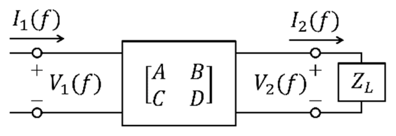
In the PEF test configuration, the microwave cable equipped between the oscilloscope and electric field probe has a transmission property represented by the ABCD parameters, as shown in Fig. 2. Using these parameters, we can obtain the transfer function of the microwave cable in the frequency domain, which is expressed as
Here, the input pulse is given by
where
Because the scattering parameters of the microwave cable can be measured using a VNA to present the ABCD parameters, we denote A and B in the scattering parameters as follows [27]:
where
is the ratio of the reflected voltage amplitude
V i - V j +
where
represents the oscilloscope input impedance in a PEF measurement setup, where
S 11 o s c
Therefore, the corrected pulse in the frequency domain can be determined by multiplying the transfer function with the output pulse in the frequency domain (i.e., HV2(f)). This corrected pulse is then converted to a time-domain pulse by conducting an inverse fast Fourier transform (IFFT) on HV2(f) as follows:
Through these processes, we can correct the PEF waveforms distorted by the FDL of the microwave cable.
III. Measurement and Computation
As described in the previous section, the output pulse of a microwave cable can be corrected using the proposed correction method. In this section, we validate the correction method by using time-domain pulse measurement, scattering parameter measurement, cable resistance measurement, and computation using MATLAB.
1. Measurement Setup
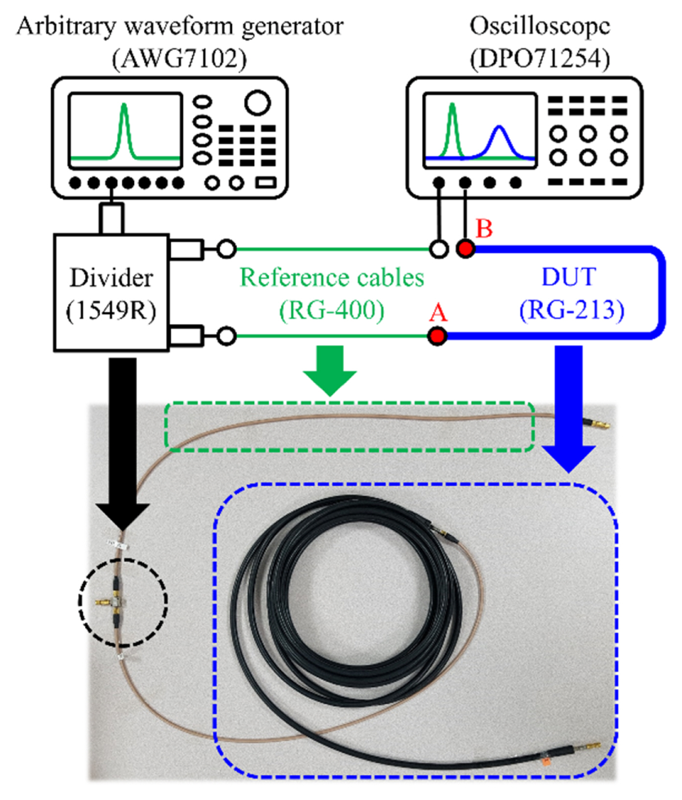
Fig. 3 shows the time-domain measurement setup for validating the correction method. An arbitrary waveform generator (Tektronix AWG7102, 10 GS/s) generates a single sine pulse with a pulse duration of 2 ns. Then, the pulse is equally divided into two microwave channels by using a resistive divider (Weinschel 1549R). One divided pulse goes through a reference cable (1 m of RG-400) and is measured by the first channel of the oscilloscope (Tektronix DPO71254, 50 GS/s). This pulse is called the reference pulse. Here, 1 m of RG-400 is used as the reference cable because it has a very low loss in the bandwidth of the pulses used for the validation. The other divided pulse is delivered through another reference cable and the device under test (DUT) cable (RG-213, 10 m). Then, it is measured by the second channel of the oscilloscope. The pulse before entering the DUT is called the input pulse. The pulse measured on the second channel is called the output pulse. The oscilloscope acquires 5,000 samples over 100 ns for each measurement, and each frequency spectrum of the measured pulses has 2,500 points from 0 Hz to 25 GHz after an FFT is applied.
We use a VNA (Keysight N9918A) to measure the DUT and oscilloscope channel scattering parameters of 1601 points ranging from 10 MHz to 16.01 GHz, so the frequency points of the scattering parameters align with the points of each frequency spectrum of the pulses with an equal frequency step of 10 MHz.
Additionally, a resolution bandwidth of 10 Hz is employed to ensure precise measurement. In Fig. 3, the reference planes for the scattering parametersŌĆÖ measurement are points A and B, which are the input and output ports of the DUT, respectively.
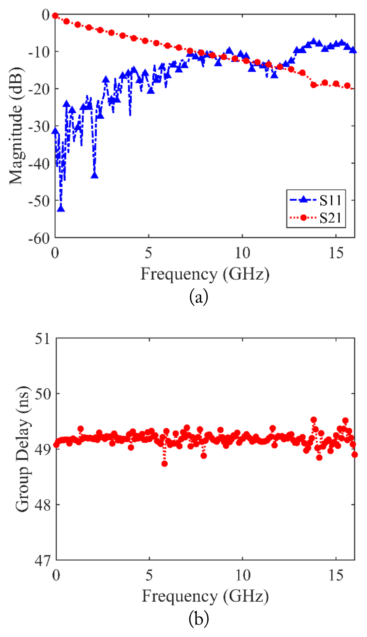
The real and imaginary parts of the scattering parameters are extracted so that they can be readily used in the computation. Then, the scattering parameters can be expressed as SMN = SMNr + jSMNi, where M, N are 1 or 2 in a two-port network, and SMNr and SMNi are the real and imaginary parts of SMN, respectively. Fig. 4(a) shows the magnitudes of S11 and S21 of the DUT, and Fig. 4(b) shows the group delay of S21 of the DUT. We can observe that the loss of the microwave cable varies with frequency, while its group delay changes slightly with frequency.
Fig. 5(a) shows the extracted S11r and S11i. In addition, Fig. 5(b) presents the measurement results of S21r and S21i. In the proposed correction method, the transfer function in Eq. (8) should cover dc, but the network analyzer cannot measure the dc scattering parameters. The dc transfer function is calculated by
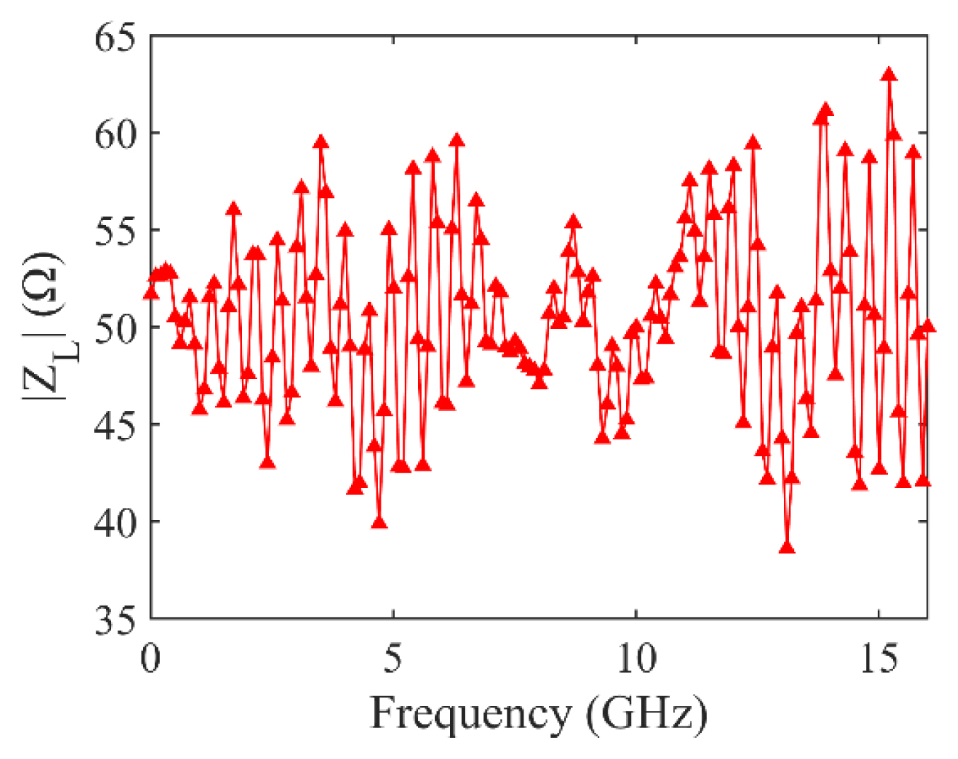
where Rcable is the dc resistance of the cable and ZL (f=0) is the dc oscilloscope input impedance. Fig. 6 shows the magnitude of the measured oscilloscope input impedance. All measurement results are loaded by the MATLAB code to correct the distorted output pulse.
2. Correction Results
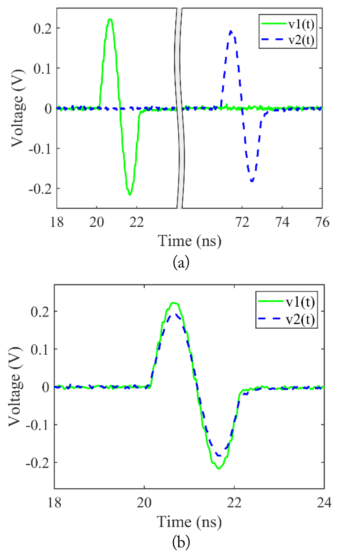
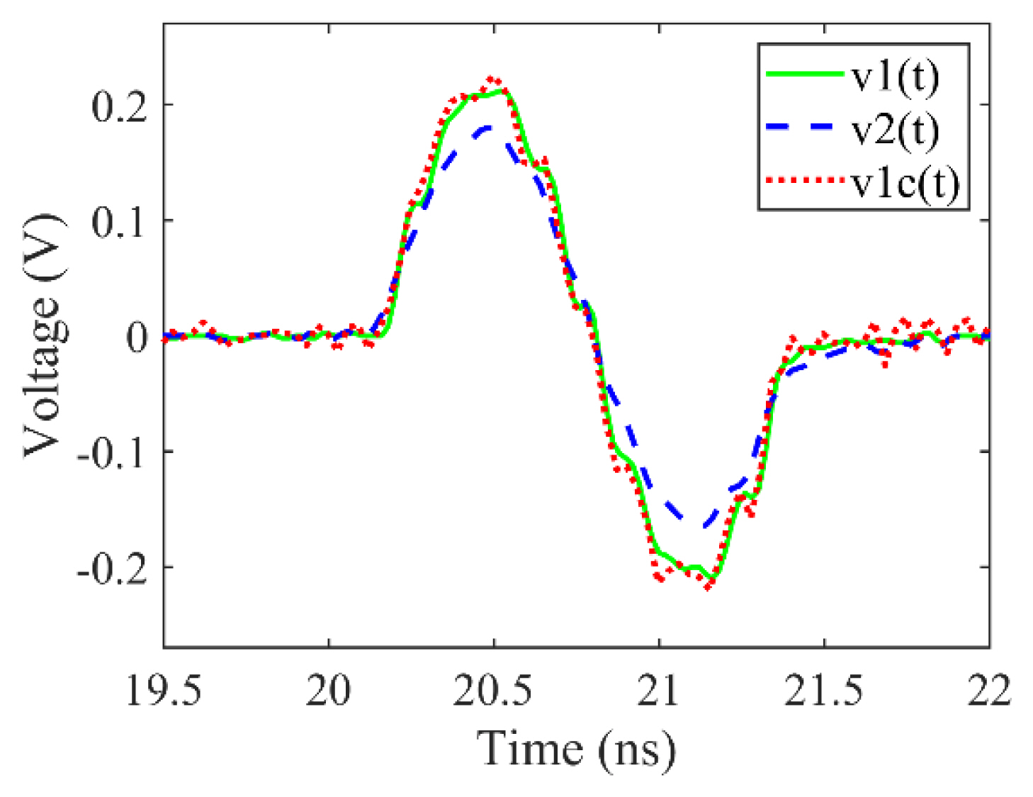
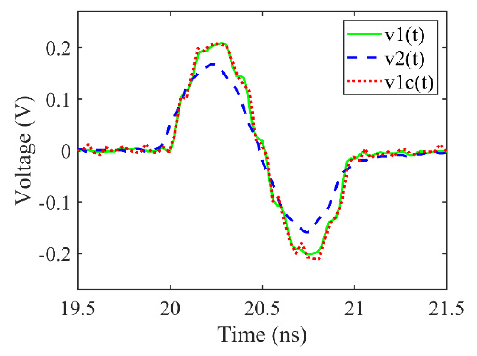
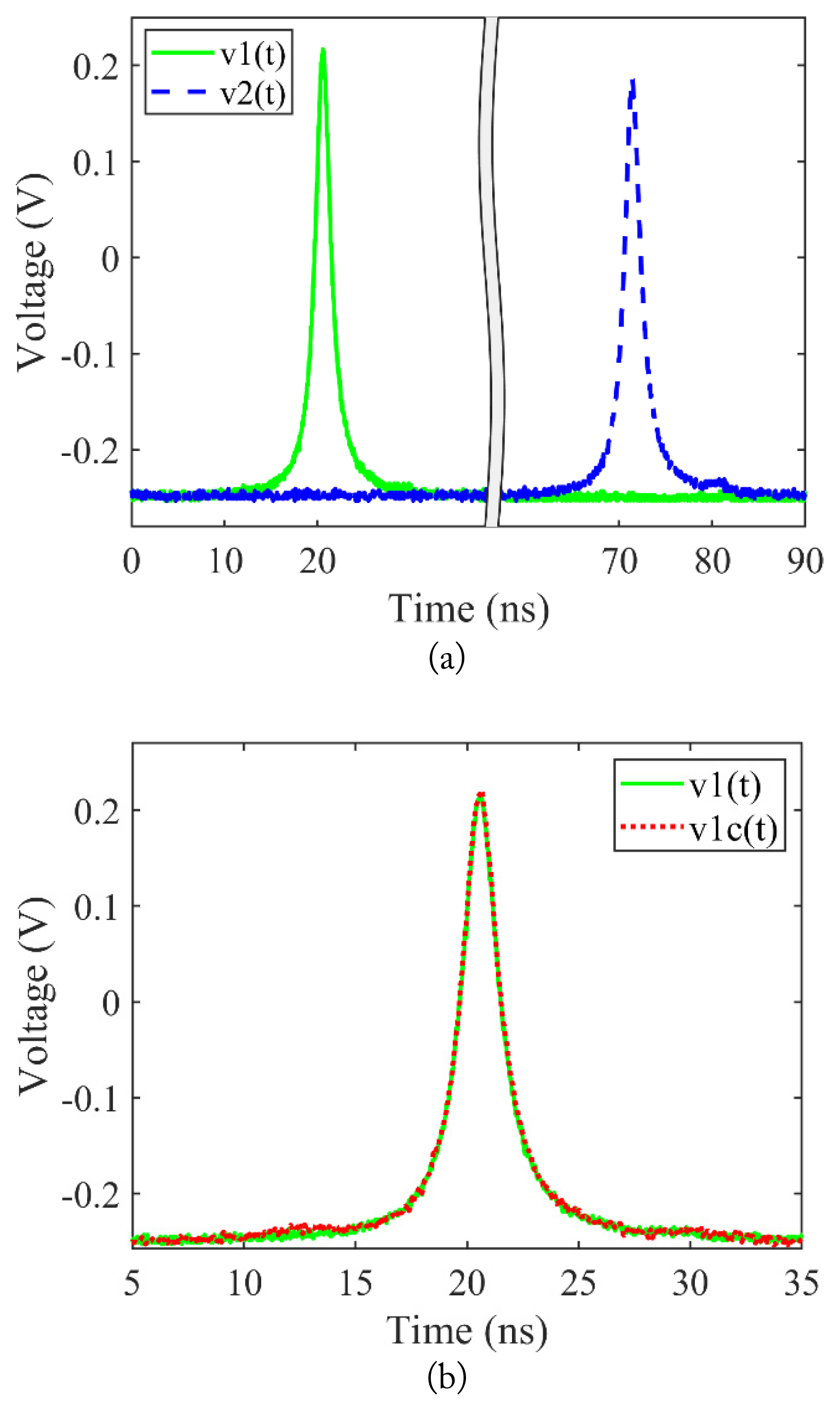
The proposed correction method is tested for an RG-213 microwave cable of length 10 m by using the experimental setup shown in Fig. 3. Fig. 7(a) shows the reference pulse v1(t) and output pulse v2(t), which are measured by the oscilloscope. Here, the total time for the pulse measurement is 100 ns. The time difference between the two pulses is approximately 40 ns, and the amplitude of the output pulse is notably smaller than that of the reference pulse. For a clearer comparison of the two pulses, Fig. 7(b) illustrates v1(t) overlapped by v2(t).
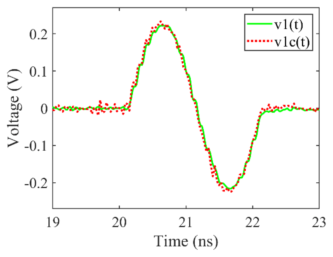
Fig. 8 illustrates the reference pulse v1(t) and the corrected pulse v1c(t) recovered by the proposed correction method. Here, we define two figures-of-merit to quantitatively compare the output pulse and the corrected pulse with the reference pulse. These figures-of-merit are percent amplitude error (PAE) and percent pulse-width error (PPWE), which are represented by
respectively, where the peak-to-peak voltages of the corrected pulse and reference pulse are
V p p c o r r V p p r e f
Table 1 lists the correction results in detail; and demonstrates that PAE is reduced from 14.6% to 4.5%, and PPWE is reduced from 10.4% to 0.8%. Moreover, the reference pulse and corrected pulse nearly overlap for the displayed time range, as shown in Fig. 8. Therefore, the proposed method is sufficient for correcting the PEF waveforms distorted by the FDL of the microwave cable in PEF effect experiments.
IV. Discussion
In the previous section, the correction method was validated for a 2-ns bipolar pulse. To ensure that the correction method can be used in more general PEF applications, the correction method must be verified under various conditions. For this reason, the correction method is tested for various pulse widths, pulse types, and cable types.
1. Correction of Pulses with Various Pulse Widths
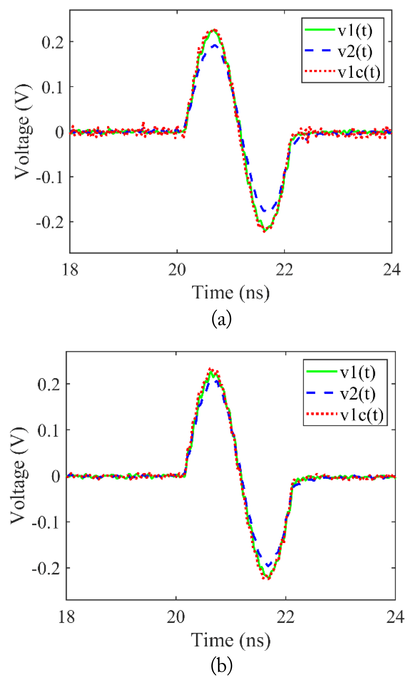
The correction method must be verified for various pulse widths, because PEF, in practice, can have various pulse widths. Because a narrower pulse has more high-frequency components, the distortion of the pulse waveform increases as the pulse width narrows. Therefore, we compare the test results obtained for a 2-ns single sine pulse with those obtained for 1.3- and 1-ns single sine pulses.
Figs. 9 and 10 show the waveforms of the reference pulse v1(t), output pulse v2(t), and corrected pulse v1c(t) for 1.3- and 1-ns pulses, respectively. Table 1 lists the test results, including those of 2-ns pulse. The measurement and computation processes are the same as those mentioned in Section III.
As shown in Table 1, the PAE for the 1.3-ns pulse decreases from 18.5% to 5.3%, and the PPWE for the 1.3-ns pulse decreases from 10% to 0.8%. The PAE for the 1-ns pulse decreases from 20.5% to 2.1%, and the PPWE for the 1-ns pulse decreases from 17.0% to 1.0%. Here, compared to the correction results obtained for the 2-ns pulse, the 1.3-ns and 1-ns pulses have larger errors in pulse amplitude and width measurement, but the errors for the corrected waveforms of 1.3-ns and 1-ns pulses are similar to those of the 2-ns pulse. As shown in Figs. 9 and 10, the overall waveforms of the corrected pulses are almost identical to the reference pulse waveforms.
2. Correction of a Unipolar Pulse
The correction method also needs to be tested for the unipolar pulse, not only for the bipolar pulse, because a unipolar pulse is widely used in many PEF effect tests. Here, a Lorentzian function is denoted as
where
is adopted to apply the proposed correction method to a unipolar pulse. Here, we use the same RG-213 cable and the same process as that mentioned in Section III.
Fig. 11 presents the waveforms of the reference pulse v1(t), output pulse v2(t), and corrected pulse v1c(t) for the unipolar pulse. Fig. 11(a) shows the reference pulse and distorted output pulse. As shown in Fig. 11(b), the overall shape of the corrected pulse overlaps with the reference pulse with a little difference.
According to Table 2, with the use of the correction method, the PAE of the unipolar pulse declines from 6.4% to 1.8%, and the PPWE decreases from 16.8% to 1.9%. Here, the PAE of the unipolar pulse is calculated as
where the amplitudes of the corrected pulse and reference pulse are
V p c o r r V p r e f
3. Pulse Correction for Various Cable Types
There are many types of microwave cables that transmit the PEF signal from the electric-field sensor to the measuring oscilloscope. To validate the correction method for different types of cables, we apply the proposed method to RG-8 and LMR-400 cables, and then the test results are compared with those of RG-213 described in Section III. All test conditions and computation processes are the same as those used for the RG-213 cable. The length of each cable is 10 m.
Fig. 12(a) presents the waveforms of the reference pulse v1(t), output pulse v2(t), and corrected pulse v1c(t) for RG-8. According to Table 3, the PAE of RG-8 is reduced from 16.6% to 1.4%, and the PPWE is reduced from 8.4% to 0.3%. Fig. 12(b) shows the correction result for LMR-400. As shown in Table 3, the PAE of LMR-400 is reduced from 9.8% to 2.3%, and the PPWE is reduced from 4.2% to 2.3%. These results validate the proposed correction method for PEF measurement for the different cable types.
V. Conclusion
This paper proposes a correction method to recover the pulse waveforms distorted by the FDL of a microwave cable. The correction method is obtained by building a transfer function using the ABCD parameters obtained from the scattering parameters of the microwave cable. The correction method is validated by measurement and computation. The time-domain output pulse, frequency-domain scattering parameters, and cable resistance are measured to build the transfer function for the correction. Then, the correction method is implemented in MATLAB code, and the measurement results are loaded to compare the corrected pulse with the reference pulse. The correction method is successfully validated for a DUT cable with a 2-ns input pulse of a sine shape because the PAE is reduced from 14.6% to 2.4% and the PPWE is reduced from 10.4% to 0.8%. In addition, the correction method is verified for various pulse durations, pulse types, and cable types.
The correction method is prepared for application to the measurement of PEF waveforms delivered to targets in PEF effect testing. The proposed correction method can be applied not only to correct PEF waveforms distorted by a microwave cable but also by other microwave devices that have the FDL, such as attenuators, baluns, and couplers.