I. Introduction
With the recent advancements in device technology, systems operating at a frequency exceeding 100 GHz are being widely studied for various high-frequency applications, including imaging and communication [1, 2]. One of the difficulties in designing such a system is the presence of unwanted parasitic components that critically affect the system performance [3]. Therefore, given such an effect, we can expect the performance of designed circuits to be significantly affected by the layout of the circuits. In this study, we investigated the actual effect of layout on the circuit performance of two 110-GHz oscillators fabricated in Samsung 65-nm CMOS technology.
II. Circuit Design
To study the effect of layout on circuit performance, we designed and implemented two LC cross-coupled oscillators (OCS1 and OCS2) with different layout schemes. Fig. 1 shows the schematic of the oscillator design, which is identical for the two oscillators on the circuit level. The LC cross-coupled oscillator is composed of four transistors, two (M1 and M2) for the oscillator core and the other two (M3 and M4) for the buffer.
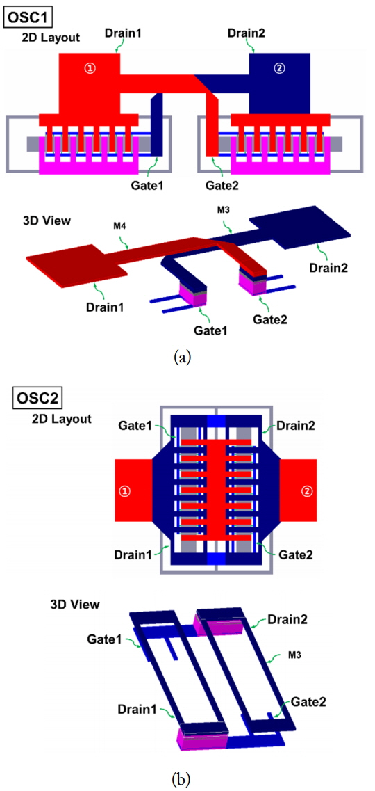
Based on the schematic design, we drew two different core layouts, which are expected to critically affect the oscillators’ electrical performances. The layout details of the two core drawings are depicted in Fig. 2. For the core of OSC1, as shown in Fig. 2(a), the cross-coupled lines are placed outside the device area, which is the conventional approach. For the implementation, since a line crossing is inevitable, two metal layers of M3 and M4 are used to interconnect the gate and the drain of the other device. For the core of OSC2, as shown in Fig. 2(b), the cross-coupled lines are formed inside the device area. This case takes advantage of the symmetry in the layout of the offered transistors in a process design kit (PDK) and uses a single metal layer M3 for the cross-coupling. Such a modification is expected to improve the circuit performance.
First, as in [4], for an LC cross-coupled oscillator, wOSC can be obtained as follows:
From (1), we can see that by reducing LF, higher oscillation frequency, wOSC, can be obtained for OSC2. Second, since the cross-coupled metal length is reduced, parasitic resistance, Rp, will also reduce, which will lead to enhancement of the resonator’s Q-factor. The enhancement in Q-factor, in turn, will increase the output power. Lastly, as shown in Fig. 2(b), perfect symmetry can be obtained as a single metal layer is used for cross-coupling, providing advantages of a fully differential pair for OSC2.
III. Measurement Results
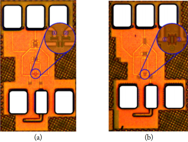
The two 110-GHz oscillators were fabricated with Samsung 65-nm CMOS process, which has fT/fmax = 200/220 GHz. The chip photos for the fabricated oscillators are shown in Fig. 3. Each oscillator occupies an area of 540 μm × 320 μm, including probing pads for DC supply and RF measurements.
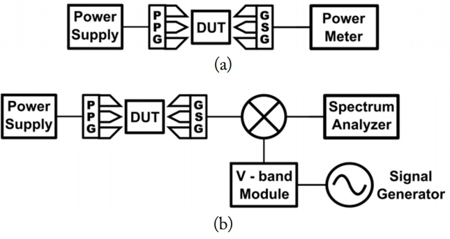
The electrical performances were characterized by measuring the output power, spectrum, and phase noise. The measurement setups are described in Fig. 4. For the power measurement, a VDI PM5 power meter was directly connected to the DUT via a GGB D-band GSG probe. For the spectrum and phase noise measurement, a VDI WR6.5 subharmonic mixer, an Agilent V-band source module, an Agilent E8247C signal generator, and an Agilent E4440A spectrum analyzer were used.
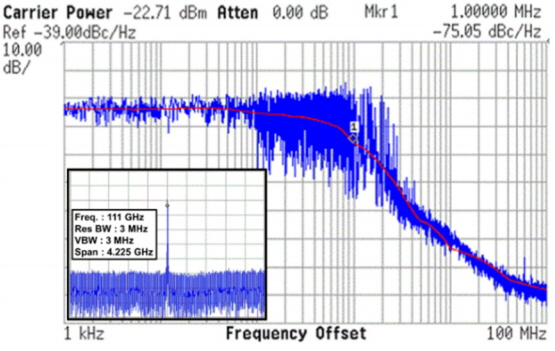
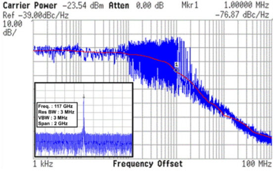
OSC1 generated an output power of −3.9 dBm at 111 GHz and showed a phase noise of −75 dBc/Hz at 1-MHz offset. The results are shown in Fig. 5. OSC2 generated an output power of −2 dBm at 117 GHz and a phase noise of −77 dBc/Hz at 1-MHz offset. The results are shown in Fig. 6. The output power values were calibrated with a probe loss of 2.5 dB (from data sheet). Table 1 shows the summarized oscillator performances. The results clearly indicate that the modified layout with improved symmetry and reduced coupling metal line length leads to enhancement in both output power and phase noise.
IV. Conclusion
Two LC cross-coupled oscillators fabricated in Samsung 65-nm CMOS technology were developed and compared. The oscillator with a modified layout (OSC2) showed enhanced performance compared with the conventional layout (OSC1). The improvement is ascribed to improved symmetry as well as reduced inductance and parasitic line resistance.