J. Electromagn. Eng. Sci Search

CLOSE


J. Electromagn. Eng. Sci > Volume 19(1); 2019 > Article
Yoon and Kim: Modified Wilkinson Power Divider Using Transmission Lines for Various Terminated Impedances and an Arbitrary Power Ratio

Abstract

This paper introduces a modified Wilkinson power divider that uses uniform transmission lines for various terminated impedances and an arbitrary power ratio. For the designed power ratio, the proposed divider changes only the electrical lengths of the transmission lines between the input and output ports, and those between the output ports and the isolation resistor. In this case, even when various termination impedances of the ports exist, the divider characteristics are satisfied. To verify the feasibility of the proposed divider, two circuits were designed to operate at a frequency of 2 GHz with 2:1 and 4:1 power splitting ratios and various terminated impedances of 40, 70, and 60 Ω for one circuit, and 50, 70, and 60 Ω for the other. The measurement and simulation results were in good agreement.

I. Introduction

The divider is the most widely used passive component in the wireless industry. In many cases, the same splitting divider is used [1, 2]. However, in special applications, cases that require unequal distribution [3, 4] or various termination impedances [5, 6] exist. To achieve a divider with unequal or various terminated impedances, a high-impedance transmission line must be implemented. Such a high-impedance transmission line is difficult to implement because of its very narrow line width that must be implemented through microstrip technology. Moreover, to satisfy the characteristics of the high-impedance line, a bulky capacitor or coupled lines with narrow gaps are used.
Recently, a new design method has been proposed to adjust only the electrical length of the transmission lines between the input and output ports, or between the output ports and the isolation resistor, to achieve the operation of an unequal divider. Many dividers using a uniform transmission line have been introduced, such as a divider with uniform transmission lines of various electrical lengths [79], a structure using an isolated resistor with open-stub connection to obtain enhanced bandwidth [10], an isolated resistor configuration connected to the same impedance lines between the output ports with long stub length [11], a structure connected to various impedance lines at both sides of an isolation resistor [12], a Gysel divider with a phase shifter instead of a 180° transmission line [13], a ring hybrid coupler with a 50-Ω transmission line [14], and a half mode substrate integrated waveguide (HMSIW) divider with composite right and left-handed transmission line (CRLH-TL) [15]. This type of splitter uses a transmission line with uniform impedance, and it does not use an impedance transformer to match each port, even though it operates as an unequal divider. Such a divider consists of circuits with an arbitrary power split ratio and a termination impedance of 50 Ω.
In this paper, we propose a modified Wilkinson divider using a uniform transmission line with various termination impedances and an arbitrary dividing ratio as well as the previously used 50 Ω termination impedance. This type of device eliminates the requirement for a matching circuit between the divider and the peripheral device with various termination impedances, and allows a small circuit size to be achieved.

II. Theory and Design

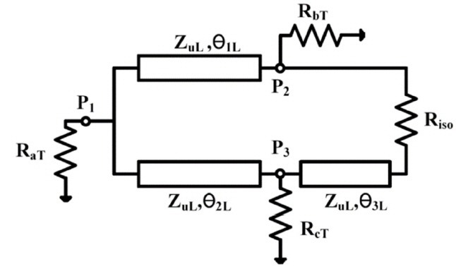
Fig. 1 shows the schematic of the proposed power divider with power splitting ratio k2 (= P2/P3). This proposed divider consists of three transmission lines with uniform impedance ZuL and various electrical lengths of θ1L, θ2L, and θ3L, an isolation resistor Riso, and various terminated impedances of RaT, RbT, and RcT.
In addition, this divider must satisfy the S-parameter characteristics of the unequal Wilkinson power divider:
(1)
(S)unequal=11+k2(0k·e-jβe-jβk·e-jβ00e-jβ00)
where β is the phase shift of the transmission coefficient.
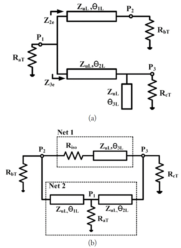
Because the proposed power divider with various terminated impedances is asymmetrical, we analyzed it using scattering parameters rather than the conventional even-odd method. When port 1 is excited, all power is transmitted to the output ports, P2 and P3, and the voltage from the branch of P1P2 to ground is the same as that from the branch of P1P3 to ground at any distance from P1, and no current flows in the isolation resistor. Because the isolation resistor operates as an open circuit, we can design an equivalent circuit between ports 2 and 3, as shown in Fig. 2(a). The ABCD parameters between port 1 and ports 2 and 3 can be expressed as
(2)
(A21B21C21D21)=(cos θ1LjZuL·sin θ1Ljsin θ1LZuLcos θ1L)
(3)
(A31B31C31D31)=(cos θ2LjZuL·sin θ2Ljsin θ2LZuLcos θ2L)(10jtan θ3LZuL1)
The ABCD parameters of Eqs. (2) and (3) can be converted into the S-parameters of S21 and S31. Using the relation of S21 =k·S31, the following related equations are then obtained.
(4)
k2RcTRbT·(RbT+1+k2k2RaT)cos θ1L={RcT+(1+k2)RaT}cos θ2L-RcTsin θ2Ltanθ3L
(5)
k2RcTRbT·(ZuL2+1+k2k2RaTRbT)sin θ1L={ZuL2+(1+k2)RaTRcT}sin θ2L+(1+k2)RaTRcTcos θ2Ltan θ3L
In Fig. 2(a), under the input matching condition (S11 = 0), we have
(6)
1Z2e+1Z3e=1RaT
(7)
Z2e=ZuLRbT+jZuLtanθ1LZuL+jRbTtanθ1L
(8)
Z3e=ZuLRcT(1-tan θ2Ltan θ3L)+jZuLtan θ2LZuL+jRcT(tan θ2L+tan θ3L)
where Z2e and Z3e are the input impedances of the upper and lower branches, respectively.
Based on the principle of conservation of energy and ideal transmission lines, the real parts of Z2e and Z3e are expressed as follows:
(9)
Re[Z2e]=1+k2k2RaT
(10)
Re[Z3e]=(1+k2)RaT
In Fig. 2(b), when port 2 is excited, the networks of Net1 and Net2 are connected in parallel, in which Net1 consists of the isolation resistor Riso and the transmission line of electrical length θ3L; and Net2 consists of a termination resistor RaT and transmission lines of electrical lengths θ1L, θ2L. The ABCD parameters of Net1 and Net2 can be expressed as:
(11)
(ANet1BNet1CNet1DNet1)=(1Riso01)(cos θ3LjZuLsin θ3Ljsin θ3LZuLcos θ3L)
(12)
(ANet2BNet2CNet2DNet2)=(cos θ1LjZuLsin θ1Ljsin θ1LZuLcos θ1L)(101RaT1)(cos θ2LjZuLsin θ2Ljsin θ2LZuLcos θ2L)
The ABCD parameters of Eqs. (11) and (12) are converted into the Y-parameters of Net1 and Net2, respectively, and the admittance parameters of the entire network can be obtained as follows:
(13)
(y11_toty12_toty21_toty22_tot)=(y11_Net1y12_Net1y21_Net1y22_Net1)+(y11_Net2y12_Net2y21_Net2y22_Net2)
where
  • y11_tot=cos θ3LRisocos θ3L+jZuLsin θ3L+cos θ1Lcos θ2L-sin θ1Lsin θ2L+jZuLRaTsin θ2Lcos θ1L-ZuL2RaTsin θ1Lsin θ2L+jZuL(sin θ2Lcos θ1L+sin θ1Lcos θ2L),

  • y12_tot=y21_tot=-1Risocos θ3L+jZuLsin θ3L+-1-ZuL2RaTsin θ1Lsin θ2L+jZuL(sinθ2Lcos θ1L+sin θ1Lcos θ2L),

  • y22_tot=cos θ3L+jRisoZuLsin θ3LRisocos θ3L+jZuLsin θ3L+cos θ1Lcos θ2L-sin θ1Lsin θ2L+jZuLRaTsin θ1Lcos θ2L-ZuL2RaTsin θ1Lsin θ2L+jZuL(sin θ2Lcos θ1L+sin θ1Lcos θ2L).

The admittance parameters of Eq. (13) can be converted to the S-parameters of S22, S32, and S33 with terminated impedances of RbT and RcT. The S-parameters of the entire network between ports 2 and 3 can be expressed as
(14)
S22=-(y11_tot-1RbT)(y22_tot+1RcT)-y12_tot·y21_tot(y11_tot+1RbT)(y22_tot+1RcT)-y12_tot·y21_tot
(15)
S32=-21RbT·1RcT·y21_tot(y11_tot+1RbT)(y22_tot+1RcT)-y12_tot·y21_tot
(16)
S33=-(y11_tot+1RbT)(y22_tot-1RcT)-y12_tot·y21_tot(y11_tot+1RbT)(y22_tot+1RcT)-y12_tot·y21_tot
Based on Eqs. (4) to (5), (9) to (10), and (14) to (16), the electrical lengths θ1L, θ2L, θ3L, and isolation resistance Riso that satisfy the power divider characteristic conditions with |S22| < −20 dB, |S33| < −20 dB, and |S32| < −20 dB at center frequency can be obtained by using MATLAB.

III. Simulation and Experimental Results

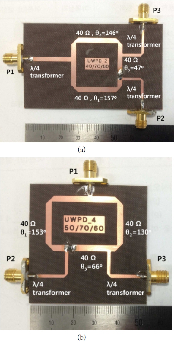
To validate the proposed power divider, we designed two types of circuits at a center frequency of 2 GHz. One has a power dividing ratio of k2 = 2 and port impedances of RaT = 40 Ω, RbT = 70 Ω, and RcT = 60 Ω. The second circuit has a power dividing ratio of k2 = 4 and port impedances of RaT = 50 Ω, RbT = 70 Ω, and RcT = 60 Ω. For the first circuit, when the transmission line characteristic impedance of ZuL = 40 Ω was chosen, we calculated the electrical lengths and isolation resistance using the equations above and after optimization as follows: θ1L = 157o, θ2L = 146o, θ3L = 47o, and Riso = 12 Ω. For the second circuit, when a transmission line characteristic impedance of ZuL = 40 Ω was chosen, we calculated the electrical lengths and isolation resistance using the equations above and after optimization as follows: θ1L = 153°, θ2L = 130°, θ3L = 66°, and Riso = 20 Ω. The Teflon substrate of the proposed power divider had a dielectric constant of 2.5, a thickness of 0.787 mm, and a conductor thickness of 0.035 mm.
The simulation was performed using Microwave Office software with version 13 developed by National Instruments.
Fig. 3(a) and (b) show the photographs of the circuits in which k2 = 2 and k2 = 4, respectively, where power dividers of various port impedances and uniform transmission lines are implemented. For the measurement, the impedance transformers shown in Fig. 3 were used to match the input and output ports to 50 Ω.
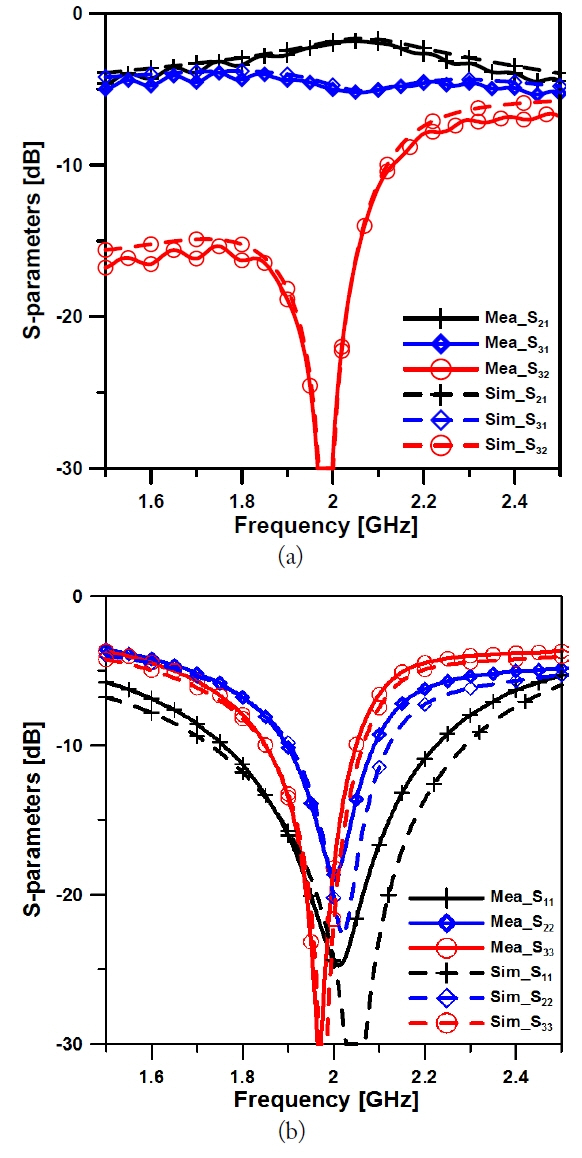
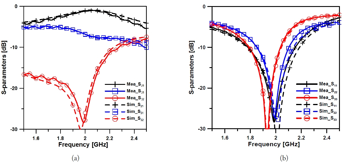
Fig. 4(a) and (b) show the measured and simulated S-parameters of the circuit with a power dividing ratio of k2 = 2 and port impedances of 40, 70, and 60 Ω; the figures show insertion losses of |S21| = 2.0 dB and |S31| = 5.0 dB, an isolation of |S32| > 25 dB, an input return loss of |S11| that is better than −20 dB, and output return losses of |S22|, |S33| that are better than −18 dB at the center frequency of 2 GHz. In addition, Fig. 5(a) and (b) show the measured and simulated S-parameters of the circuit with a power dividing ratio of k2 = 4 and port impedances of 50, 70, and 60 Ω; the figures show insertion losses of |S21| = 1.2 dB and |S31| = 6.8 dB, an isolation of |S32| > 25 dB, an input return loss of |S11| that is better than −25 dB, and output return losses of |S22|, |S33| that are better than −25 dB, −13 dB, respectively, at the center frequency of 2 GHz. In Figs. 4 and 5, the |S33| data can be observed with slight frequency deviation, which is caused by the parallel admittance of electrical length θ3L. Fig. 6 shows that the phase difference between the output ports of the k2 = 2 circuit is +3° at the center frequency of 2 GHz. Table 1 shows a comparison of dividers using the conventional uniform transmission line and the results obtained for the proposed divider. In addition, Table 2 summarizes the experimental results and design parameters of the proposed power divider.

IV. Conclusion

This paper presented a modified Wilkinson divider using uniform transmission lines for various terminated impedances and an arbitrary dividing ratio. With this configuration, the desired splitting ratio can be obtained by adjusting only the electrical length of the transmission lines between the ports. Moreover, it has the advantage that the impedance of the ports is set to various terminated impedances, and is connected to a circuit without a matching circuit. The feasibility of the proposed power divider design concept was demonstrated, and the simulated and measured results were confirmed to be in good agreement.

Fig. 1
Schematic of the proposed Wilkinson power divider.
jees-19-1-42f1.jpg
Fig. 2
(a) Equivalent circuit of proposed divider when port 1 is excited and (b) equivalent circuit of the proposed divider when port 2 is excited.
jees-19-1-42f2.jpg
Fig. 3
Photographs of the implemented power divider: (a) k2 = 2 and (b) k2 = 4.
jees-19-1-42f3.jpg
Fig. 4
Measured and simulated S-parameters of the k2 = 2 circuit: (a) |S21|, |S31|, |S32| and (b) |S11|, |S22|, |S33|.
jees-19-1-42f4.jpg
Fig. 5
Measured and simulated S-parameters of the k2 = 4 circuit: (a) |S21|, |S31|, |S32| and (b) |S11|, |S22|, |S33|.
jees-19-1-42f5.jpg
Fig. 6
Measured and simulated phase difference between the output ports of the k2 = 2 circuit.
jees-19-1-42f6.jpg
Table 1
Comparison of the proposed divider with conventional power dividers
Ref. Dividing ratio and type Frequency (GHz) Total lengtha (°) TL impedance (Ω) Term. (Ω) IL (dB) RL (dB) Isolation (dB)
[7] 2:1 / 4:1 (WPD) 1 270 / 300 70.7 50 0.3 30 30
[10] 4:1 (WPD) 3 388 50 50 0.9 15 20
[11] 1:1 (WPD) 60/90 321.04 50 50 0.3 22 19
[12] 2:1 / 4:1 / 9:1 (WPD) 3 324.82 / 332.21 / 341.66 50 50 - 20 20
[13] 9:1 (Gysel) 1 219 70.7 50 0.2 20 29
[14] 9:1 (Ring) 1 378.6 50 50 0.4 25 40
This work 2:1 / 4:1 (WPD) 2 350 / 349 40 40/50 / 60/70 0.3 18 25

WPD = Wilkinson power divider, IL = insertion loss, RL = return loss.

a Without output matching transformer.

Table 2
Summary of experimental results and design parameters of the proposed power divider
Dividing ratio Term. (Ω) |S21| (dB) |S31| (dB) |S11| (dB) |S22| (dB) |S33| (dB) |S32| (dB) θ1 (°) θ2 (°) θ3 (°) Riso (Ω)
2 40/70/60 2.0 5.0 −20 −18 −18 −25 157 146 47 12
4 50/70/60 1.2 6.8 −25 −25 −13 −25 153 130 66 20

REFERENCES

1. EJ Wilkinson, "An N-way hybrid power divider," IRE Transaction on Microwave Theory and Techniques, vol. 8, no. 1, pp. 116–118, 1960.
crossref
2. UH Gysel, "A new N-way power divider/combiner suitable for high-power application," In: Proceedings of IEEE MTT-S International Microwave Symposium; Palo Alto, CA. 1975;pp 116–118.

3. Y Kim and YC Yoon, "A modified unequal power divider with a complex isolation component for enhanced isolation," Microwave and Optical Technology Letters, vol. 57, no. 2, pp. 322–324, 2015.
crossref
4. AK Agrawal and GF Mikucki, "A printed circuit hybrid ring directional coupler for arbitrary power divisions," IEEE Transactions on Microwave Theory and Techniques, vol. 34, no. 12, pp. 1401–1407, 1986.
crossref
5. HR Ahn, I Wolff, and IS Chang, "Arbitrary termination impedances, arbitrary power division and small-sized ring hybrids," IEEE Transactions on Microwave Theory and Techniques, vol. 44, no. 12, pp. 2241–2247, 1997.

6. HR Ahn and I Wolff, "Three-port 3-dB power divider terminated by different impedances and its application to MMICs," IEEE Transactions on Microwave Theory and Techniques, vol. 47, no. 6, pp. 786–794, 1999.
crossref
7. KKM Cheng and PW Li, "A novel power-divider design with unequal power-dividing ratio and simple layout," IEEE Transactions on Microwave Theory and Techniques, vol. 57, no. 6, pp. 1589–1594, 2009.
crossref
8. PW Li and KKM Cheng, "A new unequal power-divider design with enhanced insertion loss flatness," IEEE Microwave and Wireless Components Letters, vol. 19, no. 12, pp. 786–788, 2009.
crossref
9. Z Haiwei and X Quan, "A novel Gysel power divider with arbitrary power ratio for high-power application," In: Proceedings of IEEE International Wireless Symposium (IWS); Beijing, China. 2013;pp 1–4.
crossref
10. YZ Zhu, XF Zhang, XF Wu, C Li, and GY Fang, "Novel Wilkinson power divider with uniform impedance line," In: Proceedings of Asia-Pacific Microwave Conference (APMC); Macau, China. 2008;pp 1–4.

11. S Horst, R Bairavasubramanian, MM Tentzeris, and J Papapolymerou, "Modified Wilkinson power dividers for millimeter-wave integrated circuits," IEEE Transactions on Microwave Theory and Techniques, vol. 55, no. 11, pp. 2439–2446, 2007.
crossref
12. T Qi, S He, Z Dai, and W Shi, "Novel unequal power divider with 50 Ω characteristic impedance lines," IEEE Microwave and Wireless Components Letters, vol. 26, no. 3, pp. 180–182, 2016.
crossref
13. F Lin, QX Chu, and SW Wong, "A novel Gysel power divider design with uniform impedance transmission lines for arbitrary power-dividing ratios," Journal of Electromagnetic Waves and Applications, vol. 27, no. 2, pp. 242–249, 2013.
crossref
14. MJ Park and B Lee, "Design of ring couplers for arbitrary power division with 50 Ω lines," IEEE Microwave and Wireless Components Letters, vol. 21, no. 4, pp. 185–187, 2011.
crossref
15. DS Eom and HY Lee, "A broadband half-mode substrate integrated waveguide quadrature Wilkinson power divider using composite right/left-handed transmission line," Journal of Electromagnetic Engineering and Science, vol. 17, no. 1, pp. 9–13, 2017.
crossref pdf

Biography

Young-Chul Yoon received his B.S., M.S., and Ph.D. in electronics engineering from Sogang University, Seoul, Korea, in 1978, 1982, and 1989, respectively. In 1987, he joined the Department of Electronics Engineering, Catholic Kwandong University, Gangneung, Korea, where he is currently a Professor. His areas of interest are the design of high power amplifiers for the ISM band, and RF and microwave circuit analysis and design.
jees-19-1-42i1.jpg

Biography

Young Kim received his B.S., M.S., and Ph.D. in electronics engineering from Sogang University, Seoul, Korea, in 1986, 1988, and 2002, respectively. He developed cellular and PCS linear power amplifiers at Samsung Electronics Co., Ltd. In 2003, he joined the School of Electronics Engineering, Kumoh National Institute of Technology, Gumi, Korea, where he is currently a Professor. His areas of interest are the design of high-power amplifiers and linearization techniques, and RF and microwave circuit analysis and design.
jees-19-1-42i2.jpg
TOOLS
Share :
Facebook Twitter Linked In Google+
METRICS Graph View
  • 3 Crossref
  • 4 Scopus
  • 5,702 View
  • 90 Download
Related articles in JEES

ABOUT
ARTICLE CATEGORY

Browse all articles >

BROWSE ARTICLES
AUTHOR INFORMATION
Editorial Office
#706 Totoo Valley, 217 Saechang-ro, Yongsan-gu, Seoul 04376, Korea
Tel: +82-2-337-9666    Fax: +82-2-6390-7550    E-mail: admin-jees@kiees.or.kr                

Copyright © 2024 by The Korean Institute of Electromagnetic Engineering and Science.

Developed in M2PI

Close layer
prev next