I. Introduction
A crossover coupler is an indispensable passive component in microwave systems. Specifically, a Butler matrix is an example of a beamforming network that requires a crossover coupler, as shown in Fig. 1. Array antennas are connected to the Butler matrix consisting of 3-dB quadrature hybrids, 45° phase shifters, and crossover couplers, so that the antenna beam is formed and steered electronically.
The crossover coupler makes two signals cross each other while maintaining a high degree of isolation. As the crossover coupler occupies a substantial area in the Butler matrix [1], size reduction is a critical issue in the coupler design.
Traditionally, the signal crossover was achieved by air-bridges or under-passes based on a multilayer printed circuit board (PCB) [2, 3]. However, those methods lead to non-planar structures, and increase the fabrication cost and difficulty. Thus, several fully planar configurations have been proposed for crossover applications [4â9]. A symmetrical four-port double-ring structure was reported in [4, 5]. A planar crossover was achieved by cascading two branch-line structures in [6]. The number of branch-line structures connected in cascade was increased to more than three in order to improve the operation bandwidth in [7].
However, most of the previous crossover couplers are bulky because they are based on quarter-wave transmission lines. To make the crossover smaller, a part of the transmission lines was shortened by connecting a shunted open stub at each end of the lines [8]. A dual-band crossover coupler was also proposed as a variation of the branch-line structure [9]. Nonetheless, all of these structures are still large and occupy a significant PCB area.
In this paper, a new compact wideband crossover coupler is presented. A three-section branch-line structure is employed for wideband operation. To reduce the size, all quarter-wave transmission lines are replaced by lumped components using the Ï- equivalent model. In Section II, a fully-lumped crossover coupler is proposed. In Section III, the coupler is designed at 2 GHz for the purpose of demonstration, followed by the experimental results given in Section IV.
II. Fully-Lumped Crossover Coupler
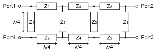
A conventional wideband crossover coupler based on a three-section branch-line structure [7] is shown in Fig. 2. The lengths of transmission lines are all quarter-wave, and the characteristic impedances are given by
where Z
c is the port impedance. Z
2 should be chosen considering the input matching and isolation performance, which was 40 Ω in [7]. However, the size of the conventional crossover coupler is large because all of the transmission lines are quarter-wave long. The electrical length of the lines are reduced by connecting the shunted open stubs in [8]. Nonetheless, the physical length of the lines is still large and becomes even larger as the operating frequency decreases.
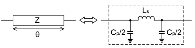
In this work, the quarter-wave transmission lines in Fig. 2 are replaced fully by lumped components. Therefore, the size of the crossover coupler is not only significantly reduced but also is independent of the operating frequency. Fig. 3 shows the Ï-equivalent lumped model of a transmission line. The values of the lumped components are given by [10],
where Z and Ξ are the characteristic impedance and electrical length of the transmission line, and f is the operation frequency.
Fig. 4(a) shows an initial version of the proposed lumped crossover coupler where each transmission line (Z
i
, 1 †i †4) is replaced by one inductor (L
i
) and two capacitors (C
i
/2). As the lines are quarter-wave long (Ξ = 90°), the lumped component values are derived from Eqs. (2) and (3):
where the characteristic impedance of the transmission lines, Z
i
, is given by Eq. (1).
To further reduce the coupler size of Fig. 4(a), two or three shunt capacitors connected at the same node are combined into a single capacitor. Finally, the complete schematic of the proposed fully-lumped crossover coupler is shown in Fig. 4(b). It consists of ten inductors and eight capacitors. The capacitor values are given by
III. Design of Fully-Lumped Crossover Coupler
A crossover coupler is designed at 2 GHz, following the proposed fully-lumped structure of Fig. 4(b). The lumped component values are theoretically calculated by Eqs. (1), (4), (6), and are summarized in the left column of Table 1. However, the theoretical values cannot be practically used for the coupler design and should be further optimized for two reasons.
Firstly, the component values available from commercial chip inductors and capacitors are limited. Thus, the values must be chosen from the set of discrete values available within the chip components.
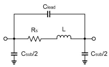
Secondly, the parasitics of the chip components must be considered for accurate simulation of the coupler performance. It was found that the chip inductors involve relatively large parasitics, so that their operation deviates considerably from those of ideal inductors. Therefore, the chip inductors on the PCB are measured by a network analyzer and then modeled using the equivalent circuit model [11] shown in Fig. 5. R
s
, C
lead
, and C
sub
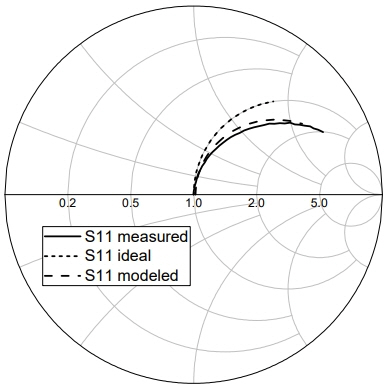
represent a parasitic series resistance, inter-lead capacitance, and substrate capacitance, respectively. Fig. 6 shows the measured Sparameters of a 3.9-nH chip inductor, compared with the simulation of an ideal inductor and the equivalent circuit model. It is observed that the equivalent circuit model predicts the measurement more accurately than the ideal inductor.
The values of the chip inductors and capacitors are optimized in simulation, while considering the two factors aforementioned: one is the discrete selection of commercial chip components and the other is the use of equivalent circuit model including parasitics. The optimized component values are given in the right column of Table 1.
IV. Experimental Results
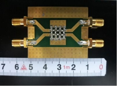
A 2-GHz crossover coupler was fabricated on an FR-4 PCB, which has a thickness of 1.6 mm, dielectric constant of 4.7, and loss tangent of 0.02 at 1 MHz. For chip components, WE-MK multilayer ceramic inductors with size of 0603 (1.6 mm Ă 0.8 mm) and Samsung multilayer ceramic capacitors with size of 0402 (1.0 mm Ă 0.5 mm) were used.
Fig. 7 shows the top view of the fabricated crossover coupler. The size of the crossover coupler (dashed box) is 11 mm à 9 mm, while 50-Ω feedlines are added to each port for the purpose of measurement. If normalized by wavelength, the size becomes 0.07λ à 0.06λ, which is significantly smaller than the conventional crossover couplers based on quarter-wave lines. For example, compared to the three-section branch-line [7] crossover coupler shown in Fig. 2, the size is reduced by 95%.
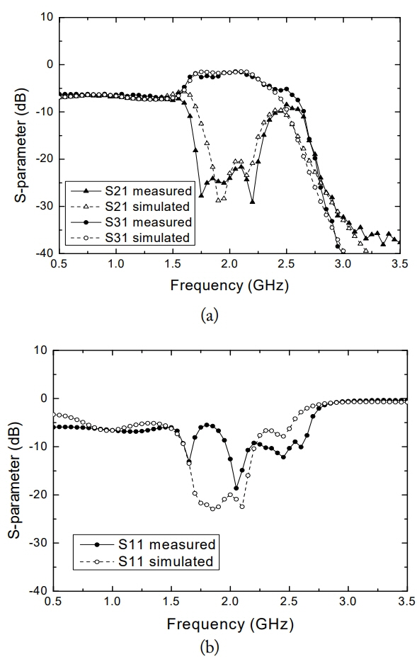
The measured S-parameters are shown in Fig. 8. The insertion loss, isolation, and return loss are 1.7 dB, 24 dB, and 14.5 dB, respectively, at 2 GHz. The fractional bandwidth achieving both 3-dB insertion loss and 20-dB isolation is 27% (from 1.71 to 2.25 GHz). A difference between the simulated and measured return loss is believed to be due to additional model inaccuracy of the lumped components, especially underestimation of capacitance of chip capacitors.
V. Conclusion
A compact and wideband crossover coupler is implemented using fully lumped components. For wideband operation, a three-section branch-line structure is employed. In order to reduce the size, the transmission lines are replaced by the Ï-equivalent lumped components. The measured fractional bandwidth for 3-dB insertion loss and 20-dB isolation is 27%, centered at 2 GHz. The size of the crossover coupler is only 0.07λ Ă 0.06λ. The performance comparison of the crossover coupler is given in Table 2. The proposed crossover coupler achieves a wide operating bandwidth with a size significantly smaller than others. It should be very suitable for Butler matrix requiring a compact form factor.