Design of a Ka Band Multi-Channel (25CH) Millimeter-Wave Downconverter for a Signal Intelligence System
Article information
Abstract
In this study, we propose an approach for the design and satisfy the requirements of the fabrication of a reliable and stable high-frequency downconverter for the millimeter-wave (Ka band) and detail the contents of the approach. We design and fabricate a stable downconverter with a low noise figure, flat gain characteristics, and multi-channel characteristics suitable for millimeter-wave bands. The method uses the chip-and-wire process for the assembly and operation of a bare MMIC device into the RF path. To compensate for the mismatch among the many components used in the module, W/G transition, an image rejection mixer, a switch, and an amplifier suitable for millimeter-wave frequency characteristics are designed and applied to the downconverter. To reject the spurious signals generated from the complex local oscillation signals, the downconverter is designed to not affect the RF path. In the Ka-band downconverter, the gain is measured from 41.89 dB to 42.83 dB at 33–35 GHz with flatness of about 0.94 dB. The measured value of the noise figure at CH1 is 4.936 dB with a maximum value in the 0.75–1.25 GHz intermediate frequency. The third intermodulation measurement result is 61.83 dBc under a −50 dBm input power and above gain, and the switching to select a channel takes about 622 μs.
I. Introduction
An aircraft signal intelligence (SIGINT) system is used strategically and tactically to gather signals from radars and communications systems. SIGINT systems are commonly divided into communications intelligence and electronic intelligence systems. As SIGINT systems require the ability to locate the source of enemy signals [1], direction finding (DF) to support this capability is an important requirement, and SIGINT systems generally operate in a wide frequency range of 20 MHz–40 GHz [2].
For electronic warfare (EW) requirements covering the Ka-band spectrum, a channelized receiver is highly desirable. The Future Combat Systems (FCS) radar and communications allocations exist in this band of the spectrum [3].
Broadband receivers with wide millimeter-wave bands are essentially required for electronic support systems. Millimeter-wave systems with at least 30 GHz millimeter-wave bandwidths with broad dynamic ranges, improved sensitivity, and front-end complexity are commonly required in the fields of communication, radar, and wireless communication. To satisfy such high requirements, general millimeter-wave systems include local oscillator (LO) and downconverter functions in their front-end receiver connected to an antenna. Moreover, the mixer, amplifier, and the many necessary components generally require multi-channels in which the frequencies have been converted into sub-octave bands to satisfy the system requirements because of their bandwidth and dynamic range limits. Channelized receivers divided into multiple channels can be optimized to satisfy the requirements of ESM receivers. The problems with this architecture include the fact that the multiplied local oscillation signals are fed back into the antenna path because of the low isolation between the RF and LO ports of the mixer and the reduced dynamic range due to the cascade structure that down–converts the frequencies [4–7].
Although numerous studies have been conducted to design millimeter-wave ultra-wideband receivers suitable for electronic support systems, many constraints remain on the design and manufacturing of such broadband downconverters. To make the receivers have low noise figures, flat gain characteristics in the band, wide dynamic ranges, and band-specific frequencies that can be selected with low-loss transmission lines, a local oscillator circuit necessary for frequency conversion should be incorporated in the module, and a closed structure is needed to avoid signal interference from other devices (IFF transponder, Doppler radar, communication system, etc.) in the system environment where the receivers are installed [8, 9].
In this paper, a design approach is proposed not only to improve the signal acquisition accuracy by maximizing the number of receiving input ports (25 input channels) but also to convert the signal frequencies of 33–35 GHz in the millimeter-wave Ka-band into the intermediate frequency (IF) 1 GHz (instantaneous frequency: 500 MHz) before the signals are delivered to the signal processing unit. The content of the design approach is as follows.
First, as the 33–35 GHz band received by an antenna through the free space medium has a waveguide structure, a transition structure should be designed to convert the channels into micro-strip transmission lines. To implement 25 channels in the form of grids in a limited space, the channels are designed using the Rogers RT/duroid 5880 5-mil PCB material for small insertion losses and better impedance matching.
Second, the signals are downconverted into IF signals with a center frequency of 1 GHz and a frequency band of 500 MHz through a low-noise amplifier (LNA) and a frequency converter (packaging type) including an image suppression function. At this time, the local oscillator signals necessary for frequency conversion are phase locked with the internal voltage-controlled oscillator (VCO) with an 8 GHz band using the external reference frequency of 1 GHz supplied by the system. As the voltage turning (VT) voltage of the VCO is high, the structure of the loop filter connected to the phase-locked loop (PLL) output terminal was designed as an active type instead of a passive type.
Third, as the RF lines must be designed considering the amplitude matching among multiple channels (25 channels), the RF lines of the individual channels are designed not only to be electrically the same but also to have the same component mounting positions and wire bonding length.
Fourth, to secure the degree of isolation between the input and output channels, the mechanism is designed to prevent signals from flowing into other channels using valley form equipment.
II. Millimeter-Wave Downconverter Structure
In this paper, a Ka-band multi-channel (25) millimeter-wave downconverter module mounted on the front-end terminal of an antenna is designed. This module has a complicated structure with 25 RF input (33–35 GHz) channels and 16 IF output (0.75–1.25 GHz) channels. The module is divided into module #1 and module #2 when it is mounted because of space restrictions for the entire system and to secure excellent noise figures. Module #1 is mounted near the antenna. A conceptual diagram of the entire system is shown in Fig. 1.
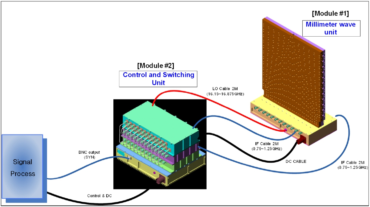
Configuration of the entire millimeter-wave downconverter.
Fig. 2 is a detailed block diagram of the multi-channel down-converter necessary for the SIGINT system. The multi-channel downconverter amplifies signals with a center frequency of 34 GHz (bandwidth 2 GHz) received from the antenna using an LNA and converts the amplified signals into IF signals with a center frequency of 1 GHz (RF bandwidth 2 GHz) through a frequency converter (MIXER), which includes an image suppression function. At this time, the local oscillator signals, which are necessary for frequency conversion having a frequency sweeping function with a 1 GHz bandwidth, are phase locked with the internal VCO with an 8 GHz band using the external reference frequency of 1 GHz supplied by the system, converted to have a 16 GHz band through a frequency doubler, and input into the LO port of the MIXER.
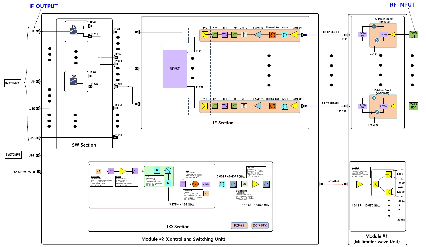
Detailed block diagram of the millimeter-wave downconverter.
The frequency converter (MIXER) is a component that contains a doubler inside, and the 16 GHz band is converted into a 32 GHz bandwidth inside the MIXER. In this case, the frequency converter has a frequency variable function, so that the local oscillator signals have a bandwidth of about 1.5 GHz (after multiplying).
III. Design and Simulation
1. W/G to M/S Line Transition Simulation
In most millimeter systems, the waveguide and the microstrip are the two commonly used transmission lines. The waveguide is usually employed to connect the antenna and the millimeter receiver or transmitter because of its low insertion loss [10]. To transmit signals in the super high 34 GHz frequency band from the waveguide (W/G) form to the micro-strip line structure, the electric field mode must be converted through a transition design.
As shown in Fig. 3(a), a transmission line with a single-layer structure was placed at a point of the height of the Lambda/4 (about 1.7 mm) of the center frequency from the bottom surface of the instrument of the W/G structure. For fine impedance matching, signals were simulated in the form of patches at the end of the transmission line, where the electric field is propagated. As shown in Fig. 3(b), the design results indicated the insertion loss was not larger than 0.1 dB and that the reflection coefficient was not larger than −23 dB in the 32–36 GHz band.
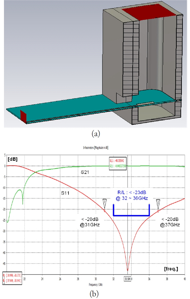
(a) Transition structure to convert the waveguide form into the micro-strip line. (b) Result of the transition simulation to convert the waveguide form into the micro-strip line.
To relieve the problems by comparing the design value and the actual measured value before installing on the module, a jig was fabricated to make back-to-back measurement possible using an Rogers RT/duroid 5880 PCB with permittivity of 2.2, as shown in Fig. 4(a). As a result of the measurement in Fig. 4(b), insertion losses not exceeding −1 dB and reflection coefficients not exceeding −13 dB were obtained. The reason why the measurement graph was wider by 1 GHz upward and downward from the band (33–35 GHz) was that the frequency drift was considered because of the errors that could occur in the actual fabrication.

(a) Photo of the evaluation jig to verify the transition structure. (b) Measurement results obtained with the evaluation jig.
2. PLL Design for the LO Section
To design the PLL local oscillation that is phase-synchronized with the external reference frequency, the external REF applied to the REF port of the PLLIC was injected after converting it into 200 MHz using a five-divider, and the LO frequency in the 16 GHz band was created in the VCO output using a doubler.
As shown in Fig. 5, to synchronize the phase with the phase-locked external reference frequency, the output frequency of the VCO was N-divided in the PLLIC, the phase was compared with the reference frequency in the phase detector (PD), the error voltage corresponding to the phase difference between the two signals was outputted, and the VT terminal of the VCO was controlled through the secondary passive loop filter, which has the properties of a low-pass filter [11]. In this case, as the maximum frequency input into the RF port of the PLLIC is generally not higher than several GHz, although it may differ by PLLIC, the VCO output frequency should be made to be inputted after two or four divisions using a prescaler. Likewise, as the maximum frequency allowed to the RF port of the PLLIC is not higher than several hundred MHz even when the external reference frequency provided is high, the external reference frequency should be made to be inputted after five divisions using a prescaler [12].

Block diagram of the PLL for local oscillation.
The equation for the VCO frequency phase synchronized with the external reference frequency is expressed in Eq. (1).
where
f VCO : Output frequency of the VCO,
P: Dual modulus prescaler (8/9 or 16/17),
B: Division ratio of the 13-bit counter,
A: Division ratio of the 6-bit counter,
f REFIN : External reference frequency (here, frequency after the prescaler),
R: Division ratio of the external reference frequency.
The final analyzed phase noise values in the 16 GHz band were expected to be −78.5 dBc/Hz at 1 kHz offset and −81.5 dBc/Hz at 10 kHz offset, and the value of the reference phase noise was a five-divided value from a 1 GHz external reference.
The overall phase noise of the analog PLL (Table 1) is as follows:

Analyzed values of the phase noises in the 16 GHz band for local oscillation
The phase noise of the final output was calculated by Eq. (2) [13].
The local oscillation signals in the 16 GHz band generated as such were inputted into the frequency mixer for frequency conversion. As the mixer included a doubler, the actual local oscillation signals were in the 32 GHz band.
3. Analysis of Noise Source in Low Dropout Regulators
The difference between insignificant noises and significant noises is the degree to which the noises affect the operation of the circuit in question. For example, a switching power supply has a significant amount of output voltage ripple at 3 MHz. If the circuit power by it has a bandwidth of only a few hertz, such as a temperature sensor, this ripple may be of no consequence.
Conversely, if the same switching power supply powers an RF PLL, the result can be quite different [14].
A low dropout (LDO) that shows excellent power supply rejection ratios (PSRR) in PLL circuits using VCO was applied. Fig. 6 shows the PSRR characteristics of LDOs with improved PSRR characteristics. The phase noise characteristic value expected at 10 kHz offset points was −81.5 dBc/Hz. Selecting and applying LDOs with lower characteristic values than the previous is important.

Characteristic graphs by the frequency offset of LDOs with excellent PSRR characteristics.
4. Design for the Synchronized Main Path versus Monitoring Port
A switch (SP25T) was designed so that when the signals received through 25 channels were converted into IF frequencies and transmitted to the signal processing area of system #1, a power divider was applied to each main path output to sequentially select the 25 paths. A switch was provided to a separate system #2 to design a monitoring port that could determine the signal intensity and the channels where the signals come in Figs. 7 and 8 illustrate the block diagram and simulation results.

Block diagram of the systems where one output trigger is designed for 25 channels.

Simulation results of the synchronizing signals and output signals when channel 1 is selected.
In addition, a circuit was designed to supply the synchronized control signals that fit the monitoring port. As timing is important when selecting channels 1–25, the switching time should be considered when selecting the RF switch.
IV. Fabrication and Measurement
A millimeter-wave Ka downconverter, which has 25 RF input ports (33–35 GHz), 16 output ports (0.75–1.25 GHz), and one external reference frequency (1 GHz) input port, consisted of module #1 (millimeter-wave unit) and module #2 (control and switching unit). Module #2 was designed and fabricated in the form of four submodules. Fig. 9(a) illustrates the entire setup in which the two modules are connected to each together.
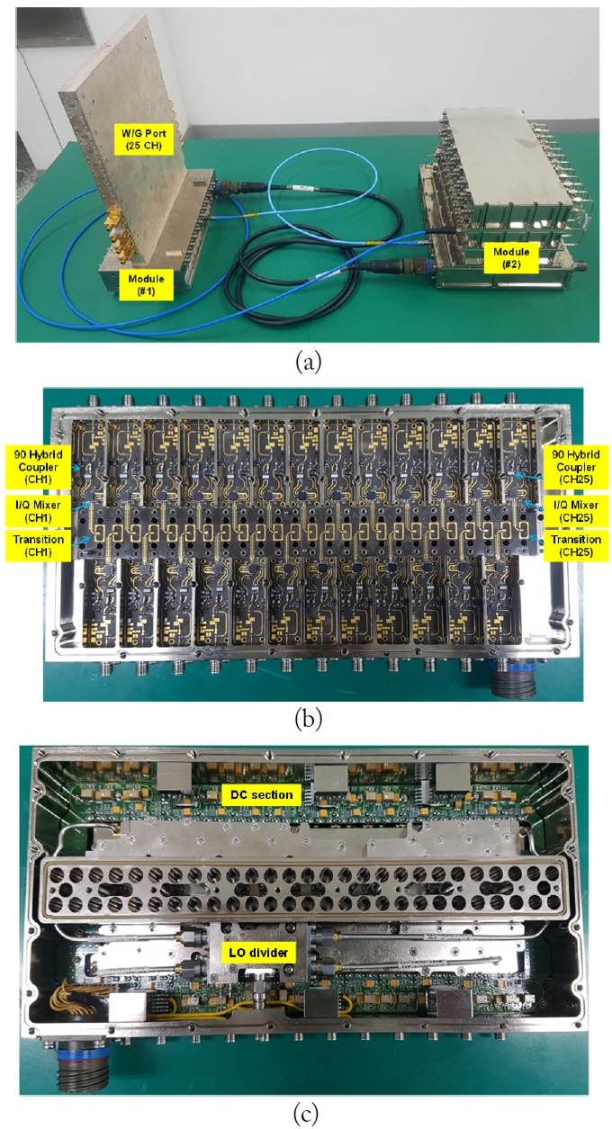
(a) Photograph of the complete setup (from 33–35 GHz to 1 GHz). (b) Photograph of module #1 (RF section). (c) Photograph of module #1 (DC section).
Fig. 9(b) is a photograph of the inside of module #1, which is an area where the RF frequency is mixed with the LO frequency in the mixer (Hittite’s HMC1065LP4E), which includes an image rejection function to output IF signals in the 1 GHz band. The PCB was designed to be installed using the epoxy on the entire bottom surface of the equipment, so that the frequency in the Ka-band could be transmitted through the transmission line without any loss or distortion.
RT/duroid 5880 5-mil PCB was used up to the mixer stage where the Ka band exists, and Rogers RO4003 20-mil PCB was used at low frequencies in the L band converted into IF to make SMT possible.
Fig. 10(a) shows the inside of module #2, Fig. 10(b) the PLL board that generates the LO signal needed to convert the RF frequency into the IF frequency, Fig. 10(c) the IF board for amplifying and filtering the IF signal, and Fig. 10(d) the distribution board in which 25 paths are distributed and switched to 16 paths.
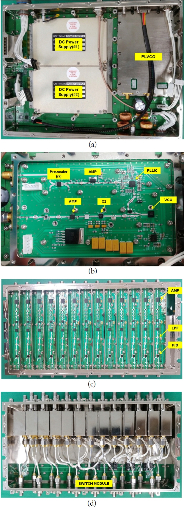
(a) Photograph of module #2. (b) The PLL board including the PLLIC and VCO. (c) The IF board including the AMP and filter. (d) The switch module including the distribution board.
1. GAIN Measurement Results
Fig. 11(a)–(d) show the total gain of channel 1 from the RF input port to the IF output port. As the bandwidth of the IF frequency was about 500 MHz, the total gain was measured four times after changing the RF and LO frequencies to 500 MHz.
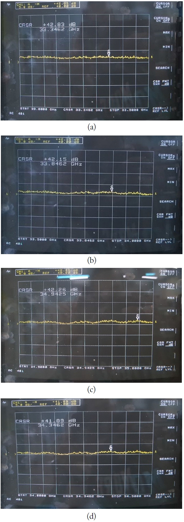
Results of the measurement of gain using a Scalar Net Work Analyzer: (a) 33.0–33.5 GHz band, (b) 33.5–34.0 GHz band, (c) 34.0–34.5 GHz band, and (d) 34.5–35.0 GHz band.
The total gains were as follows:
Up to 42.83 dB in the 33.0–33.5 GHz band
Up to 42.15 dB in the 33.5–34.0 GHz band
Up to 41.89 dB in the 34.0–34.5 GHz band
Up to 42.26 dB in the 34.5–35.0 GHz band
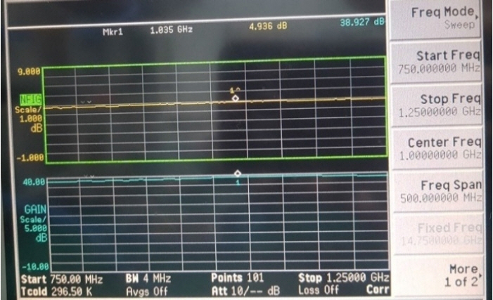
2. NF Measurement Results
As for the results of the measurement of noise figures at the IF frequency in the L band that was changed from the Ka band, which is a receiving frequency band, the value measured at the 0.75–1.25 GHz band was 4.936 dB with a maximum value. This result is mainly due to the noise figure characteristics from the W/G transition structure to the mixer in which the LNA is included. Therefore, the characteristics vary greatly depending on how much the insertion loss is minimized, as shown in Fig. 12.
Results of the measurement of noise figure (IF band).
3. Third Intermodulation Measurement Results
In channel #1, which is representative, the third-order IMD characteristics that show the linearity of the module measured at the center frequency of 1 GHz of the IF frequency was measured as 61.83 dBc (Fig. 13).

Results of the measurement of IM3 (IF band).
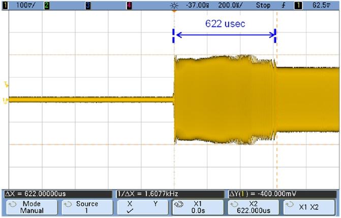
4. Switching Speed Measurement Results
Switching speed is important at the system level because the speed of the switch used to select the RF path determines how fast the signal can be received. It took 622 μs to switch to another channel and select the channel through which the signals came in Fig. 14.
Results of the measurement of the switching speed.
V. Conclusion
In this paper, we designed and fabricated a Ka-band downconverter module with a 25-channel RF input port with a low noise figure, flat gain characteristics, and reliability by applying the chip-and-wire process for assembly into the RF path and operation of a bare-type MMIC device. To compensate for the mismatch among the many components used in the module, W/G transition, an image rejection mixer, a switch, and an amplifier suitable for millimeter-wave frequency characteristics were designed and applied to the downconverter.
The main RF line was a dielectric substrate (RT/duroid 5880), which had a relative dielectric constant of 2.2 and a dielectric thickness of 0.127 mm, and AI203 (ceramic, ATC Co.), which had a relative dielectric constant of 9.8 and a dielectric thickness of 0.254 mm. In the Ka-band downconverter module, the gain was 41.89–42.83 dB at 33.0–35 GHz, with flatness of about 0.94 dB. The measured value of the noise figure at CH1 was 4.936 dB, with a maximum value in the 0.75–1.25 GHz IF frequency. The third intermodulation measurement result was 61.83 dBc. The switch to selecting a channel took 622 μs.
The millimeter-wave (Ka band, 33–35 GHz) 25CH downconverter module proposed in this paper is considered applicable to the modules that are installed at the rear end of the antenna of the SIGINT system in the field of EW to collect signals precisely. However, further studies on how to satisfy and increase the dynamic range still have to be conducted.
Acknowledgments
This work was funded by the technology development business fund of the Ministry of SMEs and Startups in 2019.
References
Biography
Yuseok Jeon obtained his B.S. in electronic communication engineering from Chungju University, Chungju, Korea, in 2000, his M.S. in electronic engineering from Chungbuk National University, Cheongju, Korea, in 2004, and his Ph.D. in electronic and electric engineering at Dankook University, Yongin, Korea, in 2018. He worked as director in R&D division at Broadern Inc., Hwaseong, Korea, from 1999 to 2019. His research interests include the development of transceivers, receivers, and synthesizers using chip-and-wire processes for EW and radar system applications. He received the Korean Engineer Award in 2018.

Jaejin Koo obtained his B.S. in electronic engineering from Soonchunhyang University, Asan, Korea, in 2006 and his M.S. from the Department of Electrical and Communication Engineering, Soonchunhyang University, Asan, Korea, in 2008. He worked as general manager in R&D division at Broadern Inc., Hwaseong, Korea, from 2008 to 2019. His research interests include the development of transceivers and receivers using chip-and-wire processes for EW and radar system applications.

Hyunkyu Kim obtained his B.S. in electronic engineering from Sunmoon University, Asan, Korea, in 2009 and his M.S. in electronic and electric engineering, Dankook University, Yongin, Korea, in 2012. He worked as general manager in R&D division at Broadern Inc., Hwaseong, Korea, from 2009 to 2019. His research interests include the development of transceivers, receivers, RF amp, and GaN transistors using chip-and-wire processes for EW and radar system applications.