Characterization of a 1 mm (DC to 110 GHz) Calibration Kit for VNA
Article information
Abstract
This paper presents an evaluation method for a 1 mm coaxial calibration kit that can be used from DC to 110 GHz. The analytical model for the calibration kit was revisited and verified by comparing it with the electromagnetic High-Frequency Structure Simulator (HFSS). We also proposed a method to measure or appropriately estimate the physical parameters of the analytic model. This approach calculates the uncertainty based on the physical parameters, so that the uncertainty can be appropriately propagated to different measured quantities based on the covariance between all frequencies, including the real and imaginary parts. To verify the proposed method, a commercially available 1 mm calibration kit was evaluated, and the impedance of a device under test was measured using the evaluated kit. We compared the measured results with those of the National Institute of Standards and Technology (NIST) and confirmed that they agreed well with each other within the uncertainty. Additionally, the multiple reflections caused by the impedance mismatch between the signal source and the instrument was corrected, and its calibrated uncertainty was obtained in the time domain. Thus, the uncertainty of the impedance measurement in the frequency domain was properly propagated to the time domain.
I. Introduction
The data transmission rate has been rapidly increasing because of the surge in the use of multimedia and data not only for personal computers but also for other devices such as cellphones. These digital signals should be recognized as the transmission of radio frequency signals because their data rate has a bandwidth of several tens of GHz. As a result, the precise signal integrity measurement is crucial. For example, the impedance mismatch at the discontinuity points on the transmission line can distort the eye diagram significantly. Thus, the impedance mismatch needs to be carefully measured and removed. Moreover, these measurement uncertainties in the frequency domain should be properly propagated to other measurement quantities [1, 2].
In [3, 4], the full covariance matrix for the uncertainty of the impedance measurement was obtained from the physical parameters of airlines. Then, the authors successfully propagated it to the time domain measurement. In [5, 6], the covariance matrix was more easily obtained from the physical parameters of the coaxial (N-type, 3.5 mm and 2.4 mm) SOLT calibration kit. In [2], the authors demonstrated that the covariance matrix could be obtained up to 110 GHz using a commercial 1 mm SOLT calibration kit [7]. The rational fitting model was introduced to evaluate the OPEN and LOAD calibration kit, but its detailed description was not reported.
In this paper, we propose a novel method that obtains an accurate impedance measurement and a covariance matrix up to 110 GHz. To obtain high accuracy, the calibration frequency is divided into two bands based on 50 GHz. In a high-frequency band, multiple offset shorts with different offset lengths are employed because of the simplicity of their structure, which achieves high accuracy. In a low-frequency band, the OPEN and LOAD calibration standards are used to improve the measurement accuracy. These additional references are evaluated using the reciprocal characteristics of a passive device. To validate the proposed method, the measurement result for the impedance is compared with the result of the National Institute of Standards and Technology (NIST). The validation also shows that the obtained covariance matrix through the impedance measurement properly propagates to other measurement quantities.
This paper is organized as follows. Section II describes how to model and evaluate the offset short calibration standards. Section III describes the modeling and evaluation methods of the OPEN and LOAD calibration standards used in the low-frequency measurement. Section IV reviews the measurement results, and Section V concludes.
II. Modeling of the Offset Short
1. Analytic Model
The offset short calibration standards can be modeled analytically because of their simple structure. Fig. 1 shows the cross-section of the offset short consisting of a connector section, a coaxial line, and a shorting plate. Usually, when connecting a coaxial calibration kit, the outer conductors are designed in such a way that their cross-sections meet each other, and the inner conductors are spaced apart from each other to protect them from damage. Therefore, the connector part can be represented with a certain gap, the size of which is generally called the pin depth. The coaxial line represents the offset length, and the shorting plate reflects the incident transverse electromagnetic (TEM) wave. Therefore, the total S-parameter of the offset short can be represented by cascading the three blocks of Sconnector, Sline, and Sreflect.
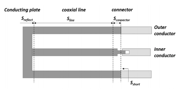
Cross-section of the offset short calibration standard.
The electromagnetic waves incident on the shorting plate can be regarded as being perpendicularly incident on a conductor having a finite conductivity in free space [8]. Therefore, the intrinsic impedance of the conductor, ηsurf, is calculated in Eq. (1) as follows:
where ω, μ, and σ are the angular frequency, permeability, and conductivity, respectively. The scattering coefficient Sreflect of the shorting plate is calculated by (2) with the free space impedance η0.
Fig. 2 compares the S-parameter of the shorting plate calculated using (2) and the simulation result of the High-Frequency Structure Simulator (HFSS version 18.2.0; Ansys Inc., Canonsburg, PA, USA). In the simulation, the shorting plate is modeled with the addition of the coaxial line, and the offset length is de-embedded on the S-parameter. All parts except the shorting plate are set to a perfect electric conductor. The calculation result using (2) agrees well with the simulation of the HFSS.

The low-loss coaxial line filled with air (without dielectric materials) can be assumed not to have conductance G. Therefore, the characteristic impedance Zline and the propagation constant γ can be expressed by Eqs. (3) and (4), respectively.
The inductance L and capacitance C of the transmission line are determined according to the inner diameter d and the outer diameter D as follows:
The lossy conductors also produce the internal resistance Ri and the internal inductance Li as it arises from a flux linkage internal to the conductor surfaces [9].
Therefore, the S-parameter of the coaxial line with length l is as follows [10]:
Fig. 3 shows the comparison results between the derived Eqs. (8) and (9) and the simulation result of the HFSS. The analytic model matches the numerical result of the HFSS in the entire frequency range.

The perturbed impedance by the pin depth of the connector is calculated as follows [11]:
where g is the pin depth, dp is the pin diameter of the connector, and N and w are the number and width of the slot on the female connector (finger socket), respectively. Assume that Zo, Z, and Zo are connected in a series as the gap with impedance Z is placed on the transmission line. Therefore, the S-parameter perturbed by the impedance Z is as follows [9]:
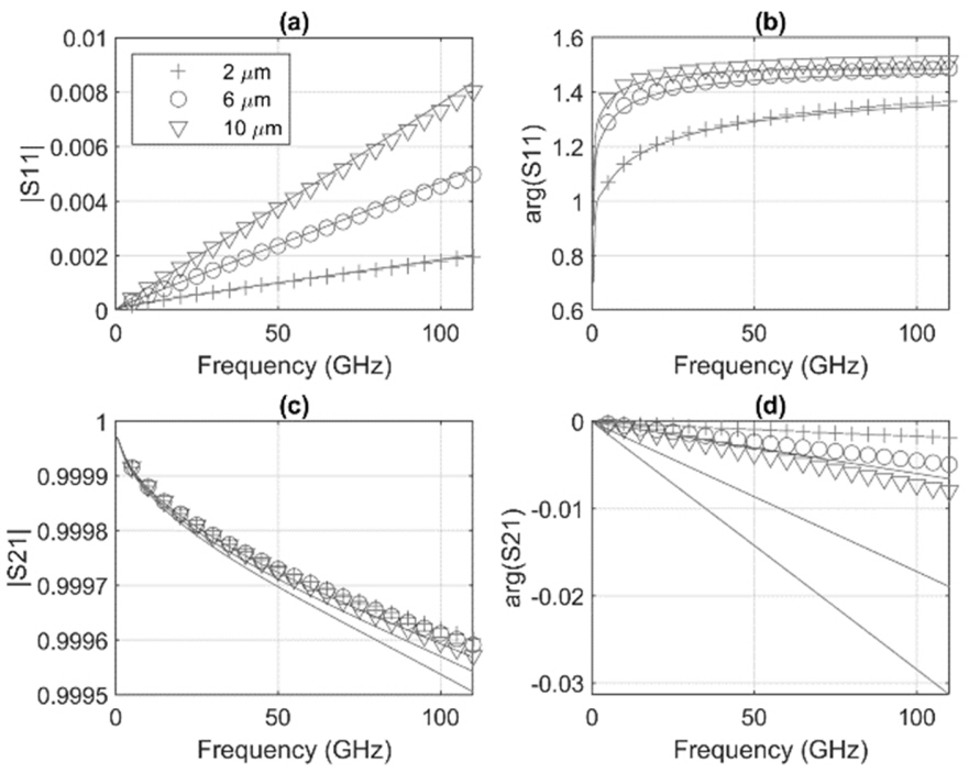
Fig. 4 shows the scattering coefficient of the connector calculated using (11). The result reveals that the predicted S11 is the same as the HFSS depending on the gap size, and a slight difference in S21 is small enough to ignore.
Subsequently, we evaluate the physical parameters used in the analytic model. The offset length and pin depth are verified by measuring whether they satisfy the manufacturer’s specifications. The other physical parameters are found in [12]. The values that are difficult to accurately assess are conservatively set to have large uncertainties. The evaluated parameters with uncertainty are summarized in Table 1.
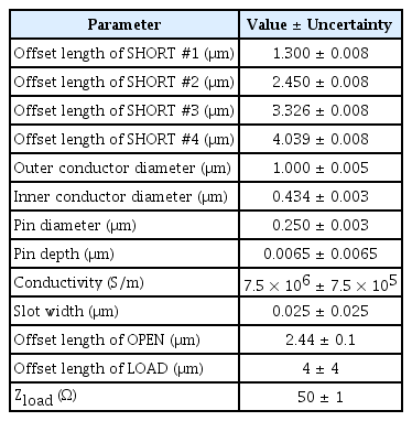
Physical parameters of the evaluated 1 mm coaxial calibration kit
2. Frequency Limit of Offset Shorts
The calibration frequency on the impedance measurement using only offset shorts is limited. Fig. 5 shows the measurement of the OPEN calibration standard using the above four offset shorts. In the measurement, the S-parameters of the offset short vary in the range of uncertainty as summarized in Table 1. The deviation of the measurement is small above 50 GHz and greatly increases below 50 GHz. The reason is that the offset shorts used at frequencies above 50 GHz are sufficiently spaced from each other on the Smith chart through which arbitrary impedances can be accurately measured. However, they converge at a single point below 50 GHz, and the impedances are difficult to precisely measure except around a reflection coefficient of −1. This problem can be solved using additional OPEN and LOAD references that are far from the reflection coefficient −1 below 50 GHz. The following sections describe how to evaluate the OPEN and LOAD calibration standards.
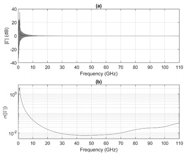
Measurement of the OPEN calibration standard using only multiple offset shorts: (a) reflection coefficient on a dB scale and (b) standard deviation of the reflection coefficient.
III. Modeling of the Open and Load Calibration Standards
Fig. 6(a) and (c) show the physical structure of the OPEN and LOAD calibration standards, respectively. In the case of the OPEN, the insulator with a dielectric constant approximately equal to 1 supports the coaxial inner conductor and creates an electrically open condition. Therefore, it can be regarded as an open termination in the low frequency band as shown in Fig. 6(b). In the case of the LOAD, the end of the coaxial line is terminated with a resistive element to make it reflectionless. As a result, it can be presented as a structure terminated by the impedance Zload as shown in Fig. 6(d).

Modeling of the OPEN and LOAD calibration standards: (a) physical structure of OPEN, (b) equivalent model of OPEN, (c) physical structure of LOAD, and (d) equivalent model of LOAD.
The unknown physical parameters, the offset length L, and the terminated impedance Zload of the OPEN and LOAD are estimated using the reciprocal characteristic of the passive devices. In this case, the 6 dB attenuator is measured with a SOLT calibration method using the offset SHORT#2, the OPEN, and the LOAD. In the calibration process, the unknown physical parameters of the OPEN and LOAD are optimized to minimize the difference between S21 and S12 of the attenuator as shown in Fig. 7. The difference between S21 and S12 is significant before the optimization process, but it is greatly reduced during the optimization process. The determined parameters are shown in Table 1. Their uncertainty is conservatively set to be sufficiently large because it is estimated through optimization and not by measurement.
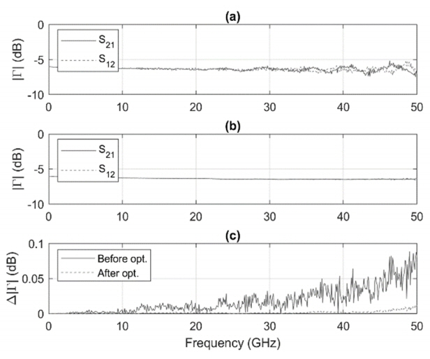
Optimization results of the physical parameters of OPEN and LOAD: (a) before optimization, (b) after optimization, and (c) difference between S21 and S12 of DUT.
IV. Measurements
1. Reflection Coefficient
To verify the characterization method of the calibration kit, we measure the S11 of the DUT and compare it with the result from the NIST. The employed DUT is a photodiode model XPDV412xR produced by Finisar Corp. that consistently produces a wideband pulse up to 110 GHz. The OPEN, LOAD, and SHORT#2 calibration standards are used below 50 GHz, and the offset shorts are only used above 50 GHz with the SOLT calibration method. The 95% confidence intervals for the magnitude of S11 are represented with error bars in Fig. 8(a). The measurement agrees well with the result of the NIST (solid line) at all frequency ranges. The phase of S11 normalized by the result of the NIST is illustrated in Fig. 8(b) with 95% confidence intervals (the current study, dashed line; NIST, solid line). It also confirms that the two results match each other well over the entire frequency range. The large uncertainties around 2 GHz and 28 GHz are due to the small reflection coefficients that make it difficult to obtain accurate phase measurements.
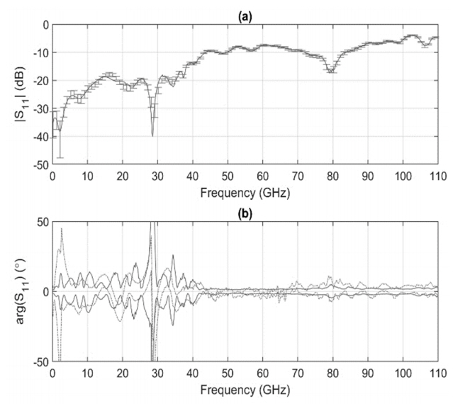
Measurement result of the S11 of DUT: (a) magnitude (the present study, error bar; NIST, solid line) and (b) phase (the present study, dashed line; NIST, solid line).
2. Uncertainty Transformation
The wideband signal is then measured in the time domain. The impedance mismatch between the instrument and the signal source is corrected using (12) by measuring the input impedance Γl of the instrument and Γg of the signal source.
where Vmeas is the Fourier transform of the measured signal. Fig. 9 shows the result of the inverse Fourier transform of the corrected Vcal back to the time domain. Multiple reflections occur between 1.3 ns and 1.5 ns before the calibration (dashed line), but most of these reflections disappear in the corrected result (solid line). The uncertainty can be evaluated using the Jacobian matrix based on (12) and the covariance matrix of the impedance measurement, which is similar to that in [1]. If the uncertainty is evaluated without considering the correlation between frequencies, it will have almost constant values over the entire time interval (see dotted line). Conversely, by calculating the uncertainty from the full covariance based on the physical parameters, it varies with time. In particular, the uncertainty increases in the time interval at which multiple reflections are removed, intuitively indicating that the uncertainty calculation is reasonable.
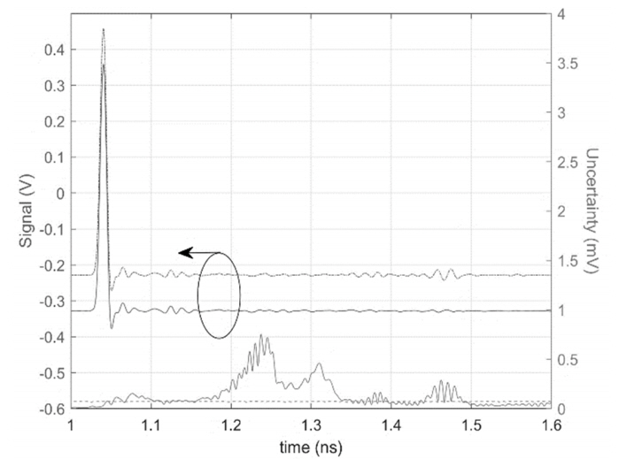
Calibration result and uncertainty in the time domain for the impedance mismatch between DUT and the measurement instrument. For easy comparison, the before the calibration result (dashed line) has an offset of +0.1 V.
V. Conclusions
In this paper, we propose a characterization method of a 1 mm coaxial calibration standard based on the physical parameters. The proposed method obtains the full covariance between the real and imaginary numbers of a complex impedance at all frequencies. As a result, the measurement uncertainty of the impedance can easily propagate to the uncertainty of other measurements. To verify the proposed method, we compare the measured results with the results of the NIST, and they show a good agreement with each other. In addition, our study confirms that the impedance mismatch is effectively removed in the waveform measurement and that the calibration uncertainty propagates well from the frequency domain to the time domain.
Acknowledgments
This research was supported by Physical Metrology for National Strategic Needs funded by the Korea Research Institute of Standards and Science (No. KRISS–2019–GP2019-0005).
References
IEEE Standard for Precision Coaxial Connectors (DC to 110 GHz), IEEE Standard 287-2007 (Revision of IEEE Standard 287-1968), 2007
Biography

Chihyun Cho received B.S., M.S., and Ph.D. degrees in electronic and electrical engineering from Hongik University, Seoul, Korea, in 2004, 2006, and 2009, respectively. From 2009 to 2012, he participated in the development of military communication systems at the Communication R&D Center, Samsung Thales, Seongnam, Korea. Since 2012, he has been with the Korea Research Institute of Standards and Science (KRISS), Daejeon, Korea. In 2014, he was a guest researcher at the National Institute of Standards and Technology in Boulder, CO, USA. He also served on the Presidential Advisory Council on Science and Technology in Seoul, South Korea, in 2016–2017. His current research interests include microwave metrology, time–domain measurement, and standard of communication parameters.

Jin-Seob Kang received B.S. degree in electronic engineering from Hanyang University, Seoul, Korea, in 1987 and M.S. and Ph.D. degrees in electrical engineering from the Korea Advanced Institute of Science and Technology, Daejeon, Korea, in 1989 and 1994, respectively. In 1995, he was a visiting postdoctoral research associate at the Department of Electrical and Computer Engineering, University of Illinois at Urbana-Champaign, Urbana. From 1996 to 1997, he was an assistant professor at the School of Electrical and Electronics Engineering, Chungbuk National University, Cheongju, Korea. In 1998, he joined the Korea Research Institute of Standards and Science (KRISS), Daejeon. His research interests include electromagnetic measurement standards, impedance and antenna measurements, and electromagnetic wave scattering.

Joo-Gwang Lee was born in South Korea in 1960. He received B.S. degree in electronic engineering from Hanyang University, Seoul, Korea, in 1984, and M.S. and Ph.D. degrees from the Korea Advanced Institute of Science and Technology, Daejeon, Korea, in 1994 and 2000, respectively. Since 1986, he has been with the Korea Research Institute of Standards and Science (KRISS), Daejeon. His current research interests include radio frequency and microwave measurements, time–domain metrology, and electromagnetic compatibility.

Hyunji Koo received B.S. and Ph.D. degrees in electrical engineering from the Korea Advanced Institute of Science and Technology (KAIST), Daejeon, Korea in 2008 and 2015, respectively. From March to August 2015, she was a postdoctoral research fellow at the school of electrical engineering in KAIST. Since September 2015, she has been a senior research scientist at the Center for Electromagnetic Standards in the Korea Research Institute of Standards and Science (KRISS), Daejeon, Korea. In 2018, she was a visiting researcher at the National Physical Laboratory, Teddington, United Kingdom. Her current research interests include characterization of on-wafer or PCB devices.