I. Introduction
In recent years, many efforts have been dedicated to improving the operation of ultra-wideband (UWB) microstrip antennas with regard to rapid advances in wireless communication [1, 2]. The main requirements of a UWB microstrip antenna include impedance matching at a frequency bandwidth between 3.1ŌĆō10.6 GHz and a stable gain entirely the frequency bandwidth [3]. To meet these requirements, several techniques have been suggested, such as utilizing defected microstrip structure (DMS), a dielectric substrate with high permittivity, defected ground structure (DGS) at the ground plane, metamaterial (MTM) loading, or a mixture of all these [4ŌĆō6]. Antenna designs with highly desirable features, such as compact size, high performance, low cost, and wide bandwidth, have become ever-growing demands [7, 8]; however, while many frequency-independent antenna designs provide these features, the current paper proposes that a printed, low profile array antenna design may be due to its ease of fabrication and robust overall structure.
Artificial electromagnetic MTMs have properties that are not usually encountered in nature [7]. Thus, there has been much interest in using artificial electromagnetic MTMs in the design of microstrip antennas over recent years [9ŌĆō12]. Approaches to creating an MTM exist within two main categories: resonant and non-resonant [13]. Resonant approaches create an MTM by inducing magnetic and electric dipole moments to achieve negative permeability and permittivity, respectively. However, MTMs designed using this approach have narrow operating bandwidths due to the inherently high-quality factor of their resonant structures [3]. This paper presents a UWB MTM microstrip array antenna that consists of MTM radiation unit cells printed in a planar configuration. Additionally, the behavior of the MTM unit cells is based on the utilization of a resonant approach.
Fractal geometry was introduced by B. B. Mandelbrot at 1975 and was later further investigated by many researchers within the field of antenna design [14]. Koch, Sierpinski, and Minkowski shapes are the most well-known fractal structures that are most often used as wideband and multiband antenna designs due to their self-similarity feature. Another desirable fractal structure used in antenna design is a variety of fractal trees [15, 16]. In this study, a fractal MTM tree microstrip array antenna was investigated. By exchanging the geometry and number of branches of the fractal tree array structures, the antenna specifications could be investigated [14, 17].
Leonard Fibonacci discovered a number sequence while considering a practical problem in the ŌĆ£Liber AbaciŌĆØ involving the growth of a hypothetical population of rabbits based on idealized assumptions [14, 18]. He noted that, after each monthly generation, the number of pairs of rabbits increased from 1 to 2 to 3 to 5 to 8 to 13, etc. and then identified how the sequence progressed by sum the two preceding terms (in mathematical terms, Fn = FnŌłÆ1 + FnŌłÆ2), a sequence which could, in theory, extend indefinitely. This is called the Fibonacci sequence: 0, 1, 1, 2, 3, 5, 8, 13, etc. The Fibonacci sequence appears throughout nature, such as the spiral arrangements of plant leaves, the petals of several flowers, pineapples, artichokes, pine cones, and mature sunflowers [14, 18]. The branch geometry of the proposed MTM microstrip array antenna was designed according to the Fibonacci number sequence and extends from the top of the antenna to its base. Fig. 1 shows some examples of Fibonacci and fractal geometries found in nature.
This paper presents a new family of UWB MTM microstrip array antennas that are based on both fractal and Fibonacci geometric patterns. Specifically, the radiating elements of the antenna were made from left-handed (LH) MTM unit cells placed along one axis, in which each unit cell combines an improved split-ring resonator (SRR) structure with capacitive loaded strips (CLS).
II. Metamaterial Unit Cell
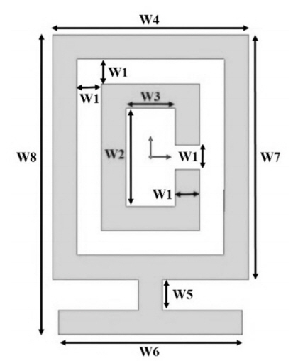
In this study, the prime MTM unit cell was based on SRR structure that includes a smaller loop within a bigger one, with slots incorporated onto each loop at each end. The SRR is a magnetically resonant structure that responds to a perpendicular magnetic field and can be used to obtain negative permeability. The resonant frequency of the SRR structure can be controlled by the slots added to the ring. The primary unit cell is the improved rectangular SRR. This improvement consists of the closing of the loop on the outer ring, which decreases the series capacitance of the SRR. Also, closing the outer ring increases the coupling between the outer and inner ring, which provides a wide backward-wave passband. CLS added to the improved SRR unit cell can then bring the resonance frequency to within the UWB frequency range. The dimensions of the final MTM unit cell are as follows: W1 = 0.4 mm, W2 = 1.6 mm, W3 = 0.8 mm, W4 = 3.2 mm, W5 = 0.5 mm, W6 = 3 mm, W7 = 4 mm, and W8 = 5 mm [3] (Fig. 2).
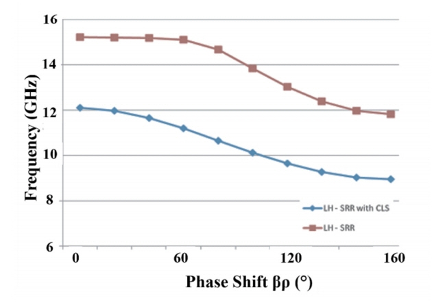
The dispersion diagram shows a plot of the phase velocity (╬▓) versus the eigenfrequency of the structure (f) used to specify the MTM unit cell resonance frequency and determine the areas in which the structure exhibits either right-handed (RH) or LH specifications by a positive or negative slope, respectively. As shown in Fig. 3, the dispersion diagrams of the improved SRR/CLS and SRR structure are plotted in blue and red, respectively. It can be observed that the resonance frequency of the LH mode of the SRR/CLS structure is now within the UWB frequency range [3].
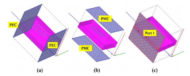
All materials can be characterized electrically by their complex permeability (╬╝) and permittivity (╔ø) in the frequency domain. These fundamental parameters specify the response of a material to electromagnetic radiation. In order to calculate the plots for the complex permeability and permittivity of the MTM unit cell, a retrieval method utilizing the S-parameters was employed. The S-parameters of the MTM unit cell were extracted via a HFSS simulator, which is a finite-element-method (FEM)-based full-wave simulation [1, 19]. According to the periodic repetition of the MTM unit cell, the composition of the perfect magnetic conductor (PMC) and perfect electric conductor (PEC) boundary conditions simulated the periodic boundary conditions using the symmetry inherited by the MTM, as shown in Fig. 4(a) and (b). When the periodic boundary conditions were determined, the excitation ports simulated the incident wave that propagated from the top to the bottom of the unit element, as shown in Fig. 4(c). The S-parameter plots of the MTM unit cell extracted by HFSS are shown in Fig. 5.
Permeability (╬╝) and permittivity (╔ø) are related to the impedance and refractive index through the following expressions [19]:
where z is the impedance, n is the refractive index, d is the maximum length of the unit element, k0 is the wave-number, and m is the branch due to the periodicity of the sinusoidal function.
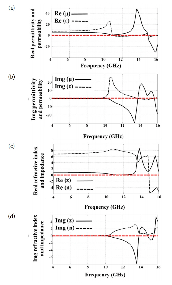
After the S-parameter results were extracted by HFSS, using a MATLAB script, which used the presented mathematical formulation, the complex permeability and permittivity plots were obtained [1, 18] (Fig. 6(a) and (b)). Also, the impedance and refractive index are shown in Fig. 6(c) and 6(d). As shown in Fig. 6, the MTM unit cell had a negative refractive index at approximately the resonance frequency.
III. The UWB MTM Microstrip Array Antenna
MTM unit cells, due to the surface current that forms upon them, are radiating sources. This surface current is related to the electric and magnetic dipole moments of the CLS and SRR, respectively. When the MTM unit cell is excited by its eigencurrents, it can be an efficient source of radiation. So, the capability to excite the eigenfrequencies of a MTM unit cell will enable its application as an effective radiating source.
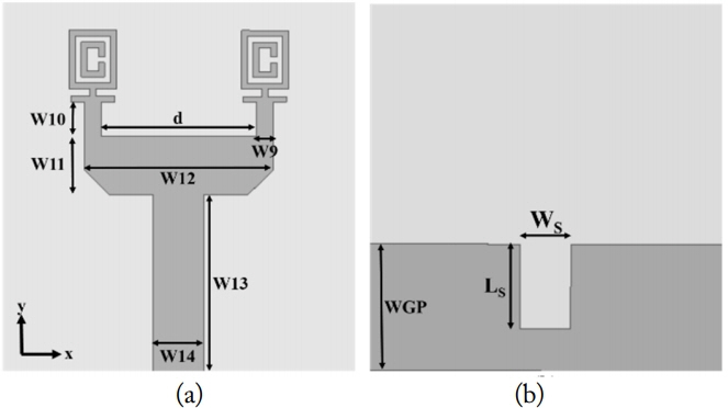
Thus, the MTM unit cell was used to create a two-element microstrip array antenna, in which the two MTM unit cells were positioned in the x-direction, as shown in Fig. 7(a). In order to promote an even field distribution and the excitation of the MTM unit cells, a dual-shaped feed was used in the antenna structure. The top layer footprint of the antenna is 21 mm ├Ś 22mm, and the other dimensions of the antenna structure labeled in Fig. 7(a) are as follows: d = 9.2 mm, W9 = 1 mm, W10 = 2 mm, W11 = 3.5 mm, W12 = 11.2 mm, W13 = 10.5 mm, and W14 = 3 mm.
Low energy storage structures have a higher Q factor and thus their bandwidths are wider. Therefore, a partial ground plane with WGP = 7.5 mm was used to improve matching and increase the bandwidth of the antenna. Also, in order to obtain greater improvements, a rectangular slot with length LS = 5 mm and width WS = 3 mm was introduced to the center of the partial ground plane. The optimization of WS and LS helped achieve the wideband matching. The bottom layer of the array antenna structure is shown in Fig. 7(b).
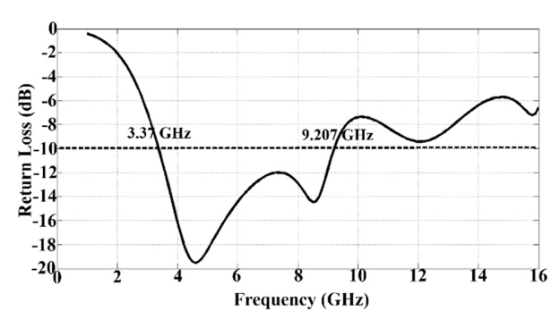
The UWB MTM two-element array antenna structure was analyzed using the HFSS software. The substrate is FR4 with a dielectric constant ╔ør = 4.3, thickness h = 1.6 mm, and a loss tangent tan ╬┤ of about 0.025. As shown in Fig. 8, the ŌłÆ10 dB impedance bandwidth of the UWB MTM array antenna ranged from 3.37 GHz to 9.207 GHz under simulation.
IV. The Proposed UWB MTM Microstrip Array Antenna
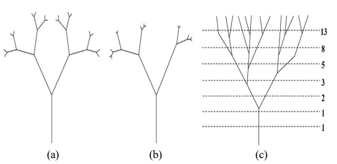
In this study, the theory and design of a new family of UWB MTM microstrip array antennas, based on fractal and Fibonacci geometric patterns, were investigated. It was found there is a relationship between the electromagnetic behavior of an antenna and the properties of fractal geometry. In recent years, many two- and three-dimensional fractal tree antennas, which have similar forms and uniform branch length ratios, have been used in antenna design. Moreover, the number of branches in a fractal tree array antenna increase with respect to the number sequence 1, 2, 4, 8, 16, 32, etc. from the top of the antenna to its bottom, and the branch length ratio is 1/2, as shown in Fig. 9(a).
As shown in Fig. 9(b), whenever the number of branches in creases with respect to the Fibonacci number sequence, the complexity of the fractal tree array antenna decreases. So, the Fibonacci tree array antenna with a same iteration exhibits less complexity due to its reduced number of branches. Determining the number of branches using the Fibonacci sequence leads to non-uniform branch ratios in the tree antenna. As shown in Fig. 9(c), another tree configuration was generated by changing the number of branches based on the modified Fibonacci sequence: 1, 2, 3, 5, 8, 13, etc. This is called the Dream tree, which shows the growth of the rabbit population mentioned in the introduction.
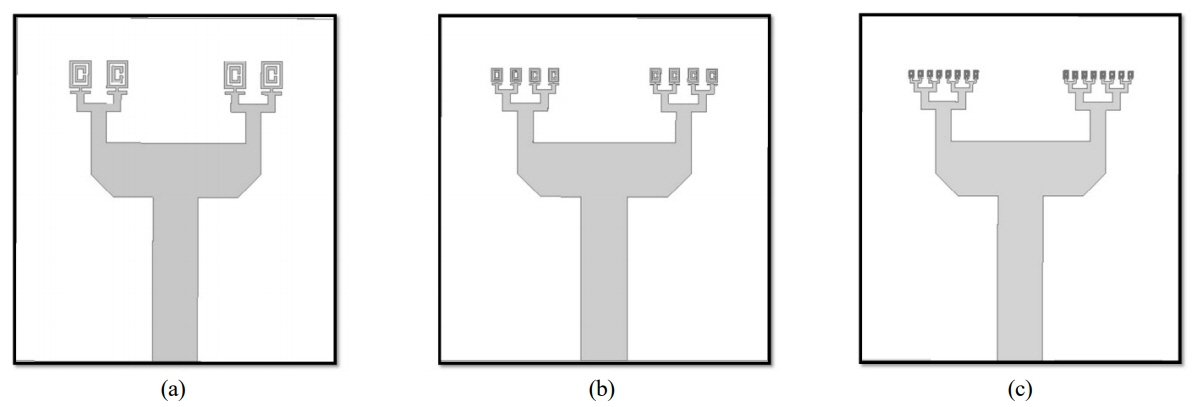
The fractal UWB MTM array antenna was generated by applying an iterative procedure to the MTM two-element array antenna. Upon the first iteration, each MTM element of the two-element array was split into two branches at a 1/2 ratio. The iterative process then continues to generate second- and third-order fractal MTM array antennas. These antennas have closed structures, as shown in Fig. 10. The number of branches increased according to the number sequence 1, 2, 4, 8, 16, 32, etc. from the top of the antenna to its base. Also, their branch area ratios are 1/2, which are also uniform.
The special proposed array antenna, designed using the Fibonacci number sequence is called the Fibonacci UWB MTM microstrip array antenna and is obtained in a similar way as the previous proposed array antenna which was based on fractal geometry. Upon the first iteration of the Fibonacci proposed array, one of the MTM two-element array branches was split into two branches at a 1/2 ratio, through the left or right branch. The other branch was positioned in the same direction as the previous branch ratio, as shown in Fig. 11(a). The iterative process continues on to generate second- and third-iteration Fibonacci MTM array antennas similar to the dream tree, as shown in Fig. 11(b) and (c). The branch numbers increase according to the number sequence 1, 2, 3, 5, 8, 13, etc., from the top of the antenna to its base. Also, the branches of the Fibonacci array have non-uniform area ratios due to non-uniform geometry of the Fibonacci tree.
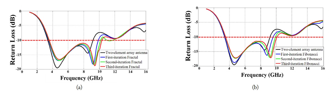
The proposed fractal and Fibonacci structures were analyzed via a HFSS simulator using the same two-element MTM array antenna substrate in order to compare the return loss results. Table 1 shows their simulated return loss and metal areas. It can also be seen that the frequency bandwidth of the proposed third-iteration fractal and Fibonacci structures yields an impedance bandwidth of about 961 MHz and 770 MHz more than the two-element MTM array antenna bandwidth, respectively. The proposed array antennas have a greater number of MTM radiation elements that are closer to each other in comparison with the two-element array antenna. So, mutual coupling between these elements more greatly affect the near fields of the antenna. According to this fact, the input impedance of an antenna is affected by the near and far fields can lead to an improvement of the impedance bandwidth of the proposed array antenna. However, from another point of view, as the iteration order of the proposed array antennas increases, greater metal area reduction results. This metal area reduction decreases the capacitance of the patch array antennas, which, in turn, leads to quality factor reduction in the equal circuit of the proposed antenna and, thus, the impedance bandwidth improves.
Fig. 12 shows a comparison between the return loss simulation results of the two-element and proposed UWB MTM array antennas. Also, the fractal and Fibonacci third-iteration array antennas have lower radar cross-section (RCS) due to 4.95 % and 4.02% metal area reductions, respectively.
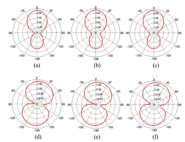
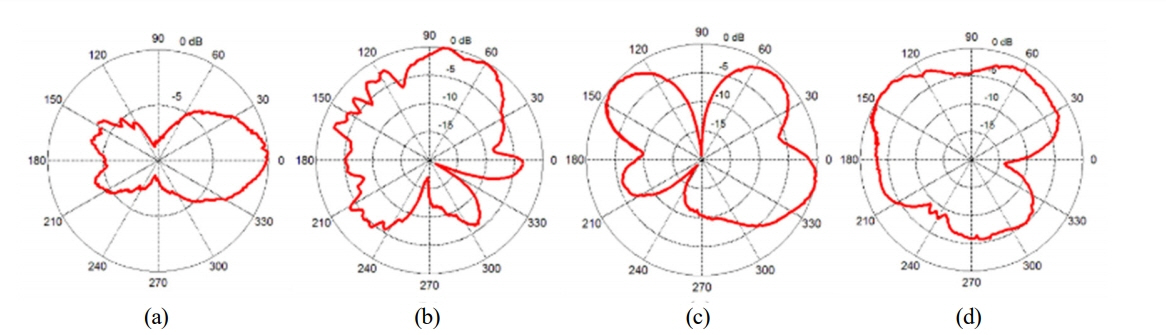
The simulated E-plane and H-plane radiation patterns of the two-element UWB MTM microstrip array antenna (Antenna 1), the proposed first-iteration fractal UWB MTM microstrip array antenna (Antenna 2), and the proposed first-iteration Fibonacci UWB MTM microstrip array antenna (Antenna 3) at 7.3 GHz are shown in Fig. 13. As shown, the radiation patterns of Antennas 2 and 3 are similar to that of Antenna 1. The radiation elements added at a higher iteration are smaller and fed by appropriate amplitude and phase feed. Thus, Antennas 2 and 3 only yield a slight improvement in antenna directivity, while the shape of the radiation pattern does not change. Moreover, the gain of the proposed antennas is slightly improved. Specifically, this increase in proposed array antenna gain is due to the presence of a greater number of MTM radiation elements.
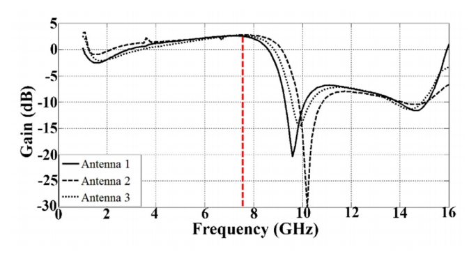
In order to compare the maximum gain of the proposed fractal and Fibonacci structures with the two-element MTM array antenna, the gain versus the frequency curves was extracted via HFSS frequency domain simulation. As shown in Fig. 14, the simulated results indicate that the maximum gain occurs at a frequency near 7.3 GHz for the all the antennas. Specifically, the maximum gains of Antenna 1, 2, and 3 are 2.58, 2.69, and 2.61 dBi, respectively.
The results of a parametric study on the distance between the branches (d = 4ŌĆō13 mm parametric sweep) of Antenna 3 is shown in Fig. 15. In the first choice, d = 7 mm (red line) is the optimum distance due to the maximum frequency bandwidth result, but it can be seen that the simulated return loss of the antenna around 8 GHz is slightly less than ŌłÆ10 dB. So, in this study, d = 10 mm (yellow line) was chosen as the optimum distance due to its wide and safe bandwidth in comparison with all the distances.
V. Measurement Results and Discussion
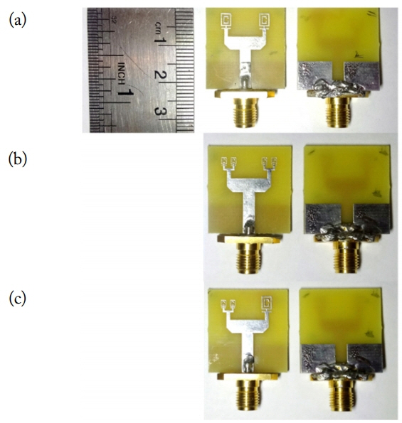
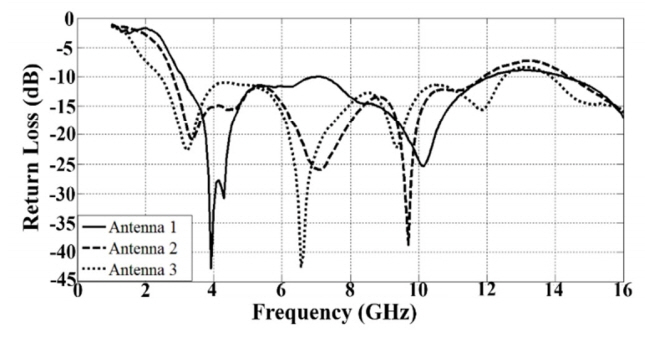
Antennas 1ŌĆō3 were fabricated using the FR4 substrate with a thickness of 1.6 mm and a relative permittivity of ╔ør = 4.6, as shown in Fig. 16. The return loss of all three antennas was measured via network analyzer Agilent 8722ES, as shown in Fig. 17. Fig. 18 shows the measured return loss results of the three antennas at the 1ŌĆō16 GHz frequency band. As shown in Fig. 18, Antennas 2 and 3 have broader frequency bandwidths. Due to the small size of the antennas and their wide bandwidth at high frequencies, manufacturing error, fabrication accuracy, and measuring device calibration all contributed to the difference between the simulation and measured results.
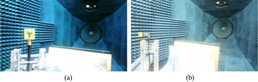
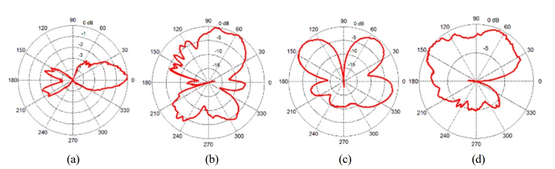
The co-pol and cross-pol radiation patterns of the fabricated antennas ere measured at the E-plane and H-plane at a 7.3 GHz frequency. Fig. 19 shows the measurement of the co-pol and cross-pol radiation patterns in a tapered anechoic chamber of ITRC (Iran Telecommunication Research Center). Figs. 20ŌĆō22 show the measured radiation pattern results of the fabricated antennas. Additionally, the gain of the fabricated antennas was measured in the main lobe direction at four frequencies. Table 2 and Fig. 23 show the measured gain results of the fabricated antennas. It can be seen from Table 2 that the maximum gains of Antennas 2 and 3 improved by 1.24 dBi and 3.14 dBi, respectively, in comparison with Antenna 1 at a 7.3 GHz frequency.
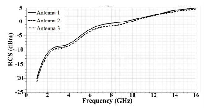
In practice, due to the small size of the antennas, there was no possibility of measuring the RCS in the anechoic chamber; thus, there is no data on the RCS measurements. However, as shown in Fig. 24, the RCS simulation results show that Antenna 2 and Antenna 3 have lower RCS of about 1ŌĆō1.2 dB due to 2.88% and 1.44% metal area reductions, respectively.
VI. Conclusion
A new family of the UWB MTM microstrip array antenna has been proposed. The proposed antenna design consists of MTM unit cells that comprise an improved SRR structure with CLS. The left-handedness of the unit cells was demonstrated via a dispersion diagram and permittivity and permeability curves. Fractal and Fibonacci geometric patterns were used to design a new prototype of MTM array antennas. For comprehensive study, the first iteration of the fractal and proposed Fibonacci antennas were designed, fabricated, and measured. Numerical and experimental results both confirmed that the frequency bandwidth of the proposed antennas increased, while their RCS decreased due to metal area reduction. The proposed antenna also exhibited omni-directional radiation specifications in the H-plane at the frequency bands of interest, a requirement for wireless applications. In all, the proposed antenna is suitable for use in wireless applications due to its low cost, compactness, low profile, low RCS, and wide bandwidth.