I. Introduction
With increasing demands for high data rate services and the miniaturization of portable radio devices, the challenge of supporting multiple air interface technologies that enable compact multi-mode multi-band devices has become critical [1, 2]. Currently, the market for electrically controllable matching circuits, tunable voltage-controlled oscillators (VCOs), tunable filters, and multi-band power amplifier modules (PAM) is growing rapidly [3ŌĆō5]. Digitally tunable capacitors using complementary metal-oxide-semiconductors (CMOS) or microelectromechanical system (MEMS) switches have been widely used to meet these technical trends [6ŌĆō8].
A digitally tunable inductor can be realized by physically changing the metal line length of an inductor with switches. Losses of the switches and metal lines have always been limiting factors in commercializing high-quality (Q) tunable inductors. MEMS-applied tunable inductors have been studied due to their low losses [9, 10]. However, they suffer from several drawbacks, such as complexity, difficulty in monolithic integration with other ICs, and reliability problems [11, 12]. Analog control with MEMS actuators and digital control with MOS switches have been employed to realize the tunable inductors [13ŌĆō15], but these inductors have drawbacks in Q-factor, tuning range, and action voltage.
We propose a high-Q and wide tunable bondwire inductor (TBI) digitally controlled by RF CMOS switches. The bondwire inductors are adopted because their self-resistance and standard manufacturing process cost are much lower than those of spiral inductors [16, 17]. The RF switches are designed using 180 nm silicon-on-insulator (SOI) CMOS technology to minimize their turn-on resistance. The performance of the proposed TBI is compared with other research results.
II. Design of the Tunable Bondwire Inductor
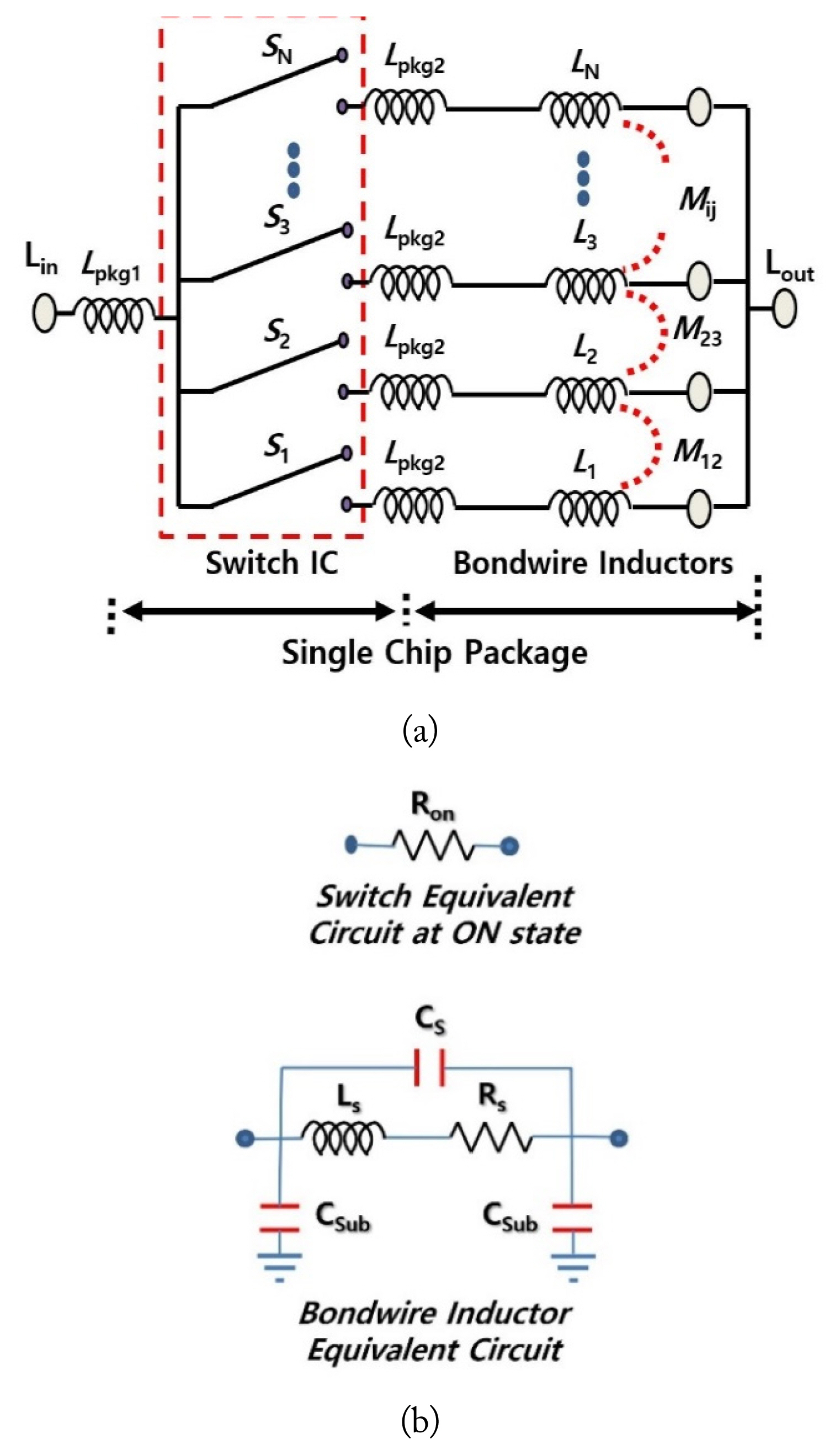
The basic schematic of the proposed TBI and the related equivalent circuits are shown in Fig. 1. The RF switches (S1, S2, ┬Ę┬Ę┬Ę, SN) and inductors (L1, L2, ┬Ę┬Ę┬Ę, LN) are connected in series, which are connected in parallel between nodes Lin and Lout. Lpkg1 and Lpkg2 are the inductance of the bondwire used to package the switch integrated circuit (IC), Mij is the mutual inductance between ith and jth inductors, and Ron is the resistance for the switch ŌĆ£onŌĆØ state [18, 19]. The CMOS switch is made of 12 field-effect transistors (FETs) stacked for a high-power handling capability of up to 35 dBm. It is designed to have low Ron with an enlarged gate width for a high Q characteristic. The bondwire inductor is based on the single ŽĆ-model [20]. When the number of inductors connected in parallel increases, the total inductance decreases, and the role of the low-loss Lpkg1 becomes more important. The overall Q characteristic of the proposed TBI significantly depends on the resistance of the bondwire (Lpkg1 in Fig. 1) used to package the switch IC. To reduce-the resistance, double bonding wire is used. This has been found to significantly enhance the overall Q. Spiral inductors on CMOS substrates usually have low Q-factors because of their high conductor loss, caused by thin metal lines and high dielectric loss. In order to solve these electrical problems, the proposed TBI is designed on a package substrate. The schematic diagram of this proposed TBI is shown in Fig. 2. The positions of the four bondwire inductors achieve a high Q factor by optimizing the configuration of the TBI using an electromagnetic (EM) field simulator that takes into account mutual inductance.
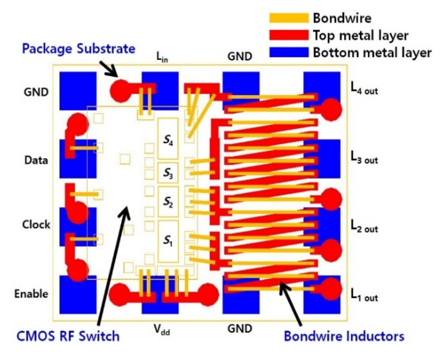
For the wide tuning range and monotonous increase of inductance, the final inductance values for the single-pole four-throw (SP4T) switch IC and four bondwire inductors are Lpkg1 = 0.5 nH, L1 = 4.7 nH, L2 = 6 nH, L3 = 10.5 nH, and L4 = 3.2 nH. These inductance values have been finalized with EM-simulated optimization using a High-Frequency Structure Simulator (HFSS; Ansys Inc., Canonsburg, PA, USA) and starting from a theoretical calculation. The bondwire inductors are implemented on a chip-on-board (COB) substrate with low-loss dielectric material and a thick top metal layer. As such, the loss for the TBI becomes smaller than that for the wafer-level bondwire inductor. Bondwire inductors with low inductance are more sensitive to the internal resistance of the RF switch than those with high inductance. Thus, the switch S4 for the inductor L4 is designed to have the lowest internal Ron among the four used switches. The SP4T switch IC is controlled through a 3-wire (clock, data, and enable) serial peripheral interface (SPI) and is usually powered using Vdd (Fig. 2) of about 3.3 V.
III. Fabrication and Measurement Results
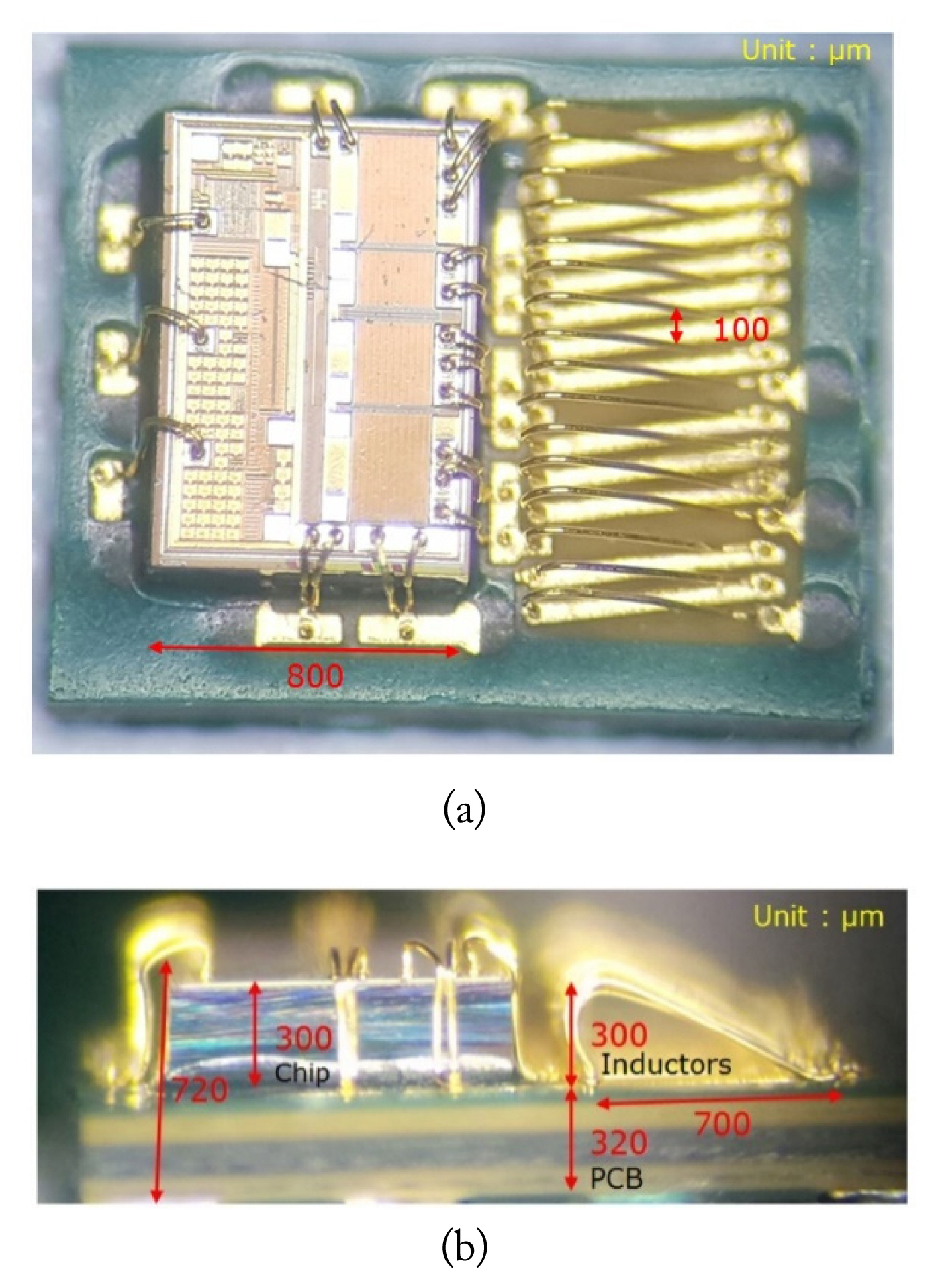
A prototype TBI was fabricated using a COB assembly process to verify the feasibility of the proposed configuration. Photographs of the prototype are shown in Fig. 3. The size of the module consisting of four bondwire inductor arrays and an SP4T RF switch was 2.0 ├Ś 2.4 ├Ś 0.8 mm3. The size of the fabricated SP4T switch with the SPI communication block was 1.3 ├Ś 0.8 ├Ś 0.3 mm3. It used thin-film SOI 180 nm CMOS RF switch technology. During fabrication of the TBI, the switch chip was die-bonded on a package substrate (Fig. 2), and the wire bonding for the bondwire inductor and chip packaging was performed using 1 mil (25.4 ╬╝m) diameter gold wire. The separation between the bondwires is 100 ╬╝m. The height of the bondwires is 300 ╬╝m, and the total length of a single bondwire is 1.06 mm. The fabricated chip was measured using a Keysight E5071C network analyzer (Keysight Technologies Inc., Santa Rosa, CA, USA) with a short-open-load-through (SOLT) calibration and de-embedding.
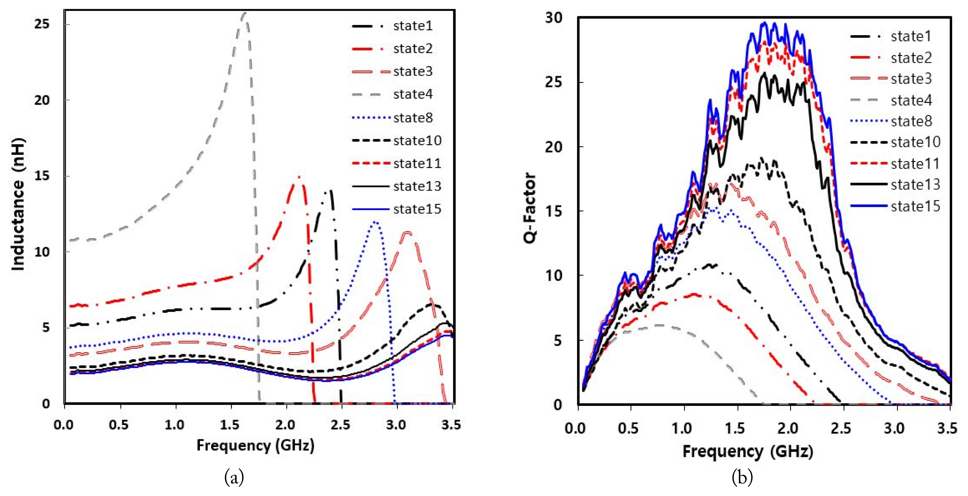
Table 1 lists the performance of the TBI depending on states of 4-bit switch combinations. The fabricated TBI chip exhibits a variable inductance from 1.77 to 11 nH at 0.1 GHz. The maximum Q of 29.5 occurs at 2.1 GHz in state 15, where the self-resonant frequency (SRF) is 4.42 GHz.
The measured inductances and Q-factors are shown in Fig. 4 as a function of frequency from 0 to 3.5 GHz. The measured inductance of the TBI shows a monotonically increasing characteristic. In Fig. 4(b), the states with two or more bondwire inductors are shown to have higher Q characteristics than those with one bondwire inductor. These high Q characteristics are obtained by minimizing the turn-on resistance of the RF switch with an enlarged gate width, minimizing the self-resistance of package bondwire with a double bondwire connection, and optimizing the configuration of the TBI using the 3D EM simulation tool.
The measured inductances and Q-factors for all states at 1.5 GHz and 2 GHz are shown in Fig. 5. A higher Q occurs with more parallel-connected inductors, as in states 11 and 15. When the number of parallel inductors increases, the TBI has an additional magnetic flux due to the mutual coupling. The parallel inductance by the bondwire inductors becomes small so that the effect of the inductance of Lpkg1 used as a package is relatively high. Therefore, a higher Q is achieved with more parallel-connected TBIs.
In Table 2, the performance of the proposed TBIs are compared with others [13ŌĆō15, 20ŌĆō27] in terms of primary inductance, size, tuning range, Q-factor, and action voltage. Due to the narrow tuning range characteristics below 233 and the need for voltage above 7 V or special operating signals, the tunable inductors [14, 15, 20ŌĆō26] using MEMS actuators have limitations for general product applications. In Park et al. [13], a multi-layer stacked inductor switched by MOSFETs is reported. The main drawback of this device is its low Q, caused by parasitic losses of the transistor. In Wainstein and Kvatinsky [27], two topologies, a memristive-via switched tunable inductor and a multi-layer stacked inductor tuned by RF memristive switches, are proposed and simulated using Advanced Design System (ADS). By improving the parasitic losses of the switch, Wainstein and Kvatinsky [27] obtain a higher Q than Park et al. [13]. TBI has the advantages of complete SPI control, wide tuning range by 4-bit control, and high Q using bonding wire inductors. Overall, the proposed TBI is superior to others.
IV. Conclusion
The proposed tunable bondwire inductor has been shown to exhibit a wide (521%) tuning range, from 1.77 to 11 nH at 0.1 GHz. It has also shown high Q-factors, with a maximum of 29.5 when four inductors are all connected in parallel. These competitive results have been obtained using thin-film SOI 180 nm CMOS RF switch technology and wire bond technology.
The proposed tunable inductor is a promising key component for such uses as electrically controllable RF circuits, filters with wide tuning range, and matching circuits for various applications.