I. Introduction
Power dividers are passive components essential for configuring wireless communication and equipment. Recently, many studies have been conducted regarding the application of asymmetric splitters to circuits with various uses, such as Doherty amplifiers [1] and antenna feeders [2]. Conventional asymmetric splitters have employed quarter-wavelength transmission lines of low and high impedances according to splitting ratios. However, the transmission line width of asymmetric splitters is either extremely large or extremely small to be implemented using microstrip technology.
To overcome implementation problems such as that of the planar structure microstrip, a thick material with a low dielectric constant [3ŌĆō5], a suspended strip structure [6], or a defected ground structure (DGS) [7] can be used to realize a high-impedance transmission line. In addition, because low-impedance transmission lines have very large line widths, a structure with open-circuit stubs connected in parallel to the transmission line can be used to implement a suitable low-impedance transmission line [8]. However, the methods that use thick material or mechanical structures for low- or high-impedance transmission lines are applicable under limited conditions only.
In this study, to implement high- or low-impedance transmission lines, we propose an impedance control method for converting a two-port transmission line into a three-port transmission line. This method uses a three-port transmission line with an adjusted scaling factor that increases or decreases the internal impedance of the converted transmission line. In addition, it operates the equivalent circuit as one that connects open- or short-circuit stubs in parallel to each port on the three-port impedance line.
Using this method, an asymmetric power divider was designed by converting its low- and high-impedance transmission lines into suitable uniform impedance transmission lines that were connected in parallel to open- or short-circuit stubs. As an example, a 9:1 asymmetric Wilkinson power divider and a 5:1 Gysel power divider [9ŌĆō11] were designed and measured at an operating frequency of 2 GHz.
II. Theory of Impedance Control Method
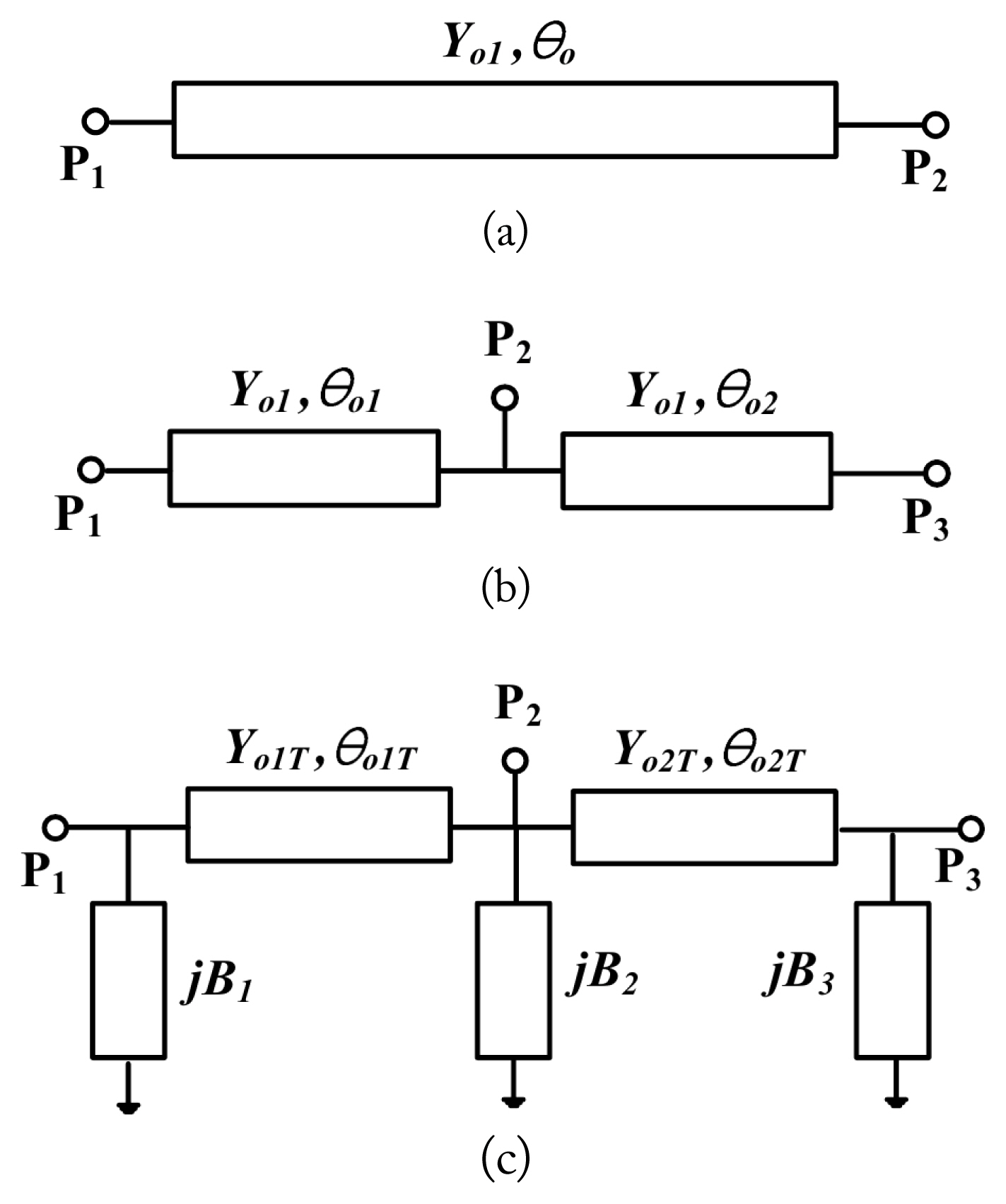
Fig. 1(a) depicts a transmission line with a characteristic admittance Yo1 and electrical length ╬Ėo. This transmission line can be modified with port 2 inserted in the middle, as shown in Fig. 1(b) [12, 13]. The electrical length of the modified transmission line is
In this case, the admittance parameters of the transmission line to which port 2 is added are
(2)
Without affecting the termination impedance of port 1 and 3, the internal impedance of port 2 can be adjusted by multiplying row 2 and column 2 of (2) by a scaling factor ╬▓ that describes the ratio of internal impedance to terminal impedance. The result obtained after multiplying the scaling factor is given by (3).
(3)
The internal impedance converted circuit can be implemented as a transmission line circuit in which stubs are connected in parallel to each port. Its equivalent circuit is illustrated in Fig. 1(c). The admittance parameters of this equivalent circuit can be expressed as
(4)
Because (3) and (4) should be the same as those for equivalent circuits, the following expression can be obtained.
The susceptance Bi (i = 1, 2, 3) can be implemented in open-or short-circuit stubs with admittance values and electrical length indicated in (6).
(7)
the admittances Yo1, Yo1T, and Yo2T will have the following relationship:
This means that if condition (7) is satisfied, the transmission line of the equivalent circuit in Fig. 1(c) can be converted to obtain an impedance value lower than the original one.
In addition, if the conditions satisfy the relation,
(9)
the transmission line of the equivalent circuit can be converted into a line with an impedance value higher than the original one.
To obtain B1, B2, and B3, the conditions of (5b) and (5d) are substituted into (5c), and the result is as follows:
(11)
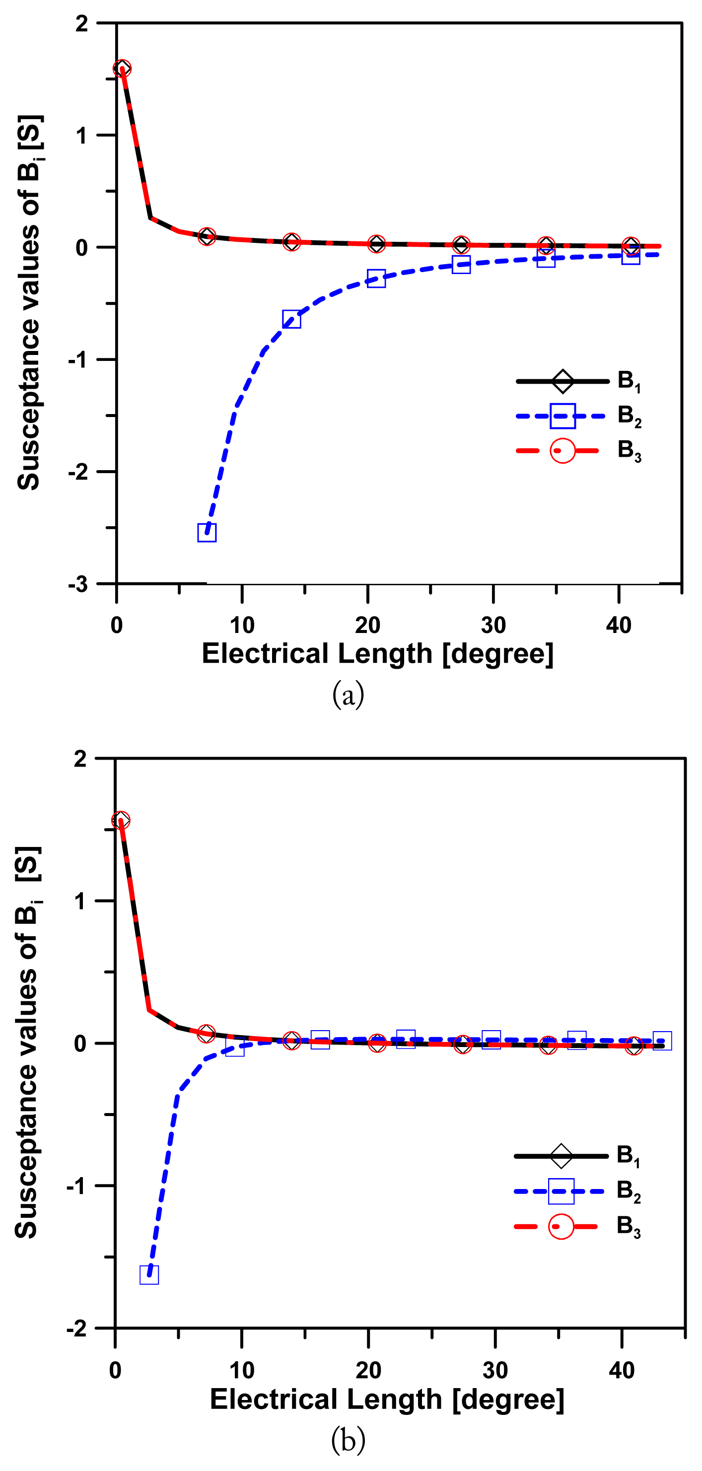
Fig. 2(a) displays the variation of B1, B2, and B3 when ╬Ėo1T and ╬Ėo2T change from 0┬░ŌĆō45┬░ under characteristic admittances Yo1 = 0.003663 S and Yo1T = 0.01254 S, with electrical lengths ╬Ėo1 = ╬Ėo2 = 45┬░. Furthermore, Fig. 2(b) shows the variation of B1, B2, and B3 when ╬Ėo1T and ╬Ėo2T change from 0┬░ŌĆō45┬░ under characteristic admittances Yo1 = 0.03289 S and Yo1T = 0.01254 S, with electrical lengths ╬Ėo1 = ╬Ėo2 = 45┬░.
III. Simulation and Experimental Results
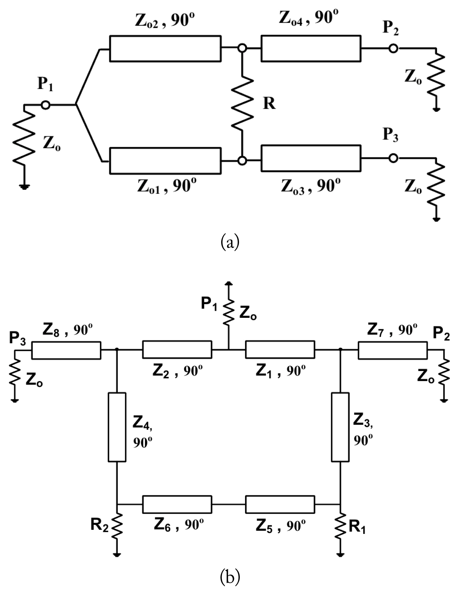
Fig. 3 presents the schematics of a Wilkinson power divider and a Gysel power divider with splitting ratio of 9:1 and 5:1, respectively. The impedance values of each quarter-wavelength transmission line are provided in Tables 1 and 2.
To design high- and low-impedance transmission lines in Tables 1 and 2 using the impedance control method, a Rogers printed circuit board with a dielectric constant of 3.48, a dielectric thickness of 0.762 mm, and a copper thickness of 0.035 mm was used.
The simulation was performed using Microwave Office software version 13 developed by Cadence Design Systems Inc.
In the Wilkinson power divider, first, for the transmission line of 273.8 ╬® with ╬Ėo1 = ╬Ėo2 = 45┬░, a microstrip line width capable of implementing this line was selected as 0.7 mm (characteristic impedance of 79.7 ╬®), and the electrical lengths were determined to be ╬Ėo1T = ╬Ėo2T = 36┬░. The scaling factor of this design condition was ╬▓ = 4.13348, and its susceptance values were calculated as B2 = ŌłÆ0.09024 and B1 = B3 = 0.01362.
Because B2 is negative, the short-circuit stub was implemented at a line width of 0.4 mm (characteristic impedance of 99.8 ╬®) and an electrical length of 6.3┬░ using 0.4 mm via holes. Further, because the B1 and B3 values are positive, the line width of the open-circuit stub was implemented at 3.5 mm (characteristic impedance of 30.5 ╬®) and an electrical length of 22.5┬░.
Second, for the transmission line of 30.4 ╬® with ╬Ėo1 = ╬Ėo2 = 45┬░, a microstrip line width capable of implementing this line was selected as 0.7 mm (characteristic impedance of 79.7 ╬®), while the electrical lengths were determined to be ╬Ėo1T = ╬Ėo2T = 31.5┬░. The scaling factor of this design condition was ╬▓ = 0.51666, and its susceptance values were calculated as B2 = 0.0234 and B1 = B3 = ŌłÆ0.01239.
Using the B2 value, the line width of the implemented open-circuit stub was implemented at 3.5 mm (characteristic impedance of 30.5 ╬®) and an electrical length of 35.5┬░.
In addition, using the B1 and B3 values, the line width of the short-circuit stub was implemented at 0.4 mm (characteristic impedance of 99.8 ╬®) and an electrical length of 38.9┬░ with 0.4 mm via holes.
At the intersection point of Zo1 and Zo2, the open-circuit stub susceptance with B1 = 0.01362 at Zo1 and the short-circuit stub susceptance with B1 = ŌłÆ0.01239 at Zo2 meet; therefore, we can implement the difference between the two values, i.e., susceptance Bx = 0.00123. For this susceptance, the open-circuit stub has a line width of 1.2 mm (characteristic impedance of 60.9 ╬®) and an electrical length of 4.3┬░.
In the Gysel power divider, first, for the transmission line of 183.1 ╬® with ╬Ėo1 = ╬Ėo2 = 45┬░, a microstrip line width of 0.7 mm was selected, which was capable of implementing this line (characteristic impedance of 79.7 ╬®), and the electrical lengths were determined to be ╬Ėo1T = ╬Ėo2T = 31.5┬░. The scaling factor of this design condition was ╬▓ = 3.10962, and its susceptance values were calculated as B2 = ŌłÆ0.06465 and B1 = B3 = 0.01501.
Because B2 is negative, the short-circuit stub was implemented at a line width of 0.4 mm (characteristic impedance of 99.8 ╬®) and an electrical length of 2.4┬░ using 0.4 mm via holes. Further, because the B1 and B3 values are positive, the line width of the open-circuit stub was implemented at 3.5 mm (characteristic impedance of 30.5 ╬®) and an electrical length of 39┬░.
Second, for the transmission line of 111.8 ╬® with ╬Ėo1 = ╬Ėo2 = 45┬░, a microstrip line width capable of implementing this line was selected as 0.7 mm (characteristic impedance of 79.7 ╬®), and the electrical lengths were determined to be ╬Ėo1T = ╬Ėo2T = 31.5┬░. The scaling factor of this design condition was ╬▓ = 1.89833, and its susceptance values were calculated as B2 = ŌłÆ0.02352 and B1 = B3 = 0.01153.
Because B2 is negative, the short-circuit stub was implemented at a line width of 0.4 mm (characteristic impedance of 99.8 ╬®) and an electrical length of 23.1┬░ using 0.4 mm via holes. Further, because the B1 and B3 values are positive, the line width of the open-circuit stub was implemented at 3.5 mm (characteristic impedance of 30.5 ╬®) and an electrical length of 35.1┬░.
Third, for the transmission line of 36.6 ╬® with ╬Ėo1 = ╬Ėo2 = 45┬░, a microstrip line width capable of implementing this line was selected as 0.7 mm (characteristic impedance of 79.7 ╬®), and the electrical lengths were determined to be ╬Ėo1T = ╬Ėo2T = 27┬░. The scaling factor of this design condition was ╬▓ = 0.71577, and its susceptance values were calculated as B2 = 0.02127 and B1 = B3 = ŌłÆ0.00268.
Because B1, and B3 are negative, the short-circuit stub was implemented at a line width of 0.4 mm (characteristic impedance of 99.8 ╬®) and an electrical length of 23.7┬░ using 0.4 mm via holes. Further, because B2 is positive, the line width of the open-circuit stub was implemented at 3.5 mm (characteristic impedance of 30.5 ╬®) and an electrical length of 33┬░.
Fourth, for the 22.4 ╬® transmission line with ╬Ėo1 = ╬Ėo2 = 45┬░, a microstrip line width capable of implementing this line was selected as 0.7 mm (characteristic impedance of 79.7 ╬®), and the electrical lengths were determined to be ╬Ėo1T = ╬Ėo2T = 27┬░. The scaling factor of this design condition was ╬▓ = 0.43697, and its susceptance values were calculated as B2 = 0.03217 and B1 = B3 = ŌłÆ0.02010.
Because B1, and B3 are negative, the short-circuit stub was implemented at a line width of 0.4 mm (characteristic impedance of 99.8 ╬®) and an electrical length of 23.7┬░ using 0.4 mm via holes. Further, because B2 is positive, the line width of 3.5 mm of the open-circuit stub was implemented (characteristic impedance of 30.5 ╬®) and an electrical length of 44.5┬░.
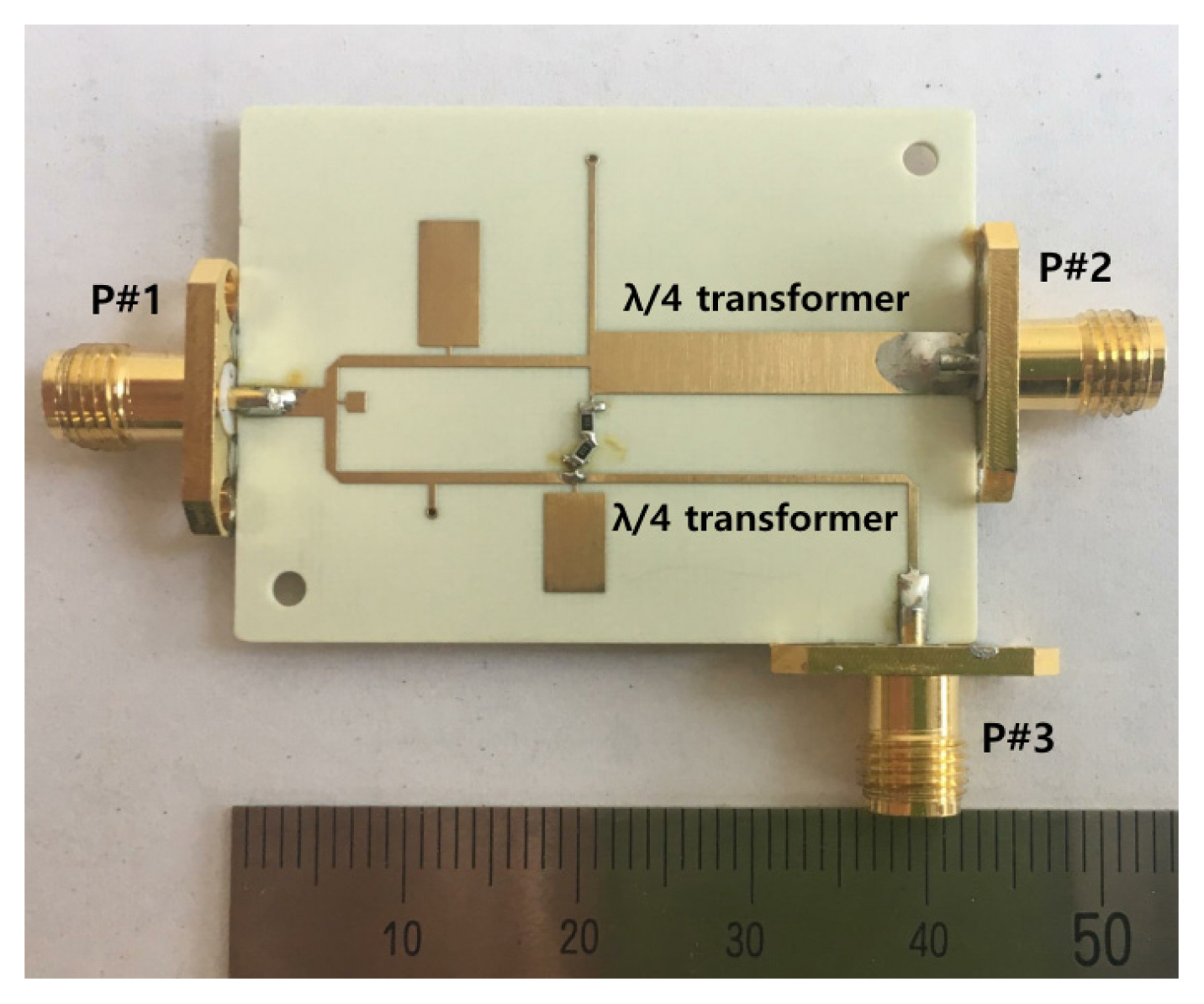
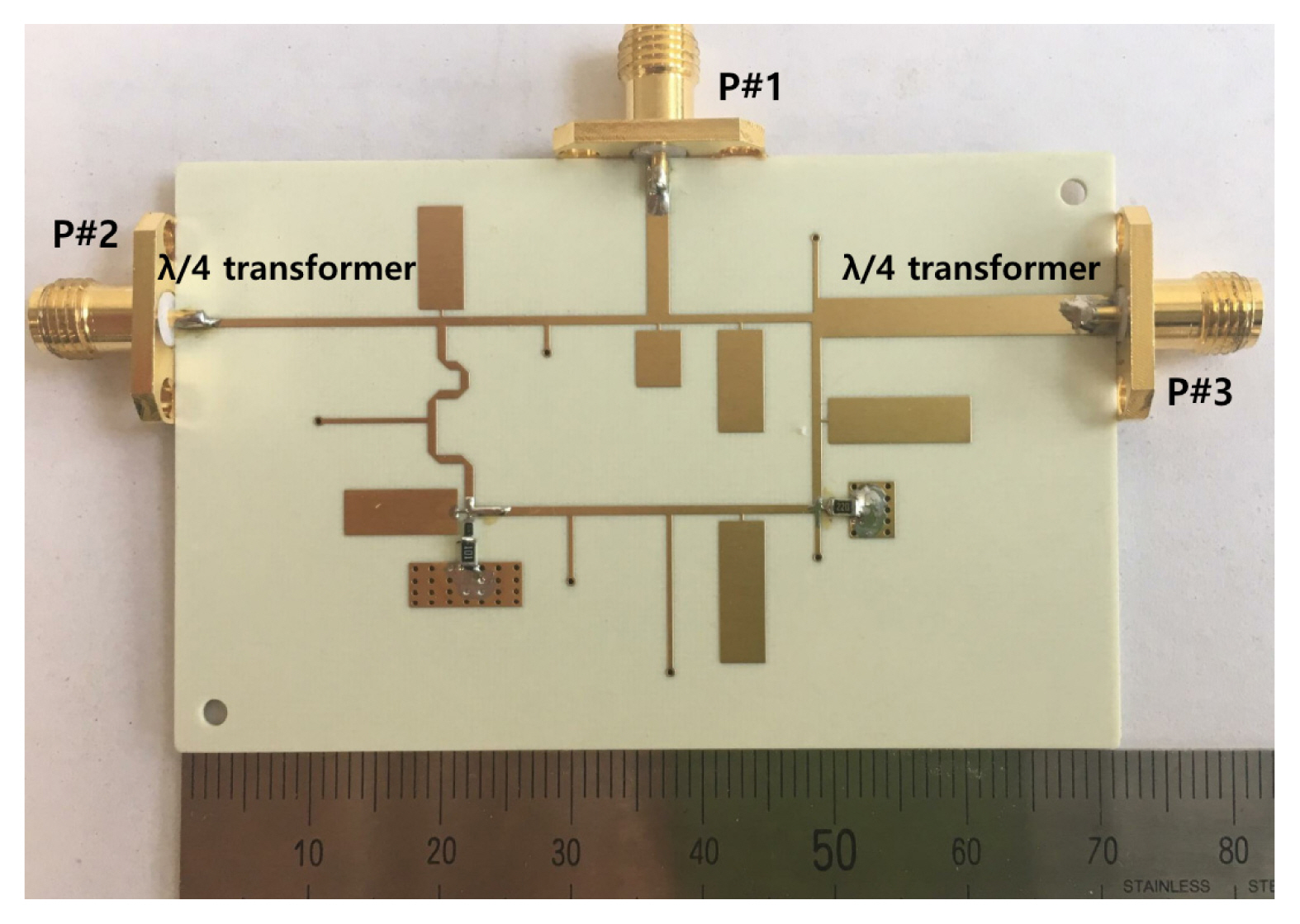
Fig. 4 depicts a photograph of the devised unequal Wilkinson power divider after the optimization process. Because there is no standard resistance value, the isolation resistance is implemented by connecting 150 ╬® and 15 ╬® in series.
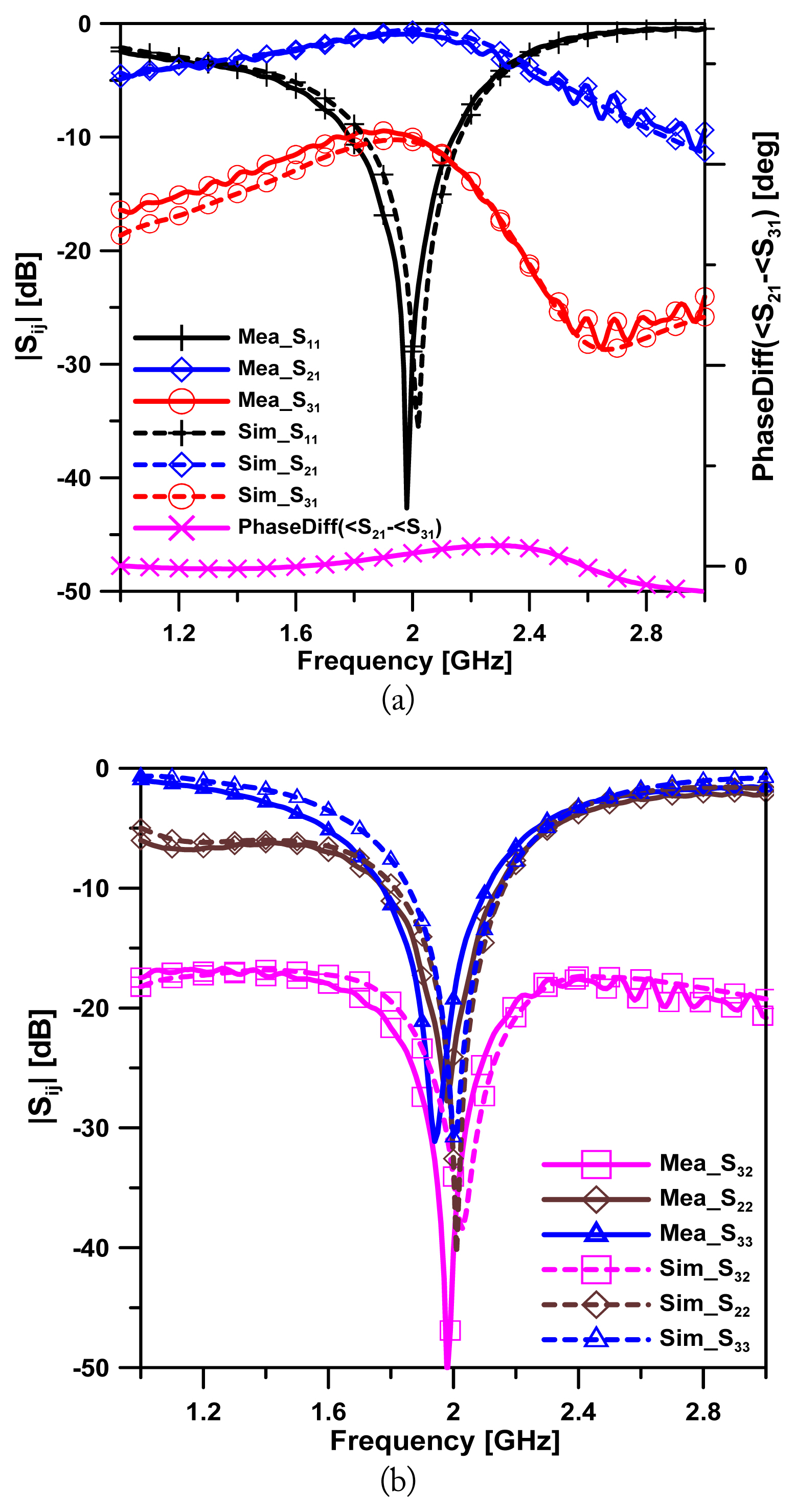
Fig. 5 shows the S-parameters of the simulated and measured unequal Wilkinson power dividers. The insertion losses of |S21| and |S31| were ŌłÆ0.96 dB and ŌłÆ10.01 dB, respectively. Furthermore, the isolation of |S32| was greater than 35 dB. The input return loss of |S11| was less than ŌłÆ25 dB and the output return losses of |S22| and |S33| were less than ŌłÆ20 dB at a center frequency of 2 GHz. The measured ŌłÆ15dB bandwidth of |S11| was in the range of 1.88 to 2.08 GHz, featuring a fractional bandwidth of 10%. In addition, the phase difference between the output ports was measured within ┬▒15┬░.
In addition, Fig. 6 depicts a photograph of the fabricated unequal Gysel power divider after the optimization process. Because there is no standard resistance value, the isolation resistance is implemented by connecting 100 ╬® and 47 ╬®, in series, and 22 ╬®.
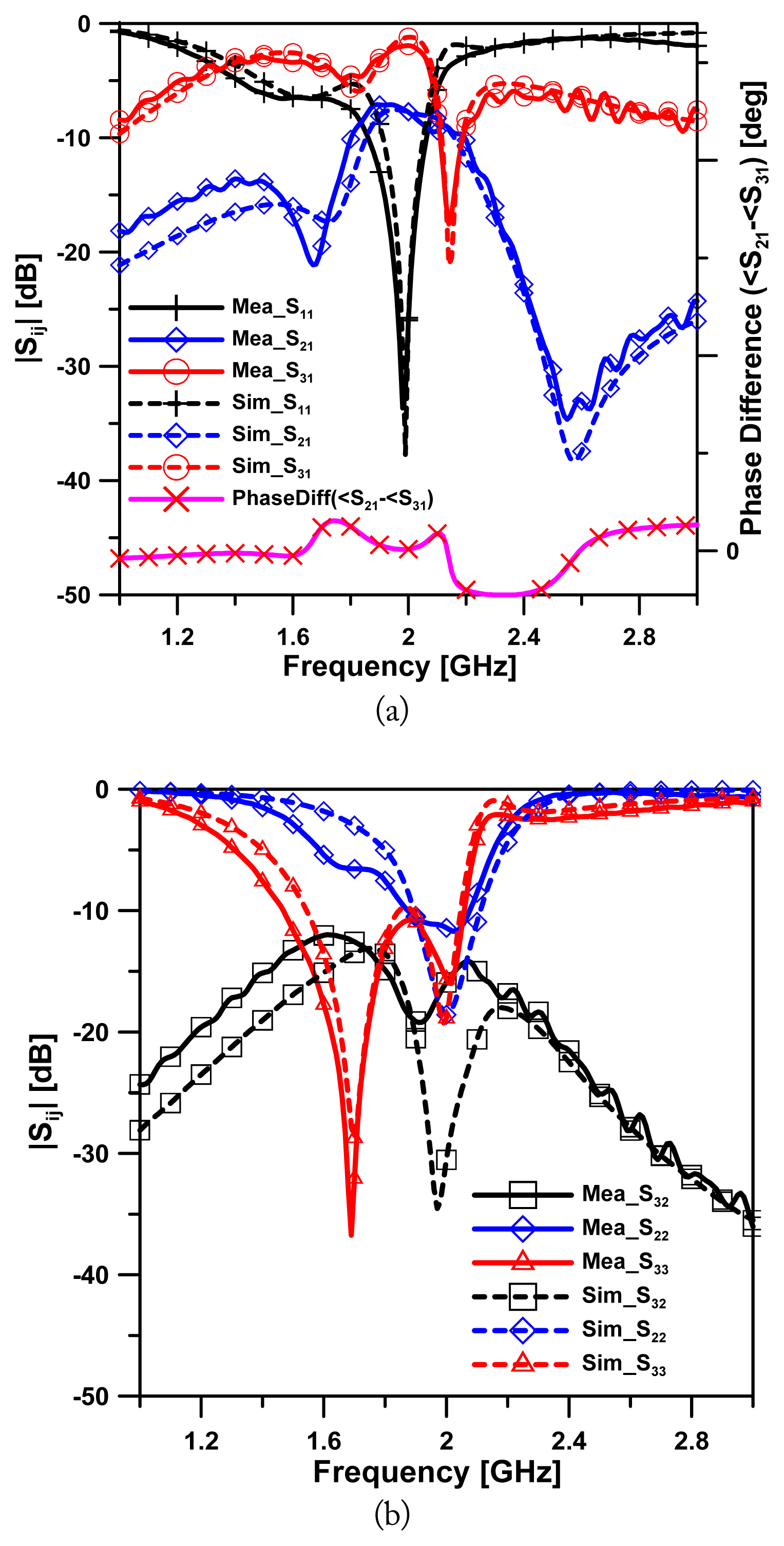
Fig. 7 displays the S-parameters of the simulated and measured unequal Gysel power dividers. The insertion losses of |S21| and |S31| were ŌłÆ1.92 dB and ŌłÆ7.74 dB, respectively. Furthermore, the isolation of |S32| was greater than 15 dB. The input return loss of |S11| was less than ŌłÆ25 dB, and the output return losses of |S22| and |S33| were less than ŌłÆ10 dB at a center frequency of 2 GHz. The measured ŌłÆ15dB bandwidth of |S11| was in the range of 1.91 to 2.03 GHz, featuring a fractional bandwidth of 6%. In addition, the phase difference between the output ports was measured within ┬▒4┬░.
IV. Conclusion
This study applied an impedance control method to the design of a Wilkinson and a Gysel power divider with splitting ratios of 9:1 and 5:1, respectively. In this method, the high impedance line was separated into two lines, and open- and short-circuit stubs were connected to three ports in parallel. This method is considerably more convenient than the conventional one using thick materials to implement high-impedance lines.
The method presented here, which can easily implement high-impedance lines, can be used for the design of various parts.