I. Introduction
Electromagnetic field transmission through a slot aperture in a conducting plate is a canonical problem that has attracted the attention of many researchers. The coupling problem of electromagnetic fields between regions through slots and apertures in conducting planes is widely encountered in electromagnetic pulse (EMP) studies and in areas of electromagnetic compatibility (EMC) and electromagnetic interference [1–5]. Another application field is microscopy, where super resolution based on near-field imaging has been investigated [6–9]. In addition, extraordinary optical transmission phenomena have been observed through a subwavelength slit, and enhanced optical transmission through multiple grooves in the vicinity of a slit has been reported for dual metal plates [10]. Electromagnetic coupling between two half-space regions separated by two slot-perforated parallel conducting screens has been reported on a transmission cross-section (TCS) [11].
Recent studies have focused on the reduction of electromagnetic penetration through narrow slots in a conducting screen, and electric shielding effectiveness has been considered for a dual plate with narrow slots [12–18]. The resonant behavior of a small aperture backed by a conducting body has been reported [19], and enhanced resonance transmission has been investigated on shaped apertures, narrow small slots, and small square slots using two parallel wires (acting as a reactance) loaded in the slot [20–26].
This study focuses on the TCS between two half-space regions separated by two narrow, small, slot-perforated parallel conducting planes. Subsequently, a formulation based on a coupled integral equation on slot aperture magnetic currents similar to Leviatan’s report [11] on a two-dimensional problem pertaining to transmission resonances is presented, which is known as the transmission resonance. In this study, the dual plate problem is addressed as a three-dimensional problem; the method of moments (MoM) using Galerkin’s procedure is used to determine the TCS through narrow small slots.
The numerical results show that the TCS of the narrow small slots between two plates became extremely small. The electromagnetic transmission through the narrow small slots cannot be large at a specified plate spacing owing to the propagated power in a region between the two plates. In this study, the enhanced characteristics of the TCS for narrow small slots on two plates were investigated using two parallel wires loaded into the slots. The maximum transmission resonance occurred when a reactance was connected to the narrow small slots for a specified plate spacing. When the plate spacing was larger than 0.5λ, the TCS was reduced to ≈90% in the single plate case, and TCS enhancement was extremely difficult. In particular, for small slots, the TCS did not increase satisfactorily because of the power propagated between the two plates. However, when the plate spacing was less than 0.5λ, the TCS decreased gradually to approximately 36% in the single plate case; TCS enhancement can then be realized using two parallel wires. The results show that the wire loaded in slot #1 is thought to play an important role in increasing the coupled power from Region I to Region II, whereas the wire loaded in slot #2 efficiently transmitted electromagnetic waves into Region III. The calculated transmission coefficient (TC) of the dual metallic wall with narrow small slots was compared with the experimental results.
II. Problem Formulation
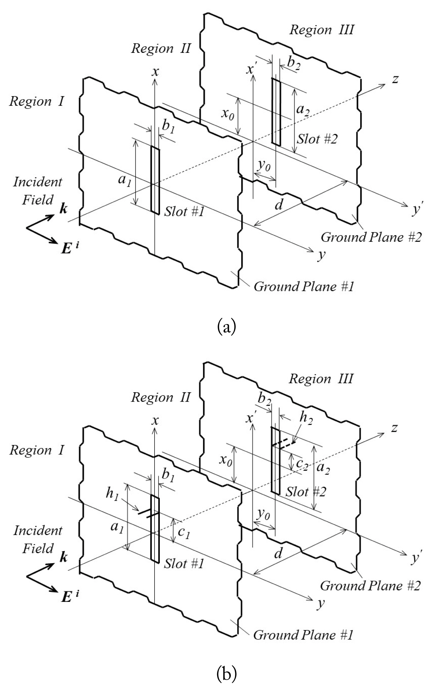
Fig. 1 shows the geometry and coordinate system of a dual conducting plane with narrow small slots. Conducting ground plane #1 was located in the xy-plane with the origin at the center of the slot aperture; ground plane #2 was placed in the xy-plane apart from ground plane #1 at a distance z = d. Narrow small slot #1 of length a1 and width b1 was placed in infinite conducting ground plane #1 at z = 0 and near slot #2 of length a2 and width b2 in infinite conducting ground plane #2, which was placed by offsets x0 and y0 from the x- and y-axes, respectively. The conducting ground planes were perfect electric conductors with zero thickness.
As shown in Fig. 1, the dual conducting wall structure was categorized into three regions: a half-space containing the incident plane wave (Region I (z < 0)), an interior region comprising the two conducting ground planes (Region II (0 < z < d)), and a half-space comprising the penetrating field (Region III (z > 0)). These three regions were assumed to be free-space regions.
If the plane wave is incident on the narrow slot in metallic ground plane #1, then the simultaneous integral equations for the unknown magnetic currents M̄1 and M̄2 on the slot apertures can be expressed as follows:
(1a)
(1b)
where
I ¯ ¯ k = ω ɛ 0 μ 0 K ¯ ¯ i j m I K ¯ ¯ i j m I I M ¯ 1 ± = ∓ z ^ × E ¯ a 1 M ¯ 2 ± = ∓ z ^ × E ¯ a 2
In Eq. (1), the incident magnetic field and current at the connecting position of the two parallel wires can be expressed as follows:
and
where H̄SC is the short-circuited magnetic field when the narrow small slot is covered by a conducting plate;
E 0 y i
To solve the simultaneous integral equations for the unknown variables, the aperture electric fields on the slots, Ēa1 and Ēa2, are expanded as follows:
where V1n and V2m are the coefficients to be determined, whereas Fn and Fm are piecewise sinusoidal expansion functions.
III. Transmitted, Propagated Power, and TCS
When a plane wave excites narrow small slot #1, the time average power transmitted from Region I to Region II through slot #1 is expressed as
where the asterisk denotes a complex conjugation. Similarly, the power transmitted from Region II to Region III through slot #2 is expressed as
In addition, the TC through narrow small slot #2 is defined as follows:
where Pinc denotes the average incident power intercepted by narrow small slot #1. For an incident plane wave,
where A is the area of aperture #2, and
H O x i
When a plane wave excites a narrow, small slot, the TCS of the narrow, small slot is defined as the area for which the incident wave contains the power transmitted by the narrow small slot. It follows that the TCS is equal to TC · A.
For a small, electrically thin antenna, the maximum absorption area (TCS) is equal to 3λ2/4π (= 2Gλ2/4π, G = 1.5); moreover, it is a Hertzian source. If the thin dipole or narrow slot resonates at near half the wavelength, then the TCS becomes 3.28λ2/4π (= 2Gλ2/4π, G = 1.64).
This study focuses on the TCS problem when all three regions are free-space regions. A method for obtaining an enhanced TCS through the two narrow small slots separated by plate spacing is demonstrated herein. The dissipated power for a lossy material filling (Region II) case will be discussed in another paper.
IV. Numerical Results and Discussion
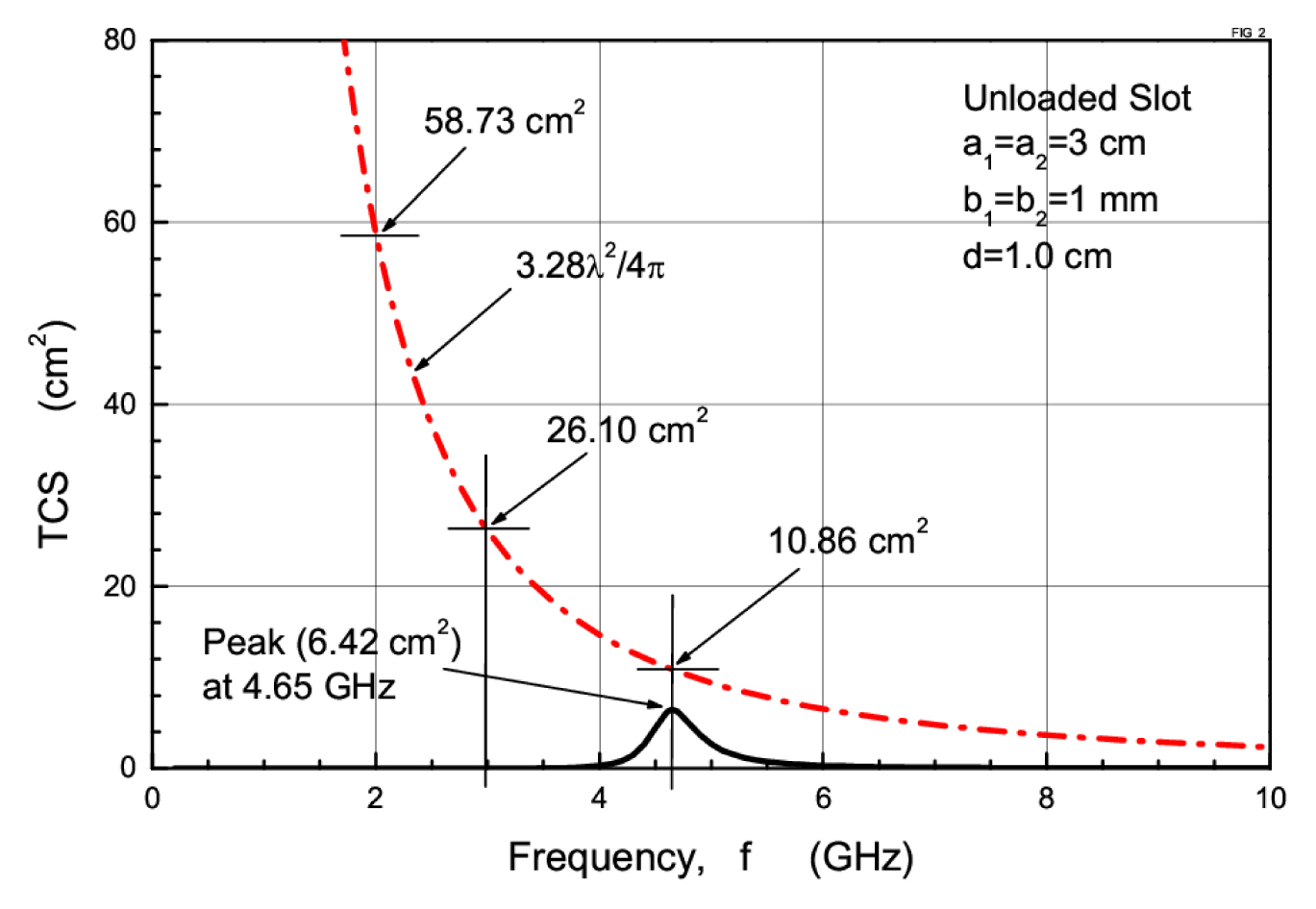
The slot used in the calculation was small and narrow compared with the wavelength. The dimensions of the slot were as follows: a1 = a2 = 3 cm, b1 = b2 = 1 mm, and d = 1 cm. Low frequencies below the resonant frequency (4.65 GHz) were used to consider the TCS of the narrow small slots. To obtain the maximum transmission, two slots were placed on the same axis (x0 = y0 = 0 cm).
Fig. 2 shows the TCS for a narrow slot with a1 = a2 = 3 cm without the two parallel wires. As shown in Fig. 2, the maximum transmission (TCS = 6.42 cm2) for a1 = a2 = 3 cm occurred at a resonant frequency of 4.65 GHz when the plate spacing was d = 1 cm. Furthermore, Fig. 2 shows that TCS = 3.28λ2/4π (= 2Gλ2/4π, G = 1.64), which is the maximum TCS (see dash-dotted lines) for the resonant source (i.e., when the narrow slot resonates at near half the wavelength). For example, the predicted maximum TCSs of the narrow slot with a1 = a2 = 3 cm were 58.73, 26.10, and 10.86 cm2 at 2, 3, and 4.65 GHz, respectively, as shown in Fig. 2. However, because the slot length was small compared with the wavelength at these frequencies, the transmission power was extremely low: TCS = 7.79 × 10⁻⁶ cm2 at 1 GHz, 2.07 × 10⁻⁴ cm2 at 2 GHz, and 0.004 cm2 at 3 GHz. The fixed plate spacing of d = 1 cm was 0.155λ at a resonant frequency of 4.65 GHz for slot lengths of 3 cm. As previously mentioned, the TCS was extremely small at 1 GHz, but it increased when the slot length was half the wavelength and the plate spacing was small. Hence, the plate spacing affected the TCS because power was propagated in Region II (between the two plates). The small plate spacing increased the TCS, as predicted.
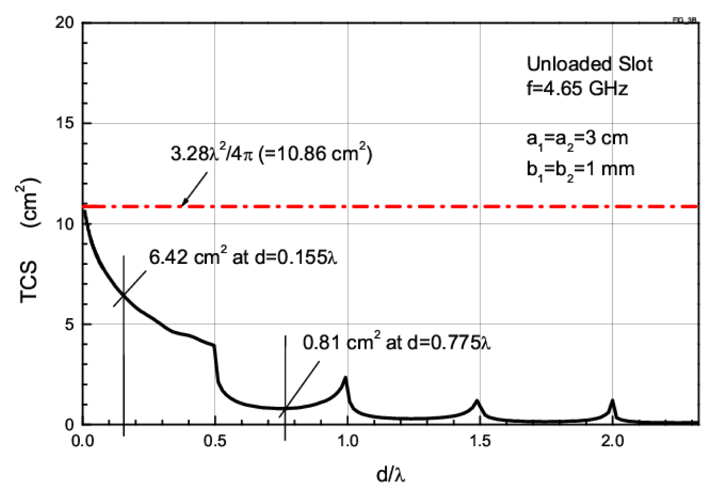
The TCS characteristics in Region III as a function of plate spacing d (or d/λ) for 4.65 GHz when the plane wave is incident to the unloaded narrow small slots of a1 = a2 = 3 cm are shown in Fig. 3. The TCS fluctuated with the plate spacing, and the fluctuation period was approximately 0.5λ; however, the TCS decreased gradually within 0.5λ. For a plate spacing exceeding 0.5λ, these periodic TCS patterns decreased rapidly as the spacing between plates #1 and #2 increased. The TCS was reduced by approximately 92.5% from the maximum owing to the propagated power in the two parallel plate regions (Region II).
However, when the plate spacing was less than 0.5λ, the TCS decreased gradually to approximately 36% in the single plate case; TCS enhancement can be realized using two parallel wires. The method by which low frequencies below the resonant frequency were transmitted from a narrow small slot with a1 = a2 = 3 cm (resonant frequency of 4.65 GHz) using two parallel wires was investigated in this study. By this wire loading procedure, the transmission can be enhanced; this enhanced transmission is called the maximum transmission (known as resonance transmission), as shown in [20, 25].
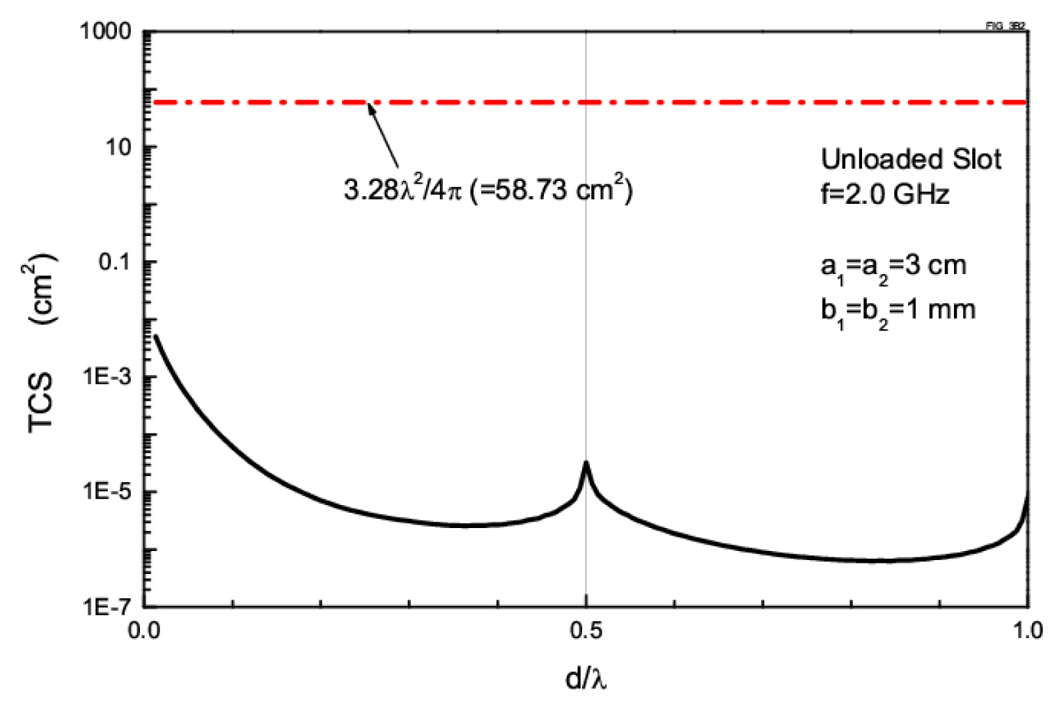
Fig. 4 shows the plate spacing characteristics of the TCS for a slot length of 3 cm at a frequency of 2 GHz. The 3-cm slot length was electrically small for this frequency. The maximum TCS (6.42 cm2) occurred at 4.65 GHz for d = 1 cm, as shown in Fig. 3. However, the TCS for 2 GHz was extremely small because the 3-cm slot length was electrically small for this frequency, as shown in Fig. 4. The frequency of 4.65 GHz corresponded to the resonance frequency of two narrow slots with a length of 3 cm, and the maximum TCS occurred at 4.65 GHz. For a slot length of 3 cm, the resonant frequency can be reduced from 4.65 GHz to various desired frequencies of 1 GHz (78.5% reduction), 2 GHz (57.0% reduction), and 3 GHz (35.5% reduction) by adding two parallel wires into the slot.
To enhance the TCS for a slot length of 3 cm at a low frequency of 2 GHz, two parallel wires can be connected to the slot. The two parallel wires serve as reactance elements. The impedance of the slot is effectively controlled by the wires, and the slot resonance occurs when the two parallel wires are adjusted to zero the slot reactance. This method has been shown to successfully enhance the TCS in a single slot [20]. In this study, two cases were addressed:
Slot #1 Loading Case: structure h1 connected to slot #1;
Slot #1 and #2 Loading Case: structures h1 and h2 connected to slots #1 and #2, respectively.
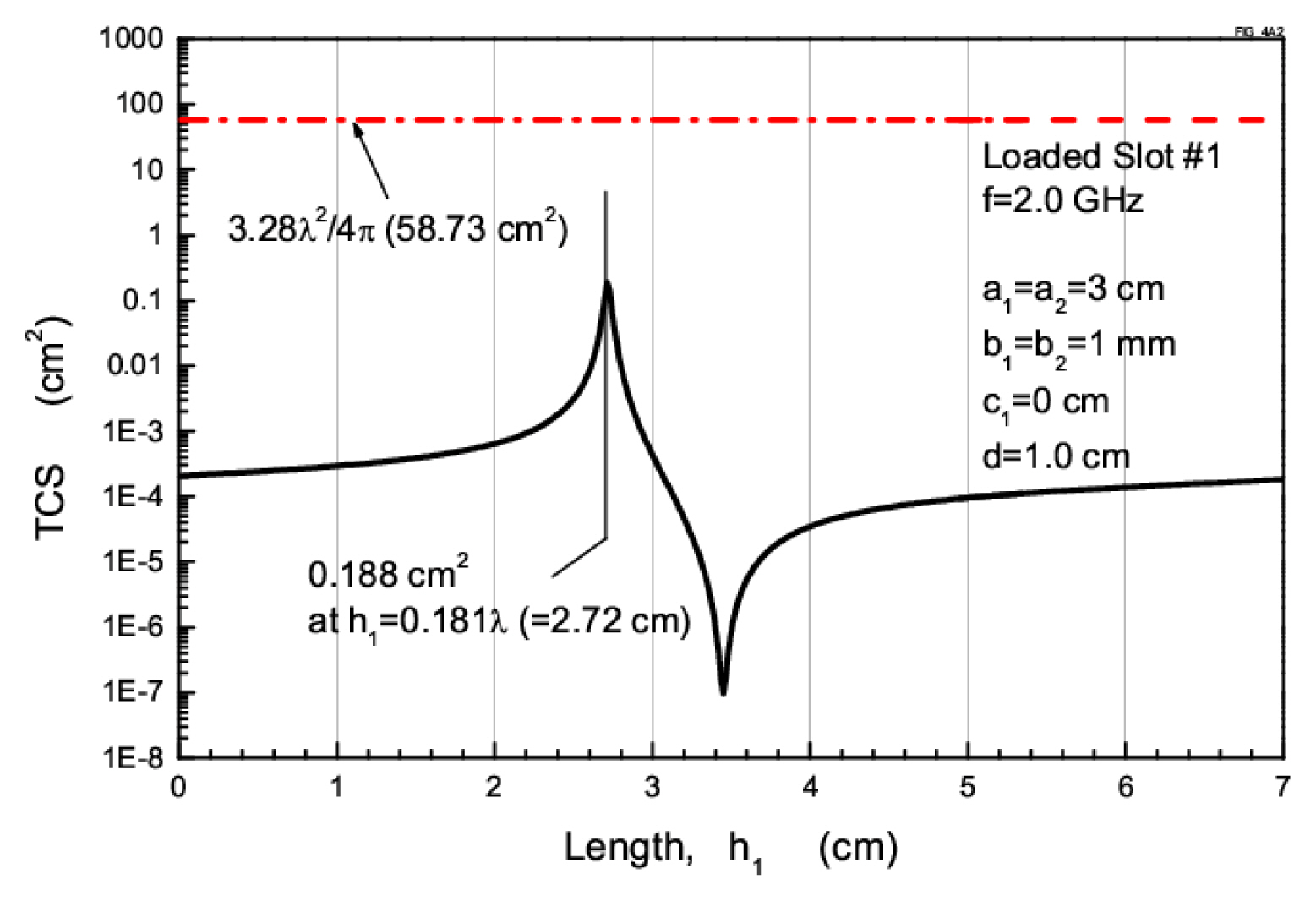
For the Slot #1 Loading Case, the TCS vs. reactance length for a 3-cm slot length at frequency 2 GHz is shown in Fig. 5. For reactance length h1 = 2.72 cm, the TCS was enhanced to 0.188 cm2 from 2.07 × 10⁻⁴ cm2, i.e., approximately 908 times larger than that of the unloaded slot at 2 GHz. Hence, the TCS can be effectively enhanced using two parallel wires connected to the slot. Adjusting the plate spacing to within 0.5λ can increase the TCS more significantly, as shown in Fig. 3.
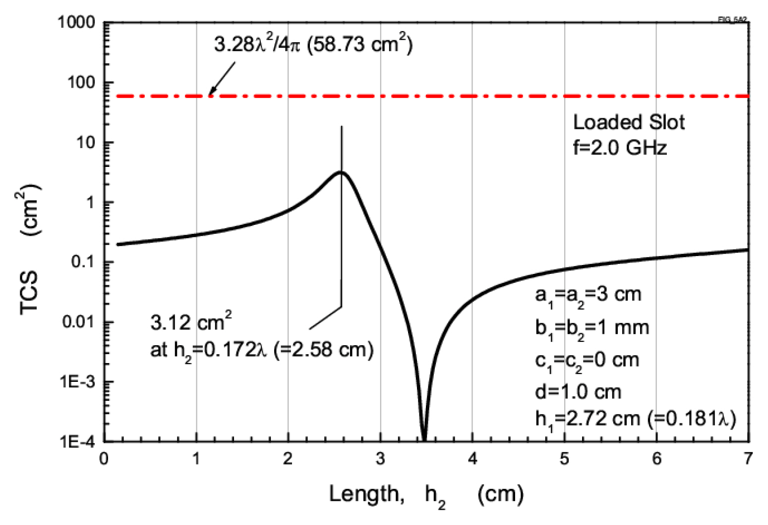
For the Slots #1 and #2 Loading Case, the TCS vs. length h2 for a 3-cm slot length at a fixed length of h1 is shown in Fig. 6. When h2 = 2.58 cm and h1 = 2.72 cm were selected, the TCS was enhanced to 3.12 cm2 from 2.07 × 10⁻⁴ cm2, i.e., approximately 15,072 times larger than that of the unloaded slot at 2 GHz. The TCS of the two slot-loaded cases (Slots #1 and #2 Loading Case) at 2 GHz became approximately 17 times that of the single loaded case (Slot #1 Loading Case). Hence, the TCS can be enhanced more effectively using the two parallel wires connected to both slots #1 and #2.
As shown in Figs. 5 and 6, when h1 = 3.450 cm and h2 = 3.480 cm, the minimum TCS was obtained at 2 GHz. The length of h1 = 3.450 cm and h2 = 3.480 cm correspond to h1 = 0.230λ and h1 = 0.232λ at 2 GHz, respectively. These results are similar to the single plate case and operate as an aperture cutoff filter. For the single plate, the penetrated electric field is reduced to zero by the two parallel wire lengths of around 0.27λ [12, 16].
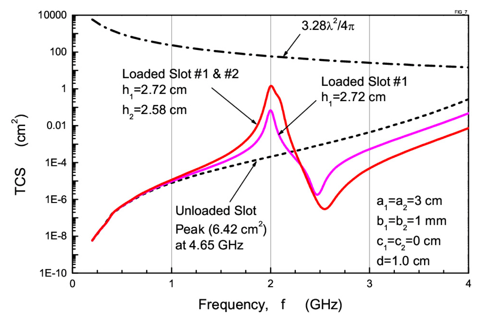
Fig. 7 shows the frequency characteristics of the TCS for a 3 cm slot length at fixed lengths of h1 and h2, which yielded the maximum TCS at the target frequency of 2 GHz. To compare the TCS for the three-case structure, the TCSs of the Unloading Slot Case, Slot #1 Loading Case, and Slots #1 and #2 Loading Case are shown in Fig. 7.
For the Slot #1 Loading Case, when h1 = 2.72 cm was selected and fixed, the maximum TCS (0.188 cm2) was obtained at 2 GHz. For the Slots #1 and #2 Loading Case, when h1 = 2.72 cm and h2 = 2.58 cm were selected and fixed, the maximum TCS (3.12 cm2) was obtained at 2 GHz. These results show that the TCSs of both slot loading cases were larger than that of the Slot #1 Loading Case.
In addition, the minimum TCS was obtained at around 2.5 GHz when h1 = 2.72 cm (= 0.227λ) and h2 = 2.58 cm (= 0.215λ), as previously explained in Figs. 5 and 6.
From the aforementioned results, it is clear that the wire loaded in slot #1 is thought to play an important role in increasing the coupled power from Region I to Region II, whereas the wire loaded in slot #2 efficiently transmitted the electromagnetic waves through slot #2 from Region II to Region III.
As shown in Fig. 7, the desired maximum TCS for a single plate was 3.28λ2/4π (= 2Gλ2/4π, G = 1.64), which was the TCS for the resonant slot near the half- wavelength. In fact, as shown in Fig. 7, the TCS of the dual plate did not reach the desired maximum TCS because of the propagated power in Region II. The differences between the desired maximum TCS (3.28λ2/4π) and actual TCS for the plate spacing are shown in Fig. 3. Therefore, for a specified plate spacing, the maximum TCS can be effectively obtained using parallel wires loaded in the slot. In addition, a smaller plate spacing increased the TCS.
The TCS in Region II was not considered in this study because the TCS characteristics for Region III focused primarily on power transmission applications and EMC problems.
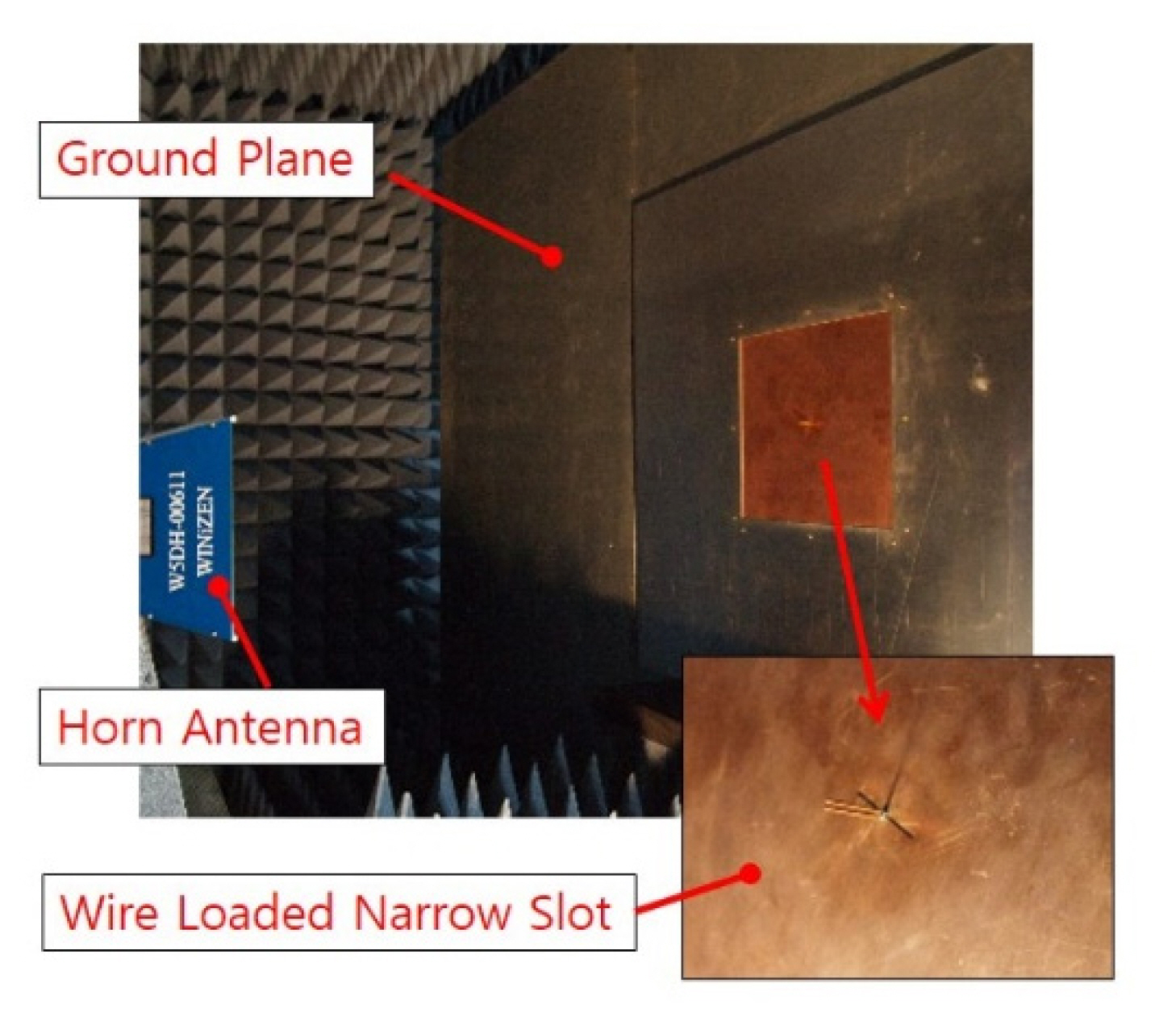
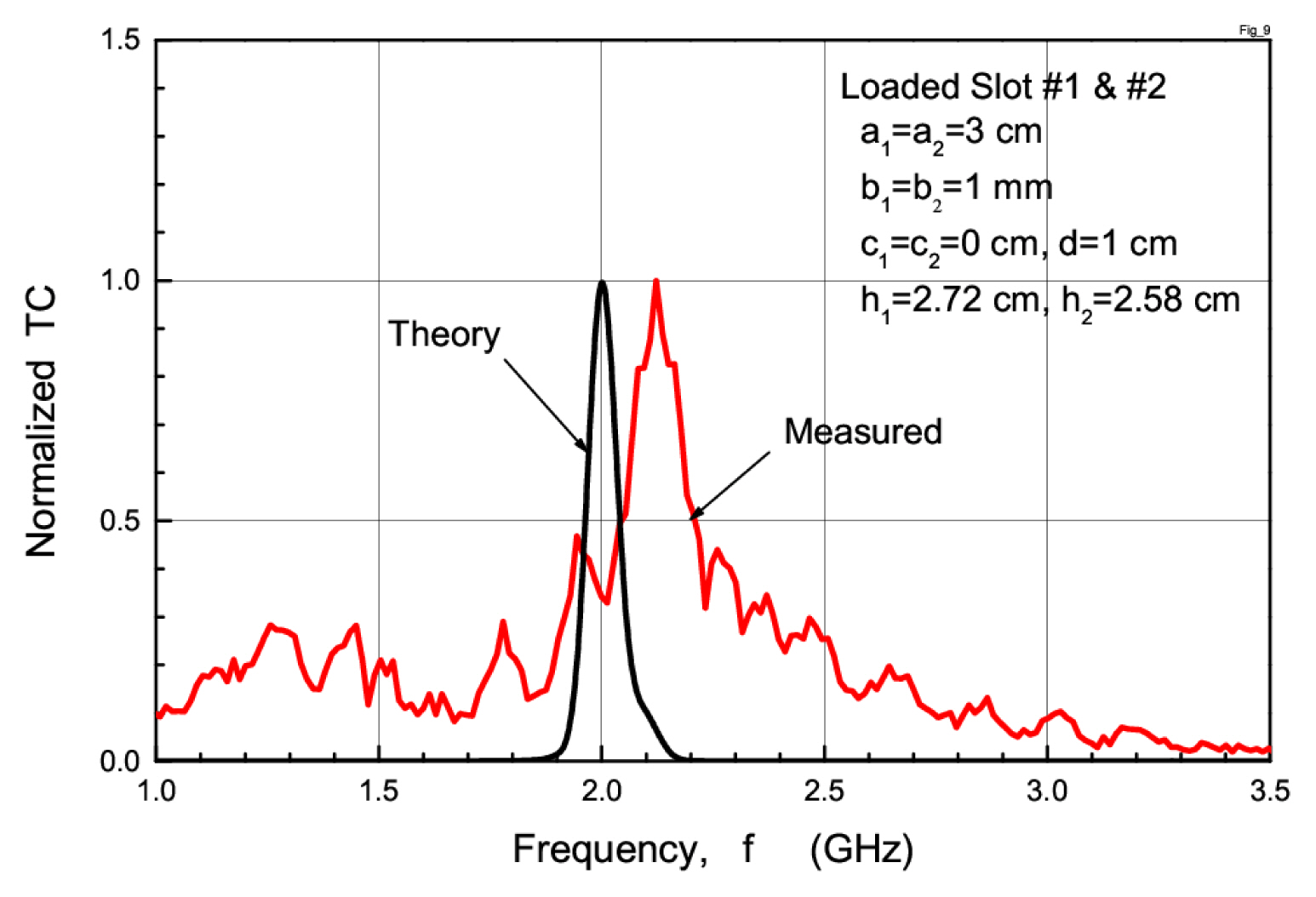
Experimental results are provided to validate the numerical calculations. Fig. 8 shows a photograph of the experimental setup for measuring the transmission characteristics of the dual-plate slot-loaded structure. Two small narrow slots (3 cm × 1 mm) were attached to two large ground planes (2 m × 4 m and 1 m × 1 m) with a gap of 1 cm in an anechoic chamber. Two parallel wires with a radius of 0.5 mm made from copper were connected at the center of the narrow slot as a capacitive reactance. Broadband double-ridged horn antennas made by the ICU (model No. ICU-MA-04-2, 0.75-6 GHz) were used as the transmitting and receiving antennas. The S-parameters were measured by the antennas under a normal incidence using a Wiltron 37225A vector network analyzer. The antennas were placed 150 cm away from the structure to satisfy the far-field condition.
Fig. 9 shows a comparison of the experimental and theoretical results. The calculated TCs agreed relatively well with the measured data. The maximum deviation of the frequency was approximately 6%. In addition, inherent fluctuations remained in the measurements. The fluctuations and deviations were attributed mainly to the mutual coupling effects between the antenna and slot as well as the interactions between the transmitting horn antenna and ground plane.
V. Conclusion
TCS characteristics from an incident plane wave penetrating narrow small slots in dual conducting planes were explained herein. An analysis was performed wherein integral equations for aperture electric fields were derived and solved by applying Galerkin’s MoM. For two slots with an electrically small length, a high-level TCS, known as the transmission resonance, was obtained for a plate spacing within 0.5λ. The analysis results demonstrated that the maximum transmission resonance occurred effectively when using two parallel wires loaded into both slots instead of a single slot loading for a small plate spacing. The wire loaded in slot #1 is thought to play an important role in increasing the coupled power from Region I to Region II, whereas the wire loaded in slot #2 efficiently transmitted electromagnetic waves into Region III, as a result of which a significant increase in the total TCS results was seen in the experimental results.