J. Electromagn. Eng. Sci Search

CLOSE


J. Electromagn. Eng. Sci > Volume 21(5); 2021 > Article
Ramakrishna, Satish Kumar, and Reddy: Quadruple Band-Notched Compact Monopole UWB Antenna for Wireless Applications

Abstract

A printed quadruple band-notched ultra-wideband (UWB) antenna characteristic is presented. The designed UWB antenna has a size of 32 mm × 30 mm × 1.6 mm and covers an impedance bandwidth off 2.9–14.5 GHz for the entire frequency band. The entire frequency band maintains voltage standing wave ratio (VSWR) < 2, except at WiMAX (3.1–3.6 GHz), WLAN (4.92–6.12 GHz), downlink of X-band for satellite communication systems (7.5–8.4 GHz), and X-band (10.2–11 GHz). By inserting a pair of L-shaped slots into the radiating element, a H-shaped resonator and rectangular split-ring resonators are closely arranged to the microstrip feed-line, alongside the measured impedance bandwidth of 129%. The fabricated antenna radiation pattern and return loss is presented.

I. Introduction

Recently, ultra-wideband (UWB) antenna technology has had considerable growth. Nevertheless, various demands for fashioning the full potential of this technology still exist. UWB technology is the most promising wireless technology for the future: imaging systems, high data rates, radar, and high precision. Researchers are increasingly interested in UWB antennas due to their many applications. From the literature survey, various techniques for designing UWB antennas through band notches have been discussed. To improve UWB antennas’ bandwidth, single- and double-band notch characteristics are conducted using a T-shaped slot two I-shaped slots, Γ-shaped stubs, and customized G-slot defected ground structure (DGS) employed within the ground plane, radiating patch, and feed line, correspondingly [1]. There are many methods to notch bands from the UWB impedance bandwidth. In addition, parasitic elements were introduced near the monopole patch to reject existing bands. The circular disk monopole antenna comprises three patches, in which the outer patches separate the unwanted bands from the impedance bandwidth [2]. It means patches work as band-stop filters over the entire impedance frequency band. By incorporating a quarter wavelength of stubs on the bottom plane and close to the microstrip feed line of the antenna, it achieved a UWB band. The center frequency of the notch band changes with the physical dimensions of the stubs [3]. Compact printed triple notched antenna was analyzed by altering the affective dimensions of the stubs, and the band-notched characteristics were conducted by introducing slots on the patch and the bottom plane [4].
UWB characteristics were achieved by establishing a pair of spur lines in the microstrip feed line [5] and split ring resonators [6] used to suppress existing systems [7] from the UWB antenna impedance bandwidth. Different methods have been used to reject unwanted frequency bands from the UWB by placing slots, slits [8], and stubs with different shapes arranged in a radiating patch and feed line. Single, dual, triple, and quadruple notches removed from the UWB antenna have been achieved by placing different slots, such as ring slot, tapered slot [9], antipodal tapered slot [10], U-shaped slot, non-uniform short-circuited stub [11], T-shaped slot [12] etched in the radiating element, and bottom plane [13]. In addition, different stubs [14], uni-planar differentially driven elements [15], and open loop resonators [16] were also used to achieve notches from the UWB antenna impedance bandwidth.
Similarly, notches were achieved using a non-uniform stub resonator, rectangular stub [17], H-shaped resonator [18], split-ring resonator on radiator [19], rectangular split-ring resonator [20], U-shaped stub in stepped slot [21], elliptic single complementary split-ring resonators [22], electric ring resonator (ERR) with coplanar waveguide (CPW) structure [23], two pairs of DGS resonator-shaped slits [24], and L-shaped slits [25]. CPW fed [26] UWB using slots with a dimension of quarter wavelength, tri-arm resonator [27], stepped impedance resonator [28], meander ground-defects [29], one trim-arm filter, folded planar monopole [30], metallic pins [31], curved tapered slots [32], and filter on feed line used for notch-existing wireless communication systems from the UWB band.
In this study, a quadruple band-notched compact UWB antenna with slots and resonators is proposed. An antenna can achieve voltage standing wave ratio (VSWR) < 2 over an entire impedance bandwidth of 2.9–14.5 GHz by etching triangle-shaped cuts on the ground plane and radiating patch. By incorporating a pair of L-shaped slots on the radiating element, a H-shaped resonator, and adding a rectangular split-ring resonator near the microstrip feed line, quadruple-notched UWB antenna characteristics can be achieved. An antenna is analyzed from the surface currents, and changing the dimensions of the slots and resonators requires frequency band-notch achieved from the UWB band. The simulated results of the proposed quadruple band-notched UWB antenna align with the measured results.

II. Design and Analysis of the Presented Antenna

1. Antenna Structure

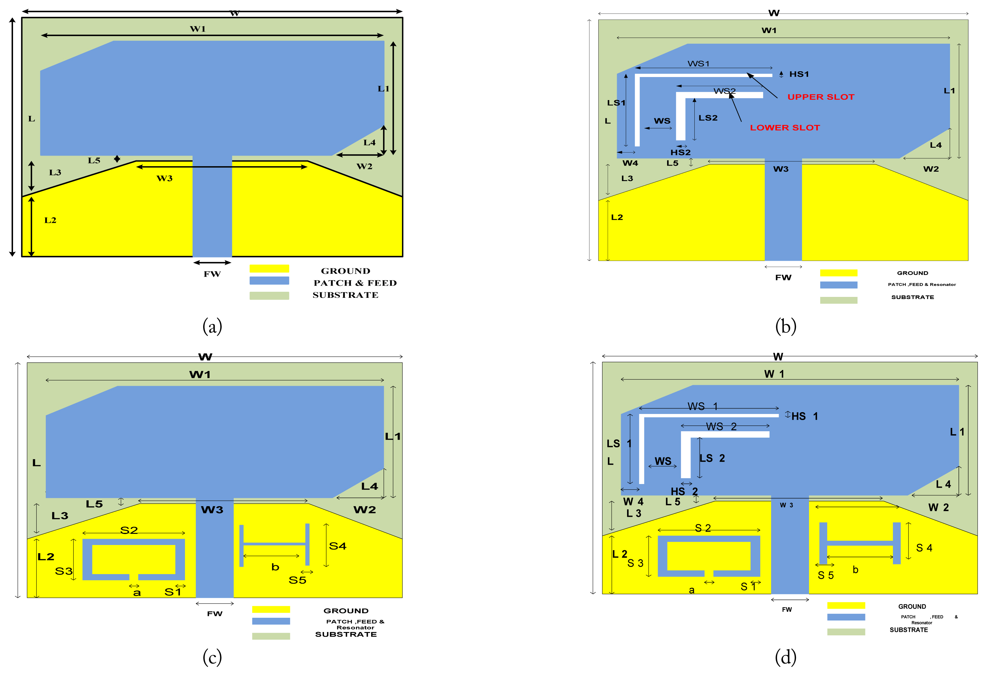
The presented antenna has a size of 32 mm × 30 mm and is placed on the FR4 epoxy substrate with a thickness of 1.6 mm. Fig. 1(a) shows that a 50-Ω feed line feeds the UWB antenna; it contains the patch with triangular cuts and defective ground structure. The antenna parameters are optimized with a high frequency structured simulator. Finally, simulated values (in mm) are specified below: FW = 4.1, W = 30, L3 = 6.5, L4 = 7.5, W1 = 26.4, W2 = 7.2, W3 = 15, L = 32, L1 = 18.4, L2 = 4.5, and L5 = 0.5.
Fig. 1(b) shows the proposed UWB antenna micro-strip line aligned with an impedance matching radiating element. It contains a radiating element among a pair of triangular cuts with L-shaped slots, and a defective ground structure along a pair of triangular cuts is used for dual-band notches. The presented UWB antenna parameters are optimized with a high frequency structured simulator. Finally, simulated values (in mm) are specified below: FW = 4.1, W = 30, W1 = 26.4, W2 = 7.2, W3 = 15, L = 32, L1 = 18.4, L2 = 4.5, L5 = 0.5, WS1 = 14, LS1 = 12, WS2 = 11.5, LS2 = 11, HS1 = 0.5, HS2 = 1, WS = 2.5, W4 = 1.4, L3 = 6.5, and L4 = 7.5. Fig. 1(c) shows the presented UWB antenna and micro-strip lines with impedance matching, and it contains a radiating element among a pair of triangular cuts, and a defective ground structure, alongside a H-shaped resonator and rectangular split-ring resonators, is used for dual-band notches. The antenna parameters are optimized with a high frequency structured simulator. Finally, simulated values (in mm) are specified below: FW = 4.1, W = 30, W1 = 26.4, W2 = 7.2, W3 = 15, L = 32, L1 = 18.4, L2 = 4.5, L5 = 0.5, S2 = 6, S3 = 5, S1 = 0.5, a = 3, S4 = 4.4, S5 = 0.5, b = 3.7, L3 = 6.5, and L4 = 7.5.
Fig. 1(d) shows the presented UWB antenna and micro-strip lines with impedance matching, and it contains a radiating patch with a pair of triangular cuts, and a defective ground structure, alongside H-shaped and rectangular ring resonators and two L-shaped slots, is used for quadruple band notches. The antenna parameters are optimized with a high frequency-structured simulator. Finally, simulated values (in mm) are specified below: FW = 4.1, W = 30, W1 = 26.4, W2 = 7.2, W3 = 15, L = 32, L1 = 18.4, L2 = 4.5, L5 = 0.5, WS1 = 14, LS1 = 12, WS2 = 11.5, LS2 = 11, HS1 = 0.5, HS2 = 1, WS = 2.5, W4 = 1.4, S2 = 6.5, S3 = 6, S1 = 0.5, a = 3, S4 = 4.5, S5 = 0.5, b = 2.9, L3 = 6.5, and L4 = 7.5.
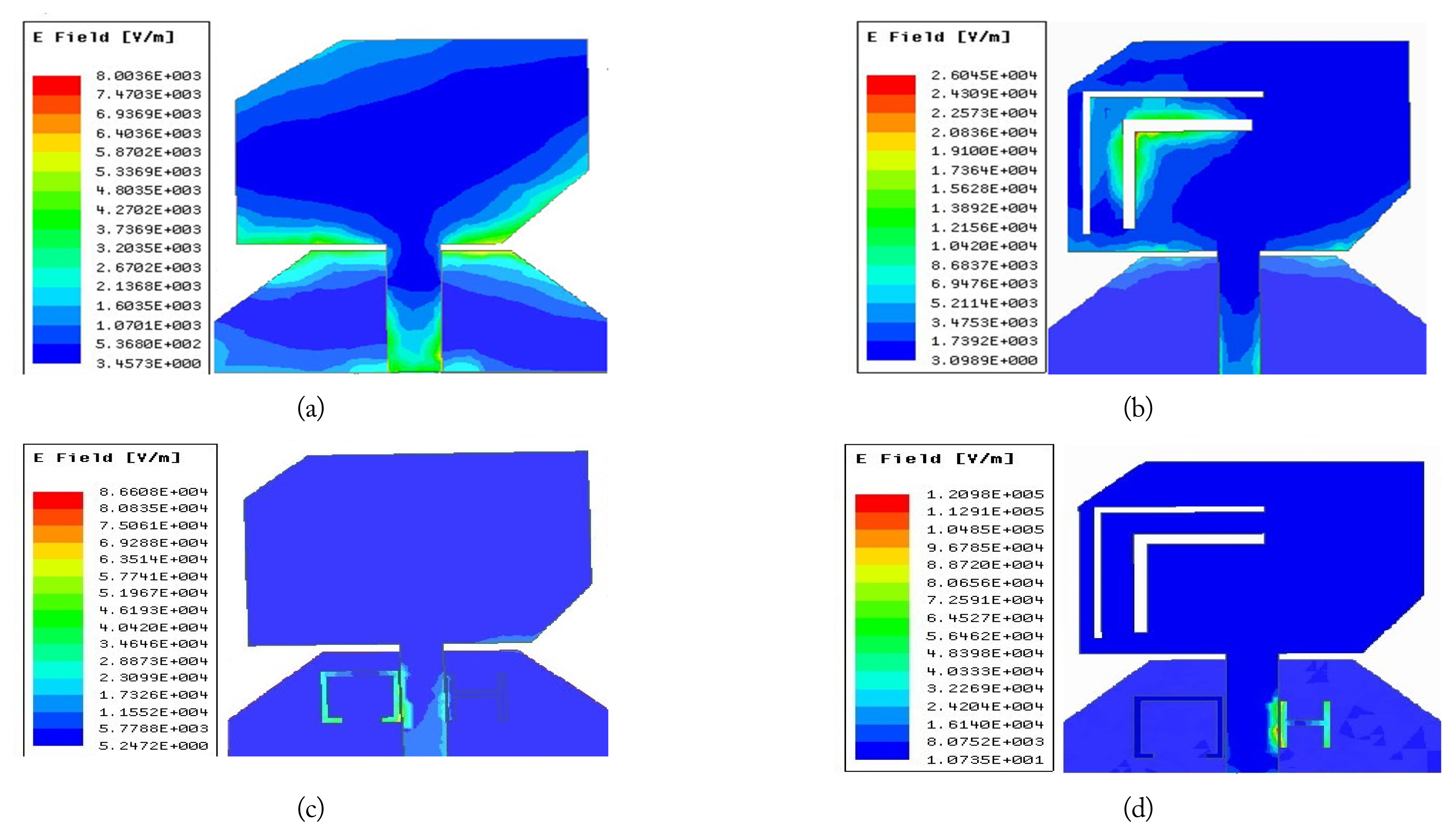
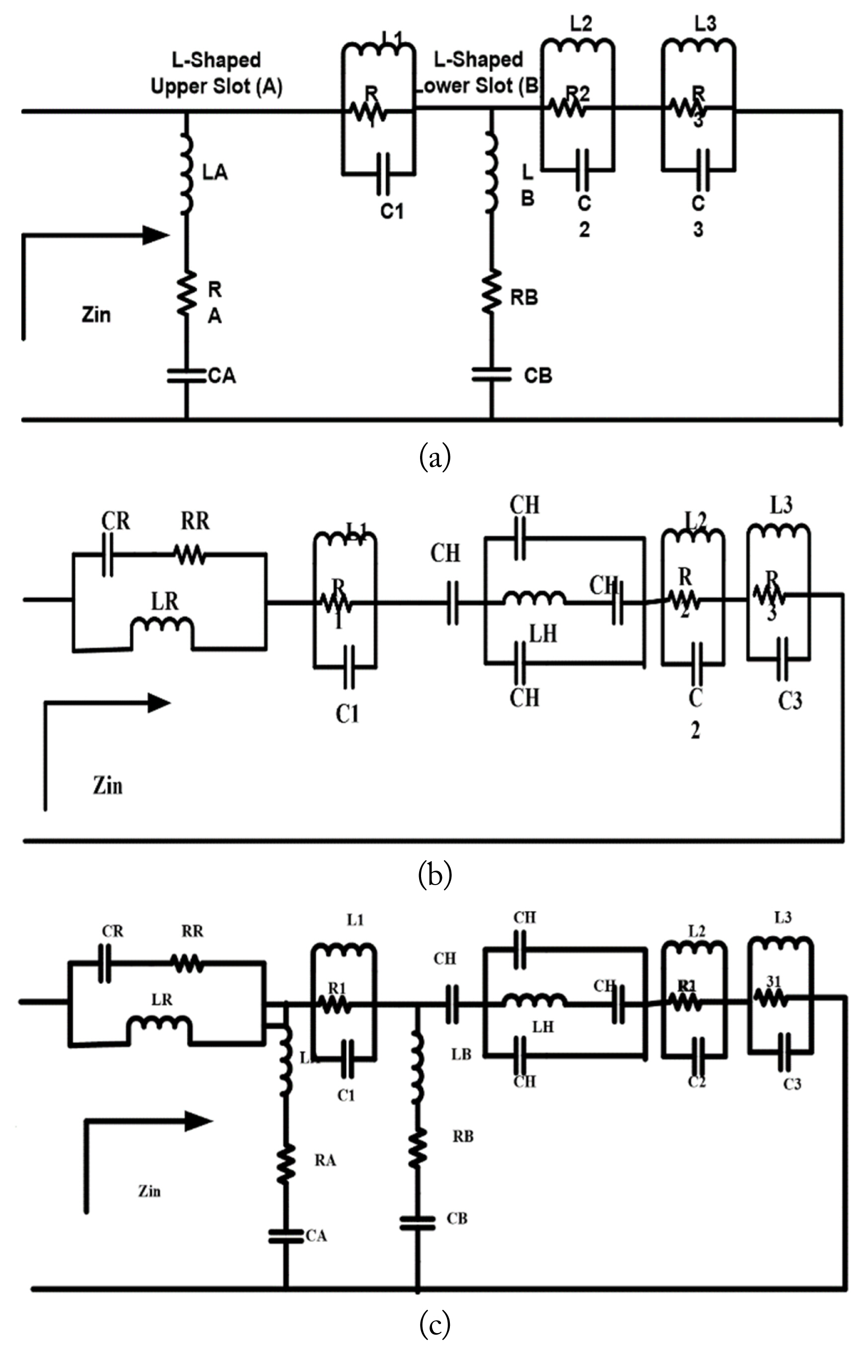
Fig. 2(a) shows the current distribution on the radiating element of the evolutionary process of a quadruple band-notched compact UWB antenna structure. Initially, it means that before placing L-shaped slots on the patch, there is a high current density at the bottom edge and sides of the radiating patch and a very low current distribution at the center of the radiating element. Consequently, it is clear that the performance of the antenna is deficient because of the low surface current density at the center of the proposed UWB antenna. Therefore, the notches for mitigating interference can easily get involved in the radiating patch without affecting the actual performance of the presented UWB antenna. Fig. 2(b) shows the strongest surface current distribution alongside the slots. Because of the different values of WS1 of the upper L-shaped slot, the surface current distribution also changes correspondingly, and a band notch occurs at WiMAX. Similarly, for the different WS2 values of the lower L-shaped slot, the current density varies accordingly. From the slots loaded on the radiating patch taken as a capacitive reactance, it was observed that the slot width increased as the resonant frequency decreased. The UWB antenna extends beyond resonances in the entire range of operation. Fig. 3(a) shows the dual-notched UWB antenna equivalent circuit with a pair of L-shaped slots in the radiating rectangular patch. Similarly, Fig. 3(b) and 3(c) show the proposed dual-notched UWB antenna equivalent circuit with H-shaped and rectangular split-ring resonators and a pair of L-shaped slots arranged beside the microstrip feed line and in the radiating patch, respectively.
Where LA, RA, and CA and LB, RB, and CB are the circuit parameters of the upper L-shaped slot and the lower L-shaped slot on the radiating patch, correspondingly. The circuits are responsible for wireless local area network (WLAN) and WiMAX notch bands in a UWB band. The remaining parallel resonating circuit elements L1, R1, C1, R2, L2, C2, R3, L3, and C3 are used to enhance antenna bandwidth. Similarly, from Fig. 3(b) and 3(c), the CR, RR, and LR and CH and LH are the circuit parameters of the rectangular split ring resonator and H-shaped split ring resonators responsible for satellite communications and X-Band notch bands in the UWB band, correspondingly.

2. Design Process

The design process of the antenna explained the four development iterations of the compact UWB antenna. First, Fig. 1 shows the UWB Antenna-1. Second, to suppress the existing narrow bands, WiMAX and WLAN from the radiating patch, two L-shaped slots are etched, as shown in the Antenna-2 of Fig. 1. The length for the upper L-shaped slot and lower L-shaped slots are 26 mm, 22.5 mm, and 0.5 mm width for the upper and lower L-shaped slots, respectively. Third, to suppress the existing narrow bands of WLAN and satellite communications, H-shaped and rectangular split-ring resonators are arranged beside the feed line, as shown in Antenna-3 of Fig. 1. Finally, to suppress WiMAX, WLAN, satellite communications, and X-Band from the presented antenna, two L-shaped slots and two resonators with different dimensions are arranged in the patch and near the microstrip feed line, respectively.

3. Notched Mechanism

Fig. 2 shows the current distribution of the proposed quadruple band-notched compact UWB antenna. Antenna-2 of Fig. 1 shows the maximum current distribution around the L-shaped slots when the antenna is excited by a port and terminated with a 50-Ω load. Similarly, Antenna-3 of Fig. 2 shows most of the current around the resonators. Finally, Antenna-4 of Fig. 2 shows most of the current around the H-shaped resonator and some of the currents around the two L-shaped slots and rectangular split-ring resonator.

4. Structure Study

Fig. 4(a) shows the curve of S11 among different feed widths (FW). It can be seen that the change in feed line width of the proposed notch-band UWB antenna regarding return loss also changes. From Fig. 4(b) and 4(c), the variation curve of S11 with WS1 will affect the center frequency of the WiMAX. In contrast, the WLAN center frequency remains unchanged, and WS2 affects the WLAN center frequency, while the WiMAX center frequency remains unchanged.
The upper and lower L-shaped slots are responsible for the WiMAX and WLAN bands. The slots act as half-guided wavelength resonators for the band-notched designs. The length of the L-shaped slots can be calculated as
Lus=2[Ws1+Ls1+2Hs1],Lls=2[Ws2+Ls2+2Hs2].
Fig. 4(b) shows the return loss for the WS1 variation while keeping all other parameters constant. It was observed that the center of the band-notched frequency shifts from 3.6 to 3.1 GHz as the WS1 value increases from 11 to 13 mm. The resonant frequencies of the upper and lower slots are given by
fus=c2Lusɛreff,fls=c2Llsɛreff.
The effective dielectric constant is 2.2 for the FR4 material due to the defective ground structure.
Fig. 4(c) shows the return loss for the WS2 variation while keeping all other parameters are constant. The center of the band-notched frequency shifts from 6.12 to 4.92 GHz as the value of WS2 increases from 9 to 11 mm.
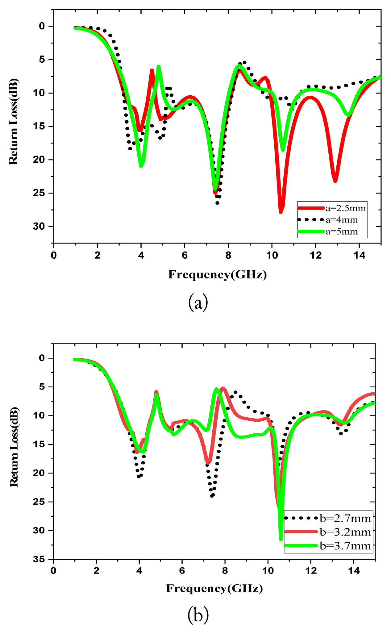
Fig. 5(a) and (b) show that the variation curve of S11 with “a” will affect the WLAN center frequency. In contrast, satellite communication center frequency remains unchanged, and variation “b” affects the satellite communication center frequency, while the WLAN center frequency remains unchanged.
The notch frequency f0, which corresponds to the rectangular split-ring resonator resonant frequency, is given by
f0=W02π=12πLTCeq,
where LT is the total length of the resonator and Ceq is the equivalent capacitance.
Ceq=[(2(S2)+S3-a)+2(S1+a)]C0,Ln=[4(2(S2)+S3)-2(S1+a)],C0=[4aavg-S1]Cpul,Cpul=ɛrv0Z0,Z0=120πɛreff.
Fig. 5(a) shows the return loss for the variation a while keeping all other parameters constant. The center of the WLAN band-notched frequency shifts from 5.5 to 4.5 GHz as the value of a increases from 2.5 to 5 mm.
The notch frequency f0, which corresponds to the H-shaped resonator resonant frequency, is given by
f0=12πLTCeq,LT=[(2(S4)+b)],Ceq=[S4+2(S5+b)]C0,C0=[4savg-S1]Cpul,Cpul=ɛrv0Z0,Z0=120πɛreff.
Fig. 5(b) shows the return loss for the variation b while keeping all other parameters constant. It is observed that the center of the satellite communication system band-notched frequency shifts from 8.4 to 7.5 GHz as the value of b increases from 2.7 to 3.7 mm.
From Fig. 6(a)–6(d), the variation curve of S11 with WS1, WS2, a, and b will affect the center frequency of WiMAX, WLAN, satellite communication, and X-band correspondingly. In contrast, other bands’ center frequencies remain unchanged.

III. Results and Discussion

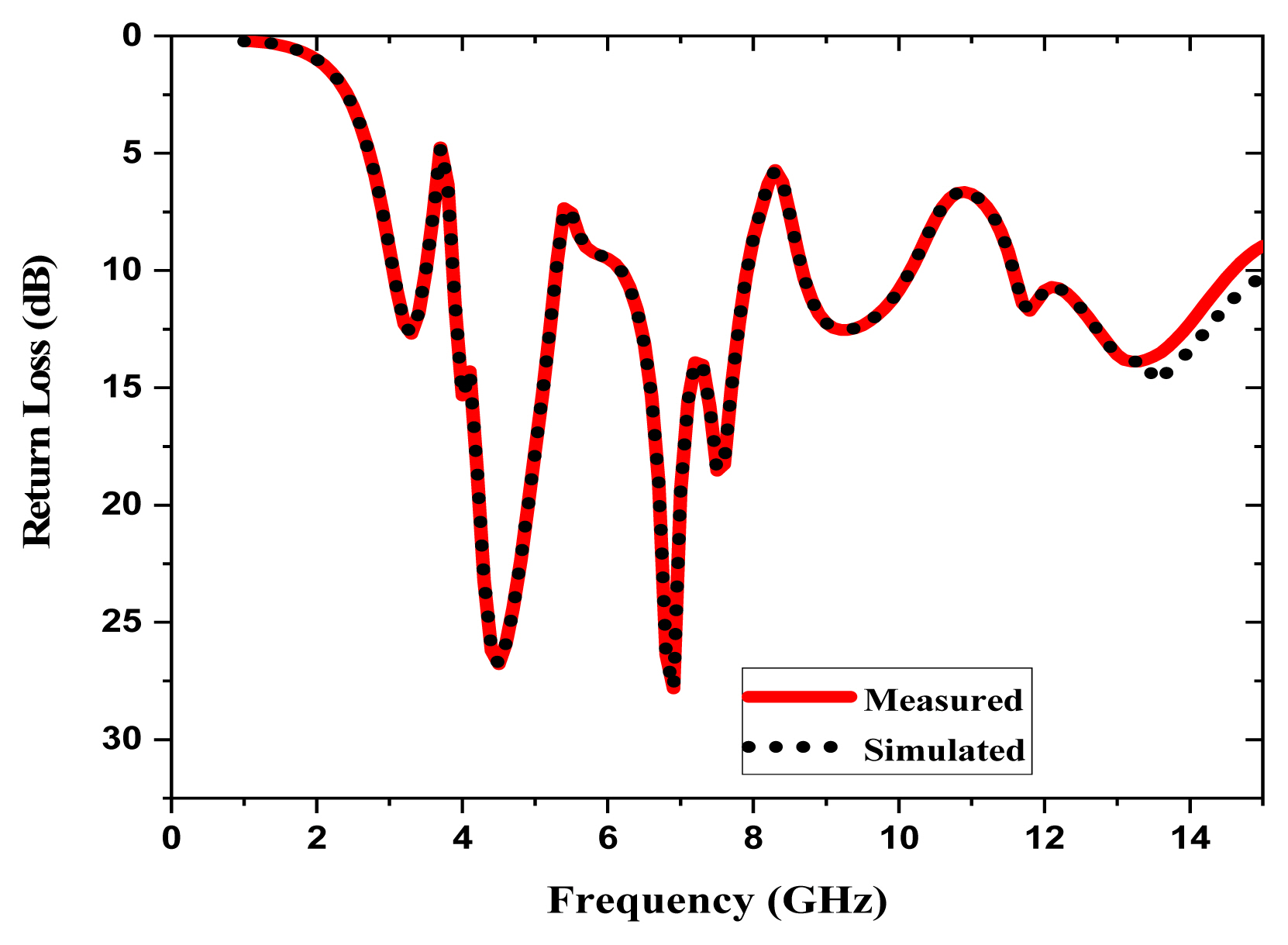
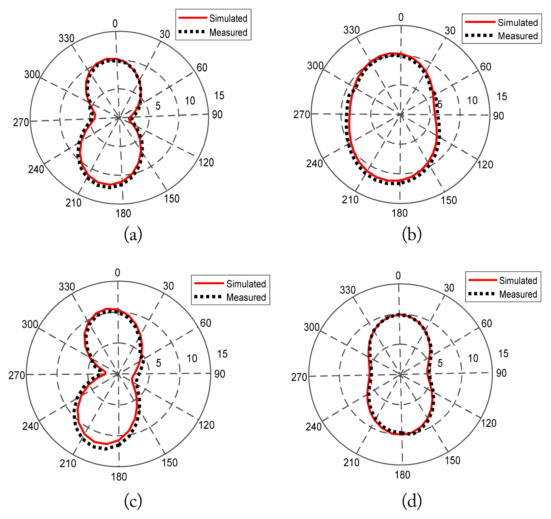
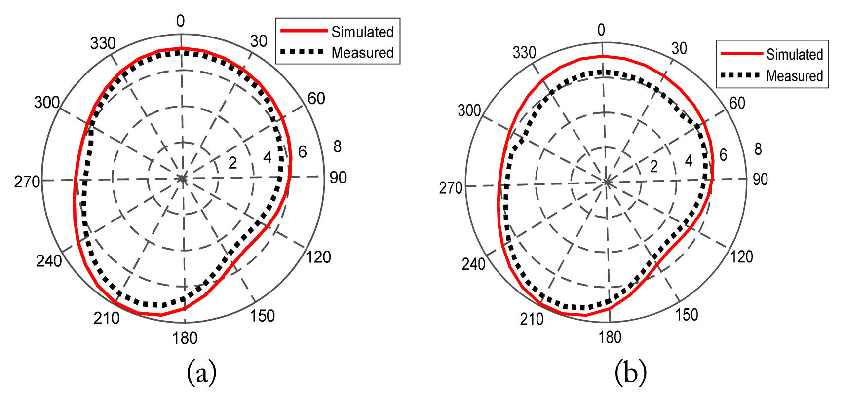
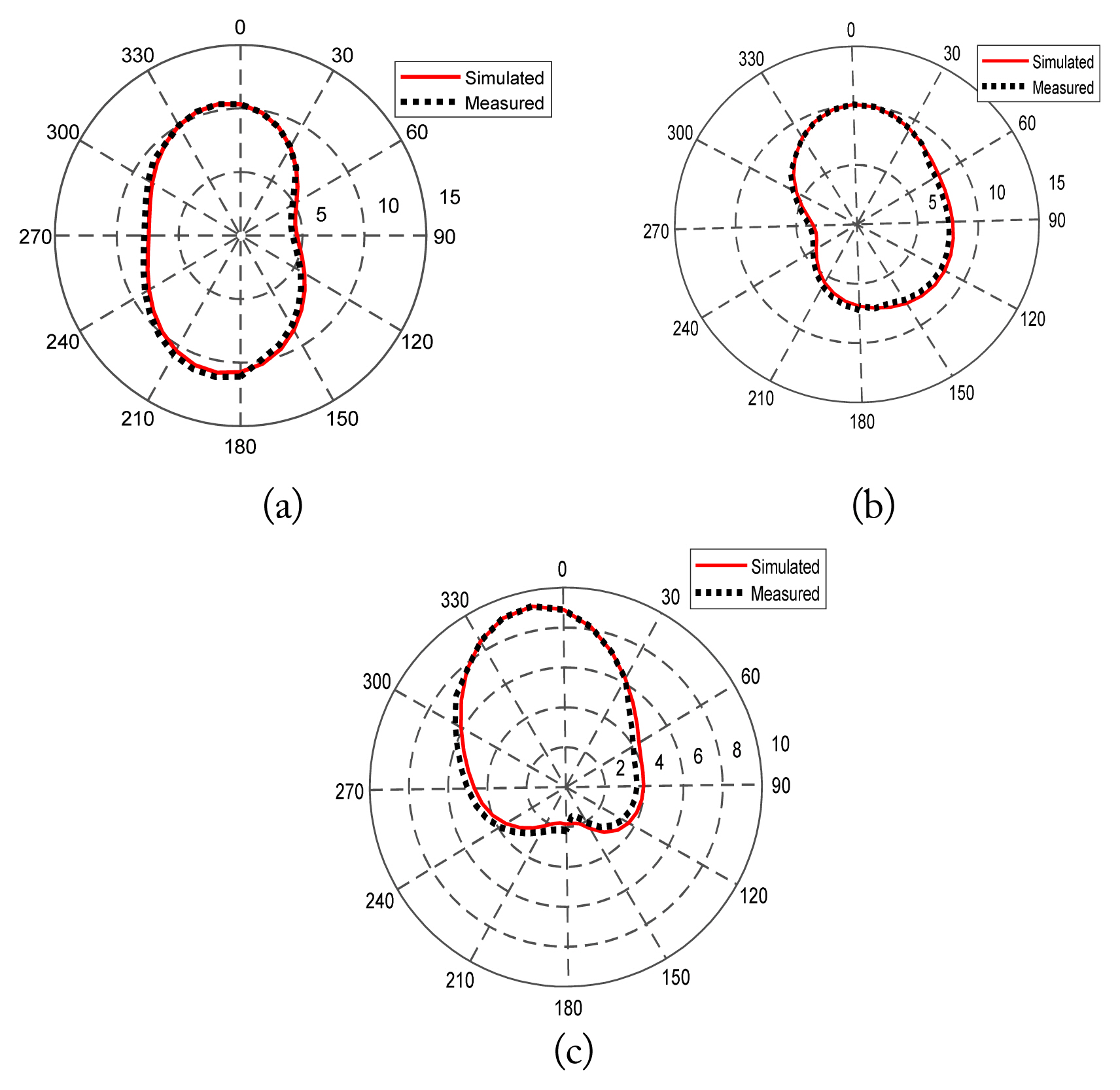
The proposed quadruple band-notched compact UWB antenna- measured radiation patterns properly agree with the simulated results. Fig. 7 shows the experimental S-parameter (S11) curve. The simulated results from Fig. 7 parallel the measured results. Figs. 8 and 9 show Antenna-1 and Antenna-2, E-plane and H-plane radiation patterns at 5 GHz, respectively. Radiation pattern is one of the basic properties of an antenna, which shows how the energy distributes in space. In Fig. 8, it is observed that the E-plane radiation pattern is quasi-omnidirectional, and the H-planes radiation patterns are the same as monopole. Fig. 9 shows Antenna-3, E-plane and H-plane radiation patterns, respectively. Figs. 10 and 11 show Antenna-4, E-plane, and H-plane radiation patterns at 5 GHz, 6 GHz, and 8 GHz, respectively.
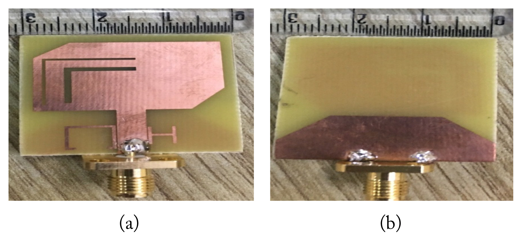
The presented antenna has an impedance bandwidth from 2.9 to 14.5 GHz through quadruple band notches at WiMAX (3.1–3.6 GHz), WLAN (4.9–6.1 GHz), satellite communications (7.5–8.4 GHz), and X-band (10.2–11 GHz). Table 1 shows a comparison between the proposed antenna and the existing antennas. Fig. 12 shows the fabricated antenna’s front and rear view. Fig. 13 shows radiation pattern measurement setup of Antenna-1 and Antenna-2 in anechoic chamber, respectively.

IV. Conclusion

A quadruple band-notched compact UWB antenna was presented and fabricated. The measured impedance bandwidth of the quadruple band-notched compact UWB antenna ranged from 2.9 GHz to 14.5 GHz alongside four-notched bands covering 3.1–3.6 GHz, 4.9–6.1 GHz, 7.5–8.4 GHz, and 10.2–11 GHz. Moreover, the antenna-notched mechanism was analyzed using the current on the surface of the patch and resonators. The variation in notched characteristics was studied using a pair of L-shaped slots and resonators. The measured return loss and radiation patterns paralleled the simulated results. This proposed quadruple band-notched compact UWB antenna is suitable for wireless applications.

Fig. 1
Development process of the presented UWB antenna: (a) Antenna-1, (b) Antenna-2, (c) Antenna-3, and (d) Antenna-4.
jees-2021-5-r-49f1.jpg
Fig. 2
Surface current distributions at 5 GHz: (a) Antenna-1, (b) Antenna-2, (c) Antenna-3, and (d) Antenna-4.
jees-2021-5-r-49f2.jpg
Fig. 3
Equivalent circuit diagram for UWB antenna with L-shaped slots, rectangular split ring resonator, and H-shaped resonator: (a) Antenna-2, (b) Antenna-3, and (c) Antenna-4.
jees-2021-5-r-49f3.jpg
Fig. 4
Variation of return loss with different dimensions: (a) S11 with different FW at Antenna-1, (b) S11 with different WS1 at Antenna-2, and (c) S11 with different WS2 at Antenna-2.
jees-2021-5-r-49f4.jpg
Fig. 5
Variation of return loss with different dimensions: (a) S11 with different a at Antenna-3 and (b) S11 with different b at Antenna-3.
jees-2021-5-r-49f5.jpg
Fig. 6
Variation of return loss with different dimensions: (a) S11 with different WS1, (b) S11 with different WS2, (c) S11 with different “a,” and (d) S11 with different “b” at Antenna-4.
jees-2021-5-r-49f6.jpg
Fig. 7
Variation curve of S11 for the proposed Antenna-4 measured and simulated results.
jees-2021-5-r-49f7.jpg
Fig. 8
Simulated and measured radiation patterns at 5 GHz: (a) E-plane and (b) H-plane of Antenna-1, (c) E-plane and (d) H-plane of Antenna-2.
jees-2021-5-r-49f8.jpg
Fig. 9
Simulated and measured radiation patterns at 5 GHz. (a) E-plane and (b) H-plane of Antenna-3.
jees-2021-5-r-49f9.jpg
Fig. 10
Simulated and measured E-plane patterns of Antenna-4 at (a) 5 GHz, (b) 6 GHz, and (c) 8 GHz.
jees-2021-5-r-49f10.jpg
Fig. 11
Simulated and measured H-plane patterns of Antenna-4 at (a) 5 GHz, (b) 6 GHz, and (c) 8 GHz.
jees-2021-5-r-49f11.jpg
Fig. 12
Fabricated antenna front view (a) and rear view (b).
jees-2021-5-r-49f12.jpg
Fig. 13
Radiation pattern measurement setup of Antenna-1 (a) and Antenna-2 (b).
jees-2021-5-r-49f13.jpg
Table 1
Proposed antenna compared with existing antennas
Study Size (mm3) Notch bands covered (GHz) Technique Frequency range (GHz)
Abdollahvand et al. [1] 20 × 18 × 1.86 3.3–3.8
5.1–6
Etching I-shaped slots on the ground plane and pair of Γ-shaped stubs 2.8–11.8
Zhang et al. [2] 47 × 37 × 1.5 5.1–6.1 Segmenting a circular patch into three parts 2.8–13.5
Taheri et al. [3] 23 × 28 × 0.8 At 3.5 and 5.8 L-shaped with quarter wavelength stubs and slot with octagonal shape 3.1–11
Nguyen et al. [4] 25 × 29 × 0.8 3.3–3.7
5.15–5.825
7.25–7.75
A straight open-ended quarter wavelength slot and semi-circular half-wavelength cut 3–11
Lee et al. [5] 29.38 × 28.25 × 0.508 5.01–6.19 λ/4 slotted line resonator and stub loaded circular radiating patch 2.95–10.75
Li et al. [6] 38.5 × 46.4 × 1 5–5.5
7.2–7.6
Etching one quasi complementary SRR in feed line and TM-MTM 2–12.5
Yang et al. [7] 25 × 30 × 0.762 NA Coplanar slot line transition 3.1–10.6
Tang et al. [8] 39 × 39 × 1.6 3.25–3.75
5.08–5.9
7.06–7.95
Multi slot and multi-slit 2.3–13.75
Tu et al. [9] 35 × 30 × 0.8 5.2–6 Pair of stubs and slits 2.78–12.3
Siddiqui et al. [10] 307.4 × 282 × 1.575 At 2.55 and 3.18 Square split-ring resonators 0–9
Chuamg et al. [11] 27.6 × 30 × 0.4 5.15–5.95 Non-uniform short-circuited stub 2.4–11
Kang et al. [12] 38.5 × 38.5 × 1.6 5.03–5.97 L-shaped slits 3.08–11.8
Jiang and Che [13] 59 × 73 × 0.8 3.3–4
5.05–5.9
U-shaped parasitic strips with T-shaped stub 2.8–11
Kingsly et al. [14] 30 × 25 × 1.57 3.31–3.57
5.26–5.45
5.78–5.91
J-shaped and asymmetric T-shaped with open-ended stub 3.1–10.6
Huang et al. [15] 64 × 64 × 0.8 5–6 Octagonal shaped slot 3–11
Gao et al. [17] 48 × 48 × 0.8 5.1–6 Two SRR slots on the radiator with 45° and two stair-cases shaped radiating element 2.5–12
Sung [18] 33 × 25 × 1.14 3.37–3.8
4.26–5.85
5.1–6
H-shaped resonator 3.04–11.3
Li et al. [20] 26 × 26 × 0.762 5.3–5.8
7.85–8.55
Split-ring resonator 2.9–11.6
Liu and Tu [21] 44 × 44 × 1.6 5.10–5.95 U-shaped feed line and slot 2.95–10.8
Sarkar et al. [22] 35 × 19 × 1.6 3.3–3.8
5.15–5.65
7.9–8.4
Elliptical single complementary split-ring resonators 2.21–11.71
Vendik et al. [23] 50 × 50 × 1.52 At 3.5, 5.8, 7.5 Electric ring resonator incorporated into the CPW 2.5–12
Chandel et al. [25] 18 × 34 × 1.6 5.1–5.8
6.7–7.1
Inverted L-shaped slits 2.93–20
Nguyen et al. [26] 19 × 24 × 1.2 3.3–3.7
5.15–5.825
7.25–7.75
Open-ended quarter wavelength slots 2.45–10.65
Azim et al. [27] 29 × 20.5 × 1.6 At 3.5 and 5.5 Dual-band notch achieved by the tri-arm resonator 2.98–10.76
Sung [28] 25 × 33 × 0.3 3.41–3.68
5.37–6.01
Two short circuits folded stepped impedance resonator 3.07–10.61
Rehman and Alkanhal [29] 80 × 70 × 1.54 2.15–2.65
3–3.7
5.45–5.98
8–8.68
Deflection slots 1.5–12
Jiang et al. [30] 200 × 200 × 1 0.72–2.96
3.25–3.59
5.06–6.21
MIMO array 3D U-slot cut 0.5–7
Zhang et al. [31] 19 × 19 × 0.6 2.4–2.5
5–10
Stub triangular shorted structure & two parasitic metallic pins 2.96–14.5
Pan and Dong [32] 80 × 80 × 0.5 NA Two tapered slots 2.94–10.06
Proposed work 32 × 30 × 1.6 3.1–3.6
4.92–6.12
7.5–8.4
10.2–11
Inserting L-shaped slots in radiating patch and H and RSRR are arranged near to feed line. 2.9–14.5

References

1. M Abdollahvand, G Dadashzadeh, and D Mostafa, "Compact dual band-notched printed monopole antenna for UWB application," IEEE Antennas and Wireless Propagation Letters, vol. 9, pp. 1148–1151, 2010.
crossref
2. K Zhang, Y Li, and Y Long, "Band-notched UWB printed monopole antenna with a novel segmented circular patch," IEEE Antennas and Wireless Propagation Letters, vol. 9, pp. 1209–1212, 2010.
crossref
3. MMS Taheri, HR Hassani, and A Nezhad, "UWB printed slot antenna with Bluetooth and dual notch bands," IEEE Antennas and Wireless Propagation Letters, vol. 10, pp. 255–258, 2011.
crossref
4. TD Nguyen, DH Lee, and HC Park, "Design and analysis of compact printed triple band-notched UWB antenna," IEEE Antennas and Wireless Propagation Letters, vol. 10, pp. 403–406, 2011.
crossref
5. CH Lee, JH Wu, G Hsu, HL Chan, and HH Chen, "Balanced band-notched UWB filtering circular patch antenna with common-mode suppression," IEEE Antennas and Wireless Propagation Letters, vol. 16, pp. 2812–2815, 2017.
crossref
6. WT Li, YQ Hei, W Feng, and XW Shi, "Planar antenna for 3G/Bluetooth/WiMAX and UWB applications with dual band-notched characteristics," IEEE Antennas and Wireless Propagation Letters, vol. 11, pp. 61–64, 2012.
crossref
7. Y Yang, Z Zhao, X Ding, Z Nie, and QH Liu, "Compact UWB slot antenna utilizing traveling-wave mode based on slotline transitions," IEEE Transactions on Antennas and Propagation, vol. 67, no. 1, pp. 140–150, 2019.
crossref
8. Z Tang, X Wu, J Zhan, S Hu, Z Xi, and Y Liu, "Compact UWB-MIMO antenna with high isolation and triple band-notched characteristics," IEEE Access, vol. 7, pp. 19856–19865, 2019.
crossref
9. ZH Tu, WA Li, and QX Chu, "Single-layer differential CPW-fed notch-band tapered-slot UWB antenna," IEEE Antennas and Wireless Propagation Letters, vol. 13, pp. 1296–1299, 2014.
crossref
10. JY Siddiqui, C Saha, C Sarkar, LA Shaik, and M Antar, "Ultra-wideband antipodal tapered slot antenna with integrated frequency-notch characteristics," IEEE Transactions on Antennas and Propagation, vol. 66, no. 3, pp. 1534–1539, 2018.
crossref
11. CT Chuang, TJ Lin, and SJ Chung, "A band-notched UWB monopole antenna with high notch-band-edge selectivity," IEEE Transactions on Antennas and Propagation, vol. 60, no. 10, pp. 4492–4499, 2012.
crossref
12. L Kang, H Li, X Wang, and X Shi, "Compact offset microstrip-fed MIMO antenna for band-notched UWB applications," IEEE Antennas and Wireless Propagation Letters, vol. 14, pp. 1754–1757, 2015.
crossref
13. W Jiang and W Che, "A novel UWB antenna with dual notched bands for WiMAX and WLAN applications," IEEE Antennas and Wireless Propagation Letters, vol. 11, pp. 293–296, 2012.
crossref
14. S Kingsly, D Thangarasu, M Kanagasabai, N Alsath, SK Palaniswamy, TR Rao et al., "Tunable band-notched high selective UWB filtering monopole antenna," IEEE Transactions on Antennas and Propagation, vol. 67, no. 8, pp. 5658–5661, 2019.
crossref
15. H Huang, Y Liu, S Zhang, and S Gong, "Uniplanar differentially driven ultrawideband polarization diversity antenna with band-notched characteristics," IEEE Antennas and Wireless Propagation Letters, vol. 14, pp. 563–566, 2015.
crossref
16. J Deng, S Hou, L Zhao, and L Guo, "A Reconfigurable Filtering Antenna With Integrated Bandpass Filters for UWB/WLAN Applications," IEEE Transactions on Antennas and Propagation, vol. 66, no. 1, pp. 401–404, Jan;2018;PMID: 10.1109/TAP.2017.2760363.
crossref
17. P Gao, S He, X Wei, Z Xu, N Wang, and Y Zheng, "Compact printed UWB diversity slot antenna with 5.5-GHz band-notched characteristics," IEEE Antennas and Wireless Propagation Letters, vol. 13, pp. 376–379, 2014.
crossref
18. Y Sung, "Triple band-notched UWB planar monopole antenna using a modified H-shaped resonator," IEEE Transactions on Antennas and Propagation, vol. 61, no. 2, pp. 953–957, 2013.
crossref
19. QX Chu, CX Mao, and H Zhu, "A compact notched band UWB slot antenna with sharp selectivity and controllable bandwidth," IEEE Transactions on Antennas and Propagation, vol. 61, no. 8, pp. 3961–3966, 2013.
crossref
20. Z Li, C Yin, and X Zhu, "Compact UWB MIMO Vivaldi antenna with dual band-notched characteristics," IEEE Access, vol. 7, pp. 38696–38701, 2019.
crossref
21. YY Liu and ZH Tu, "Compact differential band-notched stepped-slot UWB-MIMO antenna with common-mode suppression," IEEE Antennas and Wireless Propagation Letters, vol. 16, pp. 593–596, 2017.
crossref
22. D Sarkar, KV Srivastava, and K Saurav, "A compact microstrip-fed triple band-notched UWB monopole antenna," IEEE Antennas and Wireless Propagation Letters, vol. 13, pp. 396–399, 2014.
crossref
23. IB Vendik, A Rusakov, K Kanjanasit, J Hong, and D Filonov, "Ultrawideband (UWB) planar antenna with single-, dual-, and triple-band notched characteristic based on electric ring resonator," IEEE Antennas and Wireless Propagation Letters, vol. 16, pp. 1597–1600, 2017.
crossref
24. AK Gautam, S Yadav, and K Rambabu, "Design of ultra-compact UWB antenna with band-notched characteristics for MIMO applications," IET Microwaves, Antennas & Propagation, vol. 12, no. 12, pp. 1895–1900, 2018.
crossref
25. R Chandel, AK Gautam, and K Rambabu, "Tapered fed compact UWB MIMO-diversity antenna with dual band-notched characteristics," IEEE Transactions on Antennas and Propagation, vol. 66, no. 4, pp. 1677–1684, 2018.
crossref
26. DT Nguyen, DH Lee, and HC Park, "Very compact printed triple band-notched UWB antenna with quarter-wavelength slots," IEEE Antennas and Wireless Propagation Letters, vol. 11, pp. 411–414, 2012.
crossref
27. R Azim, MT Islam, and AT Mobashsher, "Dual band-notch UWB antenna with single tri-arm resonator," IEEE Antennas and Wireless Propagation Letters, vol. 13, pp. 670–673, 2014.
crossref
28. Y Sung, "UWB monopole antenna with two notched bands based on the folded stepped impedance resonator," IEEE Antennas and Wireless Propagation Letters, vol. 11, pp. 500–502, 2012.
crossref
29. SU Rehman and MA Alkanhal, "Design and system characterization of ultra-wideband antennas with multiple band-rejection," IEEE Access, vol. 5, pp. 17988–17996, 2017.
crossref
30. ZH Jiang, L Zhang, Y Zhang, C Yu, L Cai, S Zheng, and W Hong, "A compact triple-band antenna with a notched ultra-wideband and its MIMO array," IEEE Transactions on Antennas and Propagation, vol. 66, no. 12, pp. 7021–7031, 2018.
crossref
31. Y Zhang, Y Zhang, D Li, Z Niu, and Y Fan, "Compact vertically polarized omnidirectional ultra-wideband antenna and its band-notched filtering application," IEEE Access, vol. 7, pp. 101681–101688, 2019.
crossref
32. Y Pan and Y Dong, "Low-profile low-cost ultrawideband circularly polarized slot antennas," IEEE Access, vol. 7, pp. 160696–160704, 2019.
crossref

Biography

jees-2021-5-r-49i1.jpg
Ch. Ramakrishna was born on June 12, 1984 in Danavaigudem, Khammam (Telangana, India). He received his B.Tech. degree in Electronics and Communication Engineering from JNTU Hyderabad in 2006. Then he received his M.Tech. degree in embedded systems from JNTU Hyderabad in 2010. Presently, he is working as an assistant professor in the Vardhaman College of Engineering, Shamshabad, Telangana and is pursuing his Ph.D. from JNTU Hyderabad (2015). His research interests include electromagnetics, microstrip patch antennas, UWB antennas, and microwave resonators. He has authored over eight research papers.

Biography

jees-2021-5-r-49i2.jpg
G. A. E. Satish Kumar was born on February 23, 1971 at Jammalamadugu (AP, India). He received his B. Tech degree in Electronics and Communication Engineering from Sri Krishnadevaraya University in 1995. He then received his M.E. degree in Communication Systems from Gulbarga University in 1999 and his Ph.D. in Signal Processing from JNT University Hyderabad in 2009. He entered the teaching field in 1998 as a lecturer and later was promoted as an assistant professor, associative professor, and professor. Presently, he is working as a professor in the Department of ECE, Vardhaman College of Engineering, Hyderabad (Telanaga, India). He has published 30 research papers in National/International Journal/Conferences and is guiding eight research scholars under different universities.

Biography

jees-2021-5-r-49i3.jpg
P. Chandra Sekhar Reddy is presently working as an Academic Coordinator and Professor of Coordination in Jawaharlal Nehru Technological university Hyderabad. He received a B.Tech. degree from JNTU from 1983–1987 and an M. Tech Applied Electronics from Baratiar University. He completed his Ph.D. from Anantapur in 2000 on “Routing in Adhoc Networks.” He has also worked as Head of the Department for Electronics and Communication Engineering and Computer Science Engineering in JNTU Anantapur. He has published many research papers in national/international journal/conferences and is guiding eight research scholars.

ABOUT
ARTICLE CATEGORY

Browse all articles >

BROWSE ARTICLES
AUTHOR INFORMATION
Editorial Office
#706 Totoo Valley, 217 Saechang-ro, Yongsan-gu, Seoul 04376, Korea
Tel: +82-2-337-9666    Fax: +82-2-6390-7550    E-mail: admin-jees@kiees.or.kr                

Copyright © 2024 by The Korean Institute of Electromagnetic Engineering and Science.

Developed in M2PI

Close layer
prev next