I. Introduction
Microwave absorbers have been widely used for practical applications, such as stealth combat planes, filters, and electromagnetic (EM) interference shields. Numerous studies have been performed on thin and wideband absorbers. The simplest absorber is the Salisbury absorber, which has a resistive sheet of 377 ╬®/square placed on a quarter wavelength ╬╗/4 from a ground plane [1ŌĆō3]. Reactive RLC-type absorbers with the same quarter-wave thickness have been studied using various theoretical approaches and experimental validations [4ŌĆō6].
Simple closed-form solutions for microwave absorbers with a certain absorption rate at any frequency are presented in [5]. However, the closed-form solutions in [5] can only be applied to absorbers with a quarter wavelength thickness. The condition in which their thickness must be a quarter wavelength ╬╗/4 often results in a bulky absorber, which is not satisfactory for most applications, especially when the required design frequencies are low.
The design of thin but broadband microwave absorbers is an open problem, and many studies have been conducted on it. Some methods have been examined to achieve these goals by adopting multilayer [7, 8], multi-resonance [9ŌĆō11], magnetic materials [12ŌĆō14], frequency selective surfaces (FSS) [11, 15ŌĆō18], and metamaterials (MM) [19ŌĆō22]. Although multilayered and/or multi-resonance techniques are useful methods to enhance the bandwidth, they have the disadvantages of thickness and size as well as difficulty in fabrication due to the complexity of the structures [7]. A wide range of magnetic materials are used for thin radar absorbers. However, maintaining the uniformity of the material in the microwave band is usually difficult [13]. Recently, single-layer FSS-MM absorbers have been studied. One FSS-MM absorber has been proposed, with a thickness of 2 mm and an absorptivity of more than 90% from 8.5 to 16.0 GHz [20]. An ultrathin and ultra-wideband MM absorber based on periodically arranged metallic square spirals is presented in [21]. It has an absorptivity of more than 90%, from 11.4 to 20 GHz, and a thickness of 1.6 mm (╬╗/16). The results of this work have not been reproduced in our EM simulations, and a more rigorous validation based on the power conservation law is required.
In this paper, closed-form formulas for the design of a single-layer wideband microwave absorber are proposed. The formulas can be applied to any frequency, electrical thickness, tangential loss, and permittivity of a substrate material. Using the proposed solutions, the RLC value of a reactive screen with an arbitrary thickness can be extracted. These values are used to realize the structure on the screen. A simple crossed-dipole structure, which takes into account the relatively easy optimization of the structure and the lesser dependence of absorption characteristics on the polarization of incident waves, is used for the reactive RLC screen. In Section II, the problem of realizing a thin (less than a quarter wavelength) and wideband absorber is formulated to obtain the exact RLC values based on an equivalent circuit. A convenient guideline for determining the dimensions of the dipole structure is presented. In Section III, a wideband microwave absorber at 10 GHz is designed and fabricated using a silver nanowire (AgNW) resistive film. The theoretical bandwidth of the presented absorber is compared with the measured bandwidth. The study is concluded in Section IV.
II. Theory based on an Equivalent Circuit
1. Closed-Form Solutions for Thin and Wideband Absorbers
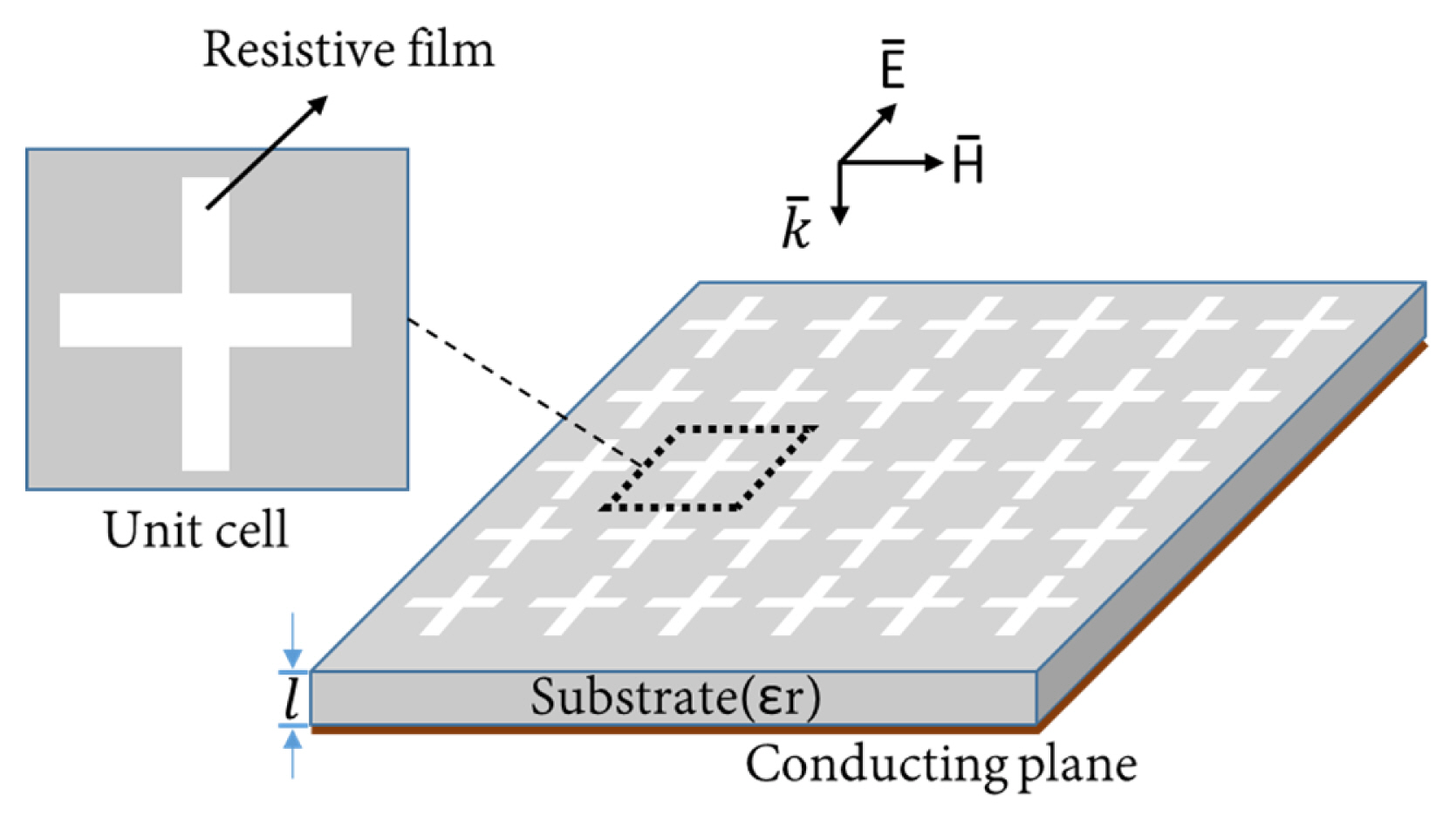
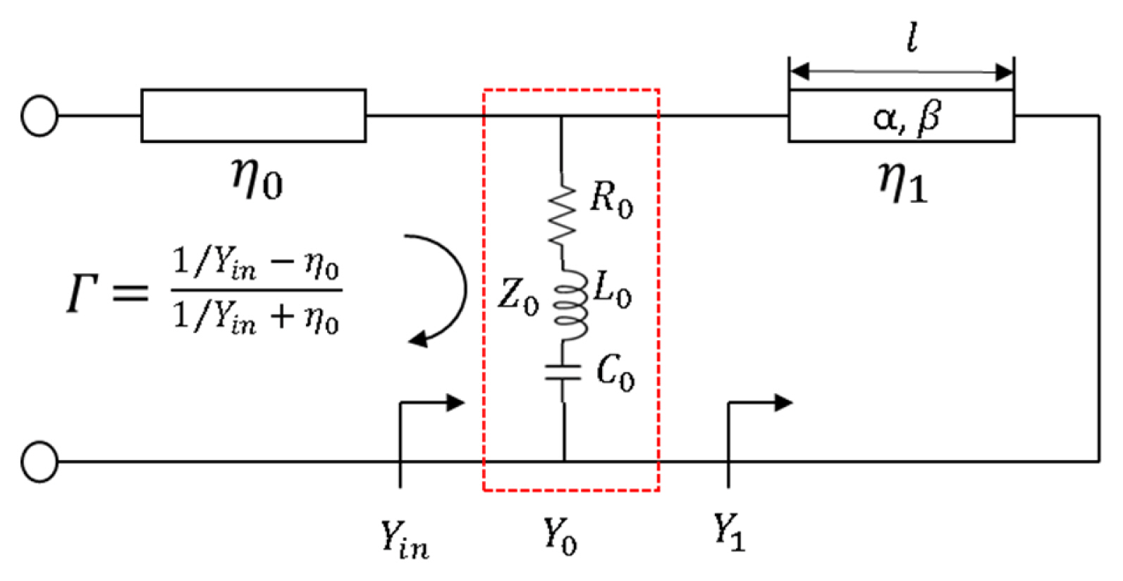
Fig. 1 shows the geometry of a single-layer microwave absorber using a reactive RLC screen, which is realized by a periodic cross-dipole structure placed above a conducting plane. The permittivity of the substrate is ╔ør. A simple dipole-type structure on a AgNW resistive film is used as a reactive screen. Fig. 2 is the equivalent circuit of Fig. 1 when the EM wave is normally incident. The dipole-shaped structure is modelled as a lumped series RLC resonator characterized by of R0, L0, and C0. In the equivalent circuit, ╬Ę0 (= 377 ╬®) and ╬Ę1 are the intrinsic impedances of free space and the substrate, respectively. Z0 is the impedance of the RLC reactive screen alone. Y1 is the input admittance at the input terminal of the shorted transmission line with length l. The characteristic impedance of the transmission line is ╬Ę1. ╬▒ is the attenuation constant, and ╬▓ is the propagation constant. Yin is the total input admittance of the RLC screen. If the electrical length ╬▓l at a design angular frequency Žē0 and intrinsic impedance ╬Ę1, with the permittivity of the substrate are specified, the RLC values (R0, L0, and C0) can be determined and used to obtain the dimensions of the dipole structure through EM simulations, as shown in Section III.
In Fig. 2, the admittance Y0 of the RLC screen is
The input admittance Y1 of the shorted transmission line is
where l is the physical length, and ╬│ = ╬▒ + j╬▓ is a complex propagation constant of a lossy line. The attenuation constant ╬▒ can be written in terms of loss tangent (tan╬┤). ╬▒l is given by
and ╬▓l is given by
╬▓ l = ╬Ė 0 Žē Žē 0
The input admittance Yin as a function of frequency is given by
(4)
The reflection coefficient ╬ō and the absorption A are given by
and
The condition of perfect absorption (A = 1) at Žē0 is that Eq. (5) is zero at Žē0. This condition results in
(7)
and
(8)
One more chosen condition to uniquely determine R0, L0, and C0 is that the slope of the imaginary part (Bin) of input admittance (4) should be 0 at Žē = Žē0 [24], given by
If the differentiation of Bin is 0 (9) and satisfies (7) and (8) at Žē0, it is guaranteed that the absorption is perfect at Žē0 and has the widest bandwidth possible. Note that the real part (Gin) of input admittance (4) is flatter than Bin near Žē0, especially when ╬Ė0 approaches 90┬░. Eq. (9) is expressed as follows:
(10)
where
(11)
and
(12)
Eqs. (7), (8), and (10) are simultaneously solved for R0, L0, and C0. The resistance R0 in Fig. 2 is given by
(13)
The inductance L0 and capacitance C0 can be obtained from the two equations as follows:
(14)
and
(15)
and
The closed-form solutions for R0, L0, and C0 are all related to the intrinsic impedance (╬Ę1), loss tangent (tan╬┤), and electrical thickness (╬Ė0) (at Žē0) of the substrate.
2. Verification of Closed-Form Solutions
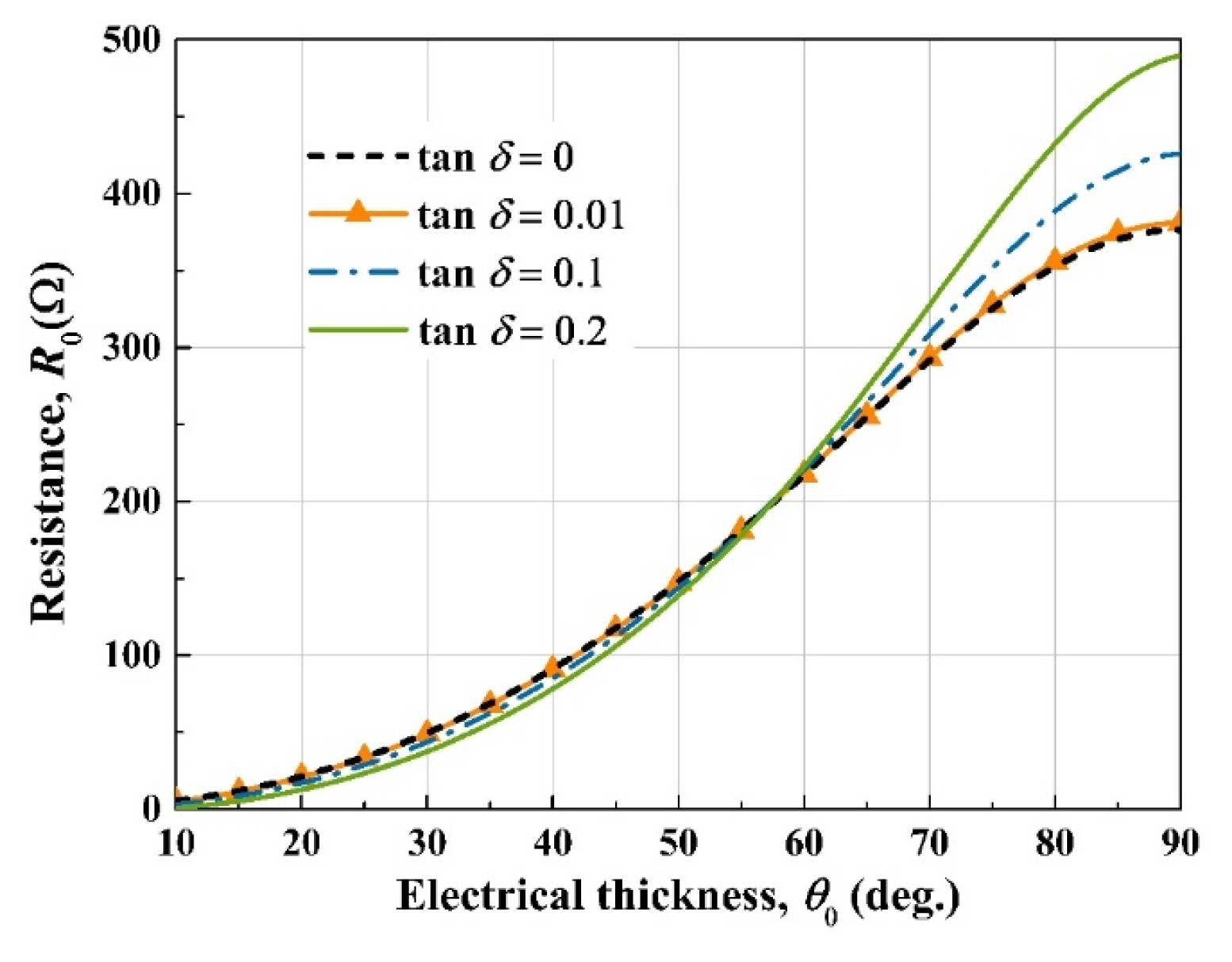
The values of R0 (13) with different electrical thicknesses and loss tangents are shown in Fig. 3. As the electrical thickness ╬Ė0 becomes larger, the value of R0 also becomes larger. When the loss tangent is smaller than 0.01, the value of R0 is almost the same as in the case of no loss. The effects of loss on the substrate are shown to be more pronounced when ╬Ė0 is greater than 70┬░. Note that, when the loss tangent is zero and ╬Ė0 is 90┬░, R0 approaches 377 ╬® which is same as SalisburyŌĆÖs. The values of L0 (16) and C0 (17) with different electrical thicknesses and loss tangents are plotted in Fig. 4. The effect of the loss tangent is not significant in C0 but is relatively more significant in L0, especially when ╬Ė0 is greater than 70┬░.
When the loss tangent of the substrate is assumed to be zero, solutions (13) and (16)ŌĆō(17) are simplified to
and
Especially when ╬Ė0 is 90┬░, the above solutions are simplified again to those in [5]. Thus, we can see that the solutions presented in this work are general and can be applied to any thickness, permittivity, loss tangent of the substrate, and frequency.
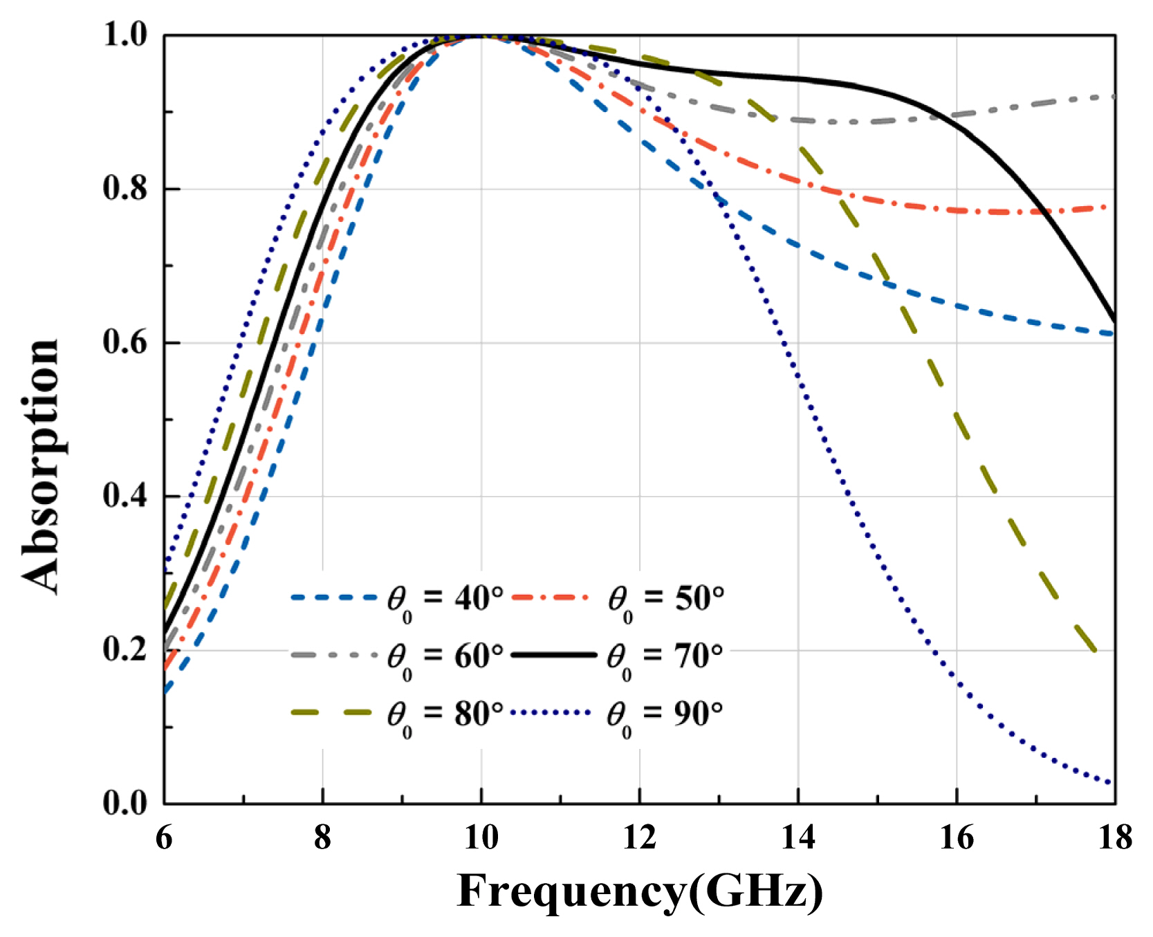
Fig. 5 shows the absorption (6) for different electrical thicknesses of the absorber. The widest bandwidth is obtained when ╬Ė0 is 70┬░. The 90% (A = 0.9) bandwidth is approximately 8 GHz, from 8.2 GHz to 16.2 GHz (66% at a center frequency of 12.2 GHz or 80% at a design frequency of 10 GHz).
Based on these observations, the specifications of the desired absorber are summarized in Table 1. The design frequency is 10 GHz for X-band absorber applications. The relative permittivity and loss tangent of the substrate are 2.2 and 0.001, respectively. The obtained values of R0, L0, and C0 using (13) and (16)ŌĆō(17) are shown in Table 2.
III. Fabrication and Measurement
The absorber with crossed-dipole patterns (Fig. 1) based on the parameters shown in Tables 1 and 2 is realized using an EM simulator (High Frequency Simulation Software), fabricated, and measured. The reason why the crossed-dipole pattern is chosen among other structures is that it is the simplest and easiest to implement. Moreover, its absorption characteristics are almost independent of the polarization of incident waves, as will be shown later.
1. Design and Simulation
Fig. 6 shows the geometry of the absorber unit cell. a is the side length of the square absorber unit, and w and h are the width and height, respectively, of the crossed-dipole pattern on a resistive film. Rs is the resistance per square of the film material, and g is the gap distance. To realize the real part (R0 = 291.86 ╬®) of the reactive screen, a AgNW film with 23 ╬®/square is used. AgNWs are chosen for fabrication because the sheet resistance of the film can be easily controlled by adjusting the concentration of the AgNW solution. The width (w) and length (h) of the dipole structure affect the resistance R0, which is given by Rsh/w, where Rs is the surface resistance of the resistive sheet (╬®/square). By choosing Rs and the aspect ratio h/w properly, a specifically required R0 can be realized in many ways. Moreover, L0 and C0 are proportional to h/w and w/g, respectively. By using these characteristics, the overall dimensions of the crossed-dipole structure can be determined using an EM simulator.
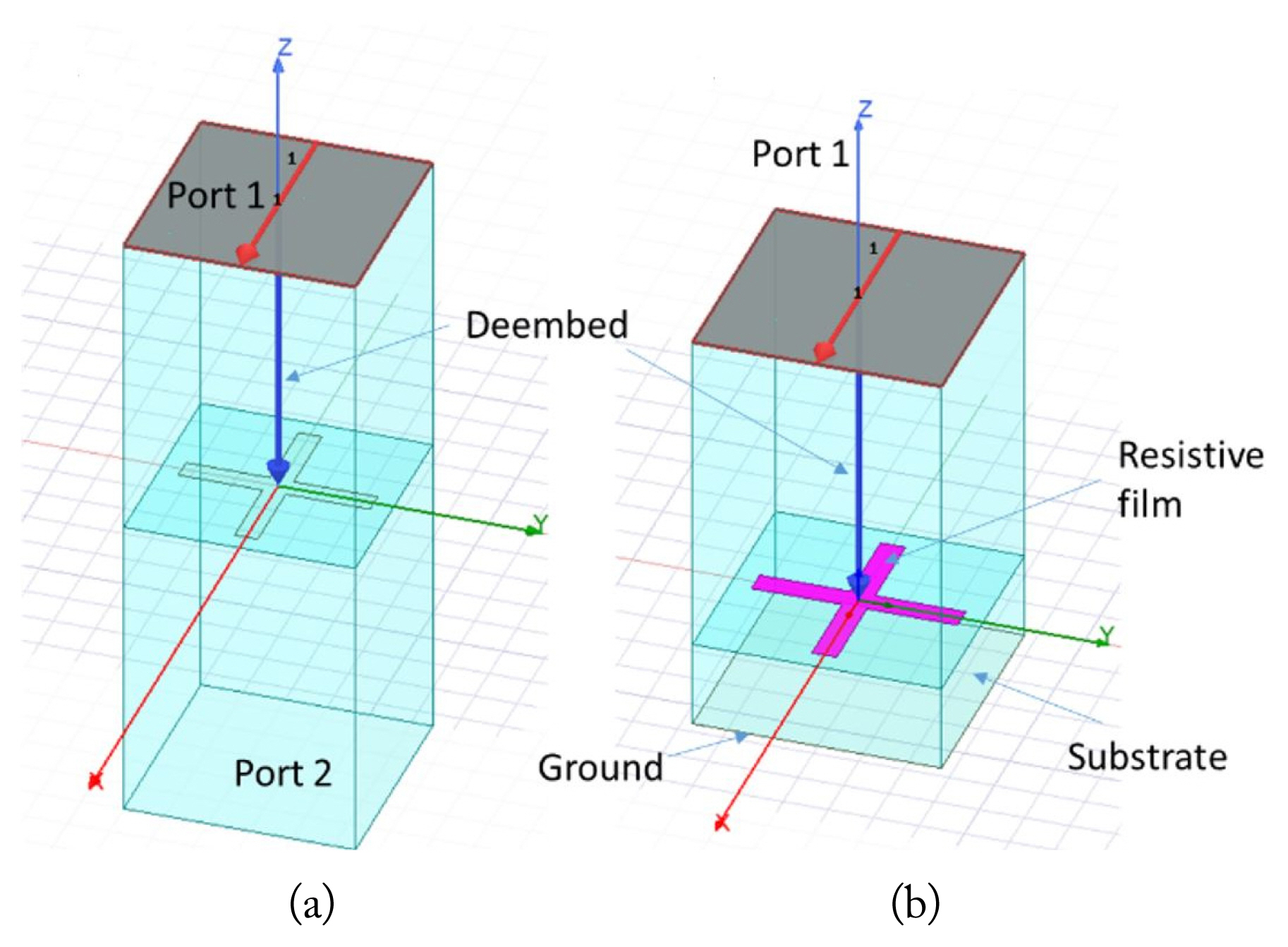
The first step is to determine the dimensions of the crossed-dipole in which the circuit values in Table 2 are realized. To evaluate the impedance of only the reactive screen in HFSS, deembedding from the ports to the reactive screen is performed, as shown in Fig. 7(a). After the realization of the structure on the reactive screen, the substrate and ground are added below the reactive screen, as shown in Fig. 7(b). The final dimensions of the absorber are listed in Table 3.
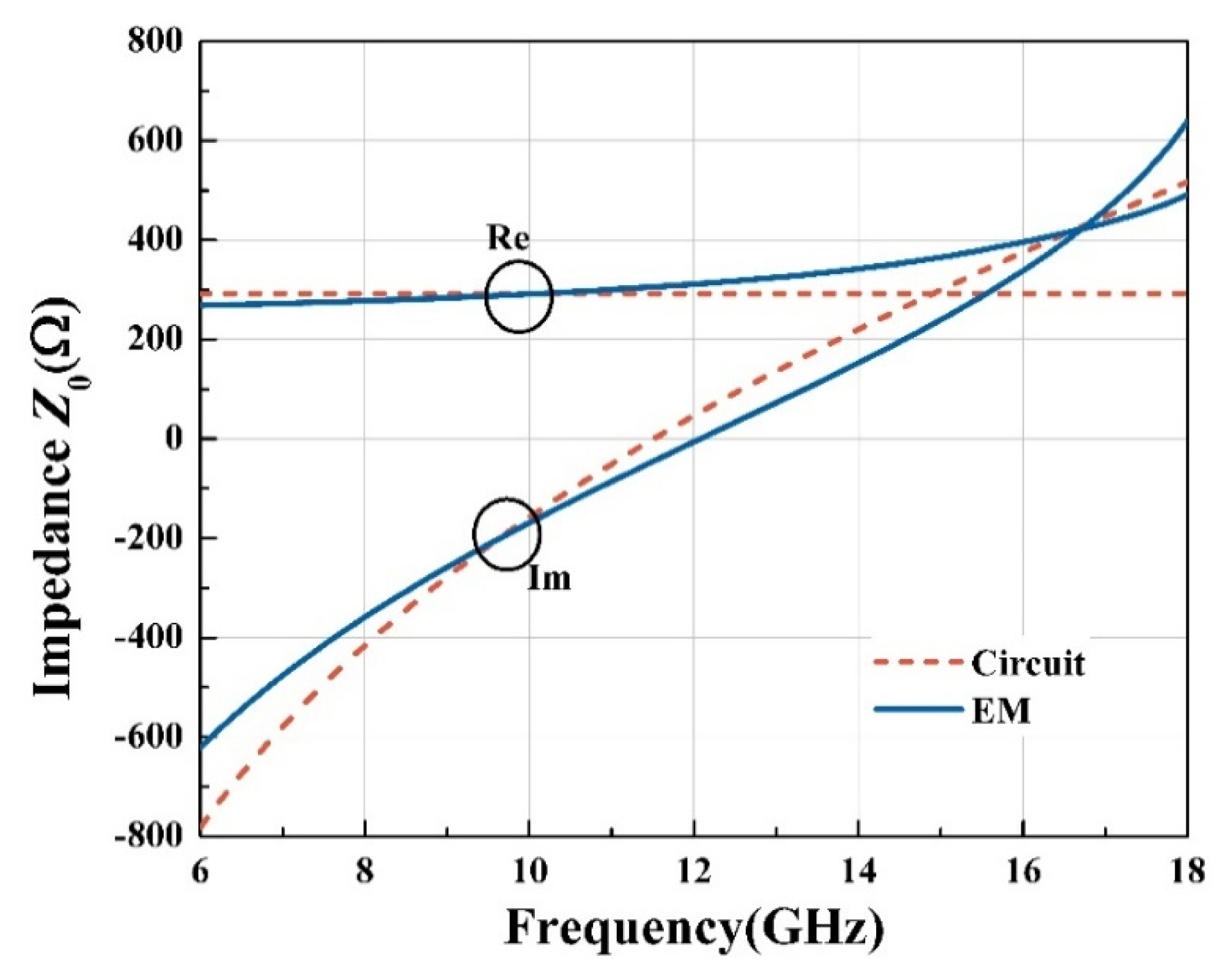
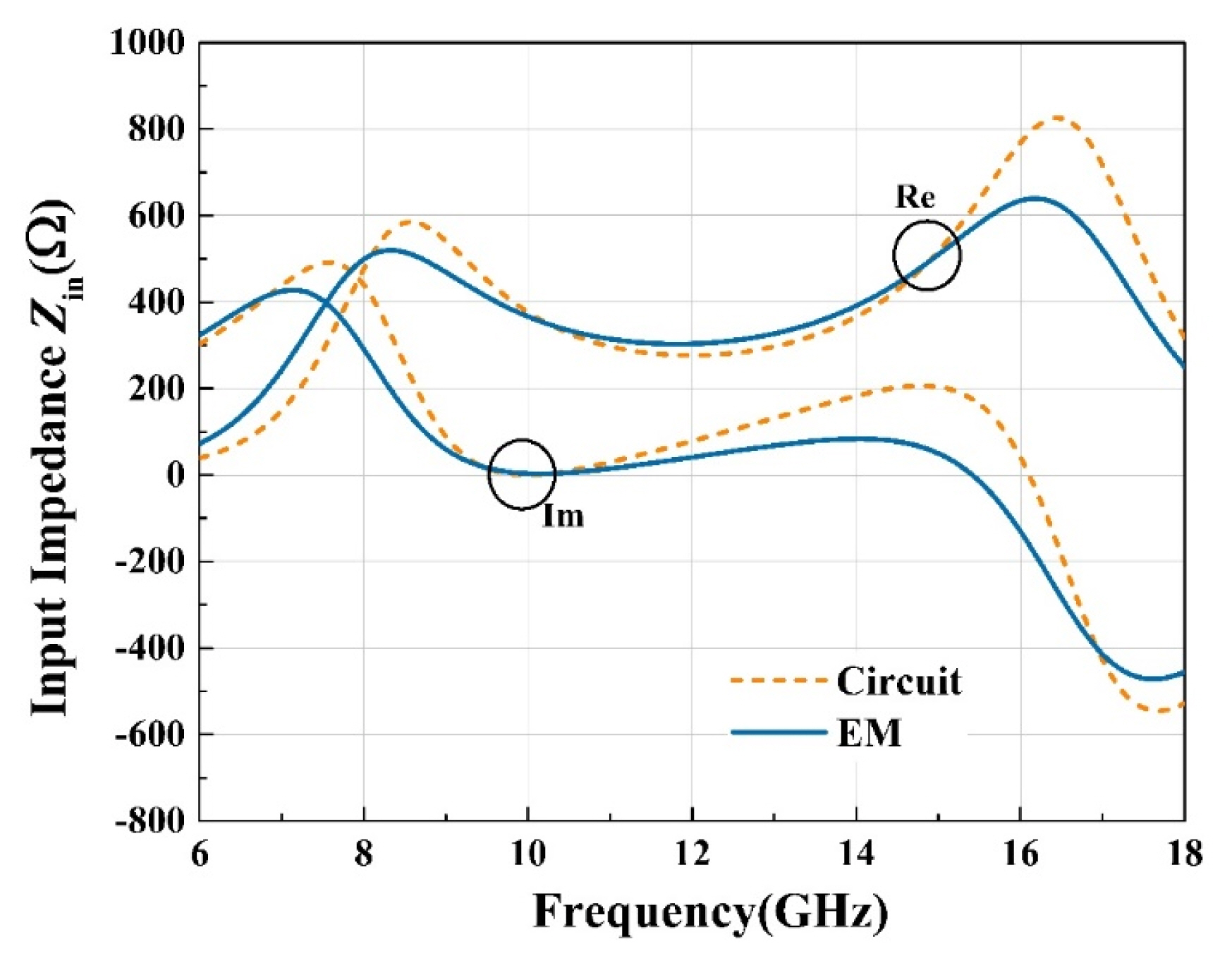
Fig. 8 shows the resistance and reactance of the impedance only for the reactive RLC screen based on circuit and EM simulations. The circuit simulation results are used as a reference in determining the dimensions of the crossed-dipole structure. Even though the lumped circuit values in Table 2 are used in the circuit simulation, and the crossed-dipole in the unit cell size of 0.37╬╗0 is not smaller than the wavelength, a good resemblance between them is observed. The input impedance Zin, as defined in Fig. 2 and simulated based on Fig. 7(b), is shown in Fig. 9 as a function of the frequency based on the EM and circuit simulations. Without any adjustment to the designed crossed-dipole structure, the EM simulation results reasonably agree with the circuit simulation results. The circuit modelling of the crossed-dipole structure (0.37╬╗0 in Table 3) by the lumped elements R0, L0, and C0 is expected to intrinsically lead to some discrepancies between the circuit and EM simulations. Despite these discrepancies, the design guidance by circuit modelling is helpful. Note that the imaginary part is zero (resonant) with a flat slope, and the real part is 377 ╬®. This enables perfect absorption (or match) at the design frequency and maximum bandwidth.
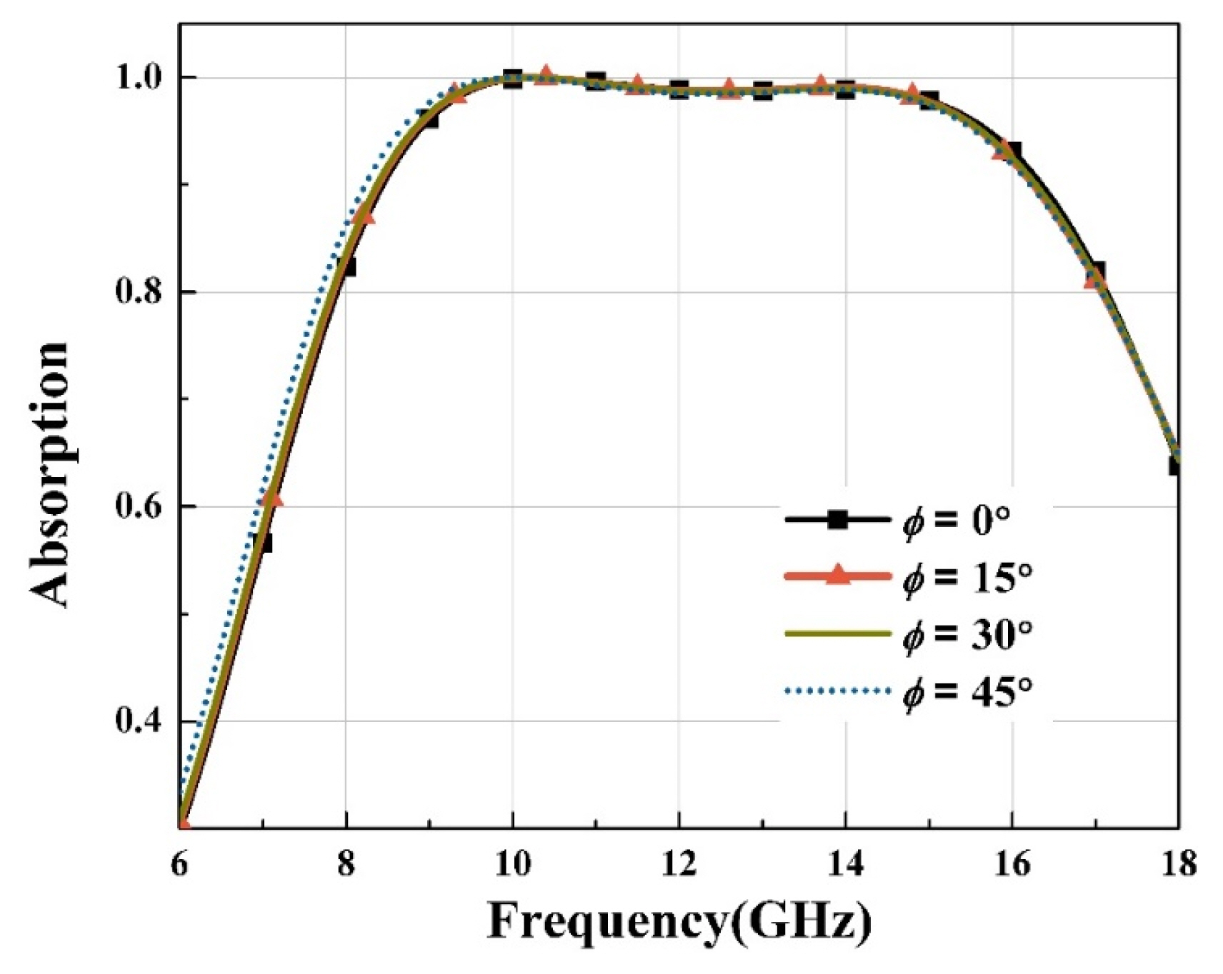
Fig. 10 shows the EM-simulated absorptions depending on the polarization angles (Žå) of 0┬░ŌĆō45┬░. The absorption is almost independent of the polarization angle because of the crossed-dipole structure employed. The degradation effects of microwave absorbers with oblique TE and TM incidence cases are mostly similar to those in [7].
2. Fabrication and Measurement
Fig. 11(a) is a photograph of the fabricated absorber made of a AgNW resistive film, a substrate, and a conducting plane. The absorber consists of 25 ├Ś 17 unit cells, and the overall size is 270.5 mm ├Ś 183.9 mm ├Ś 4.5 mm. The experimental setup is illustrated in Fig. 11(b). Absorption was measured using a high-gain horn antenna of Model BBHA9120D (1ŌĆō18 GHz; Schwarzbeck, Sch├Čnau, Germany). Fig. 12 shows the measured absorption compared with the circuit and EM simulation results. The measured absorption in Fig. 12 was obtained based on a special calibration for the network analyzer and with the use of a conducting plane at the back of the absorber as a reference [6]. The distance between the horn antenna and the absorber is 5╬╗0 (15 cm) at 10 GHz. The 3 dB beamwidth (in the E and H planes) of the horn antenna is approximately 45┬░ at 10 GHz. Some variations of this distance (5╬╗0) do not affect the measured reflection coefficient and absorption at the absorber. The absorption results are shown to reasonably agree with each other. Some differences between the simulations and the measurement could have resulted from the non-uniformity of the resistivity in the AgNW film and the limited size of the absorber in the measurement. According to the specification, the surface resistance of the AgNW resistive film (Kolon Industries, Seoul, Korea) is 23 ╬®/square ┬▒4%.
IV. Conclusion
Closed-form solutions for the design of thin and wideband microwave absorbers have been derived and presented based on an equivalent circuit. These solutions can be used for any design frequency, substrate thickness, and permittivity/loss tangent. As a design example, a microwave absorber with a design center frequency of 10 GHz with 70┬░ electrical thickness has been designed using the derived solutions and fabricated using a AgNW resistive film with a surface resistance of 23 ╬®/square. The measured absorption shows consistent results with the circuit (theory) and EM simulations, validating the effectiveness of the proposed design procedures. A thin and wideband absorber can now be more easily designed without unnecessary trial-and-error efforts or complicated processes.