I. Introduction
Dielectric properties (e.g., permittivity) of chemical and bio-molecules is useful for a variety of applications. In agriculture, the quality of its products is improved by measuring the permittivity of soil and leaves [1, 2]. For example, crop quality control is usually carried out by regularly monitoring the water content of crops [1]. The dielectric characterization is also employed in biomedical sensors, such as the monitoring of blood glucose and semen activity [3ŌĆō6].
In [7], a complementary metal oxide semiconductor (CMOS) based transceiver IC is presented as a dielectric spectroscopy device, but an off-chip sensing capacitor is utilized to measure the off-chip liquid material under test (MUT). This off-chip sensing capacitor is implemented on the printed circuit board (PCB) with a bulky footprint and accompanying parasitics degrading the measurement accuracy. In [8], a PCB-integrated microwave sensor for the dielectric measurement of liquids is presented. The resonant frequency and the Q factor of the off-chip microwave sensor are used to estimate the complex permittivity of the material to be tested. However, the work in [8] also suffers from a large area, and additional packaging processes increase the cost of the permittivity sensor. Thus, integrated sensors on silicon to detect the permittivity of chemical and biochemical are promising with a reduction in its size and cost while offering lower power consumption [9].
Capacitance can be determined if the geometry of the conductor and the dielectric properties of the insulator between the conductors are given [10]. Then, dielectric spectroscopy is accomplished by measuring the admittance (or impedance) of the sensing capacitor whose dielectric constant is dictated by the MUT and extract its dielectric constant from the material dependent capacitance.
A sensing capacitor, as a critical interface between the MUT and the spectroscopy measurement system can be implemented in either on-chip or off-chip [7ŌĆō9, 11]. As mentioned earlier, an off-chip sensing capacitor suffers from large parasitics and its bulky size. The interconnection between an off-chip capacitor and a spectroscopy device requires a careful attention as well.
In this work, we propose a design and am implementation of an on-chip capacitor for dielectric constant extraction featuring a small sensor size and lower parasitic, and built a low-cost. Utilizing the top metal in the CMOS back-end, inter-digitized conductors are fabricated using 28-nm CMOS technology. The dielectric properties between inter-digitized conductors are governed by the off-chip liquid MUTs by opening the passivation layer. The permittivity of the MUT is extracted within the 100 MHzŌĆō5 GHz frequency range by measuring the forward voltage-gain (S21). Permittivity as a function of |S21| at each frequency can be extracted by polynomial curve fitting. Additionally, we propose the weighted |S21| equation to improve a sensor accuracy. Through a proposed curve-fitting calibration method, less than 6.4% root-mean-square (rms) error is successfully achieved when propanol (C3H8O) is used as a material.
This article is organized as follows. Section II discusses a simple but intuitive circuit model for the sensing capacitor. Section III presents measurement results and polynomial curve fitting method for calibration. The conclusion of this article is in Section IV.
II. Circuit Model of Sensing Capacitor
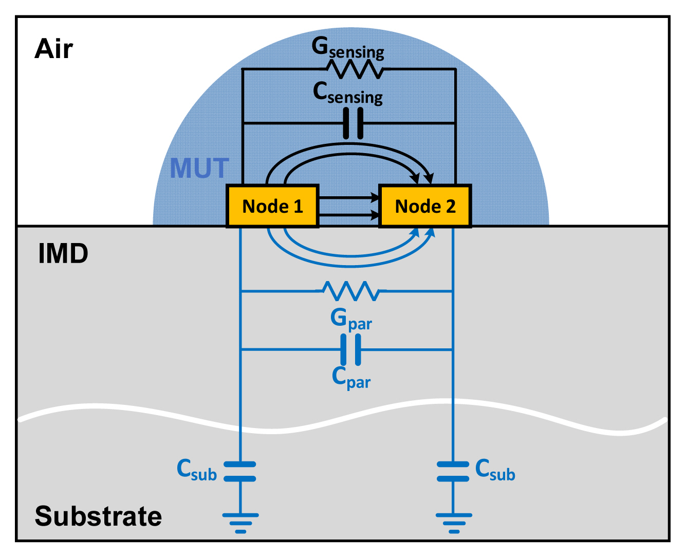
Fig. 1 shows the illustration of an on-chip sensing capacitor whose dielectric property is governed by the MUT. The sensing capacitor is in an inter-digitized fashion implemented with the top metal of the CMOS back-end process (LB in the 28-nm Samsung CMOS process). The passivation layer has to be removed in order to contact the top metal directly to MUT.
A side section view of the on-chip sensing capacitor with a simple equivalent circuit model is depicted in Fig. 2. Capacitance and conductance denoted as Csensing and Gsensing are due to the E-fields passing through the MUT by two inter-digitized top metal nodes, while the E-fields passing through the inter-metal-dielectric (IMD) create undesired parasitic capacitance and conductance modeled as Cpar and Gpar, which are not related to the characteristics of the MUT. Additionally, capacitance due to the substrate, Csub, is part of the network, which degrades the accuracy of the permittivity detection.
In the case of Csensing and Gsensing, their values are determined according to the permittivity of the MUT (╔øMUT = ╔øMUTŌĆ▓ ŌĆō j ┬Ę ╔øMUTŌĆ│). In contrast, Cpar and Gpar are fixed values governed by permittivity of the IMD (╔øIMD = ╔øIMDŌĆ▓ ŌĆō j ┬Ę ╔øIMDŌĆ│).
Excluding the effect of Csub, the real-part of admittance between two inter-digitized electrodes (Ys) comes from Gsensing and Gpar, while the imaginary part of Ys is composed of Csensing and Cpar. Gsensing and Gpar are circuit components due to the imaginary permittivity of MUT ╔øMUTŌĆ│ and IMD ╔øIMDŌĆ│, respectively, which corresponds to an energy loss. Csensing and Cpar come from the real permittivity of MUT ╔øMUTŌĆ▓ and IMD ╔øIMDŌĆ▓, respectively, representing energy storage [12]. Combined admittance between two electrodes can be expressed as follows.
(1)
where C0 (C1) are coefficients of effective capacitance due to MUT and IMD and f(┬Ę) and g(┬Ę) denote nonlinear mapping functions from the permittivity of MUT to admittance as a result.
To improve the sensitivity in measuring the permittivity of MUT, parasitic capacitances, Cpar and Csub in parallel with the desired capacitance, Csensing, have to be minimized. Csub can be made small by narrowing the spacing of the two nodes of the sensing capacitor. At the same time, narrow spacing between two electrodes reduces the self-resonant frequency (SRF) as a result of an increase in Csensing and mutual inductances. The inductances caused by the geometry of the on-chip sensing capacitor have a direct trade-offs with the size of the sensing capacitor such as a spacing and the width of the top metal. Thus, in this work, the target frequency band and area of the chip are budgeted in advance, and the optimal sensing capacitor dimension is determined in consideration of the above mentioned trade-offs.
The top metal is composed of aluminum, and an oxide layer is created when the top metal is exposed to the MUT without any passivation (protection). The thick oxide film attenuates the electric field and reduces the sensitivity of the sensing capacitor. In the fabricated chip, the oxide film thickness ranges from 1 to 5 nm [13]. The electromagnetic simulation was performed and the sensitivity was not degraded even with 10 nm oxide film thickness. This thin oxide film, on the other hand, is beneficial by protecting the sensing capacitor from the damage and chemical reaction due to its high corrosion resistance and wear resistance.
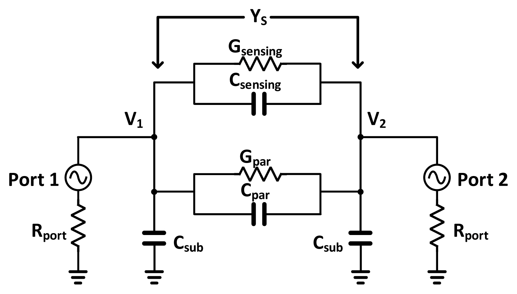
Fig. 3 shows the schematic model of the sensing area with a two-port vector network analyzer (VNA). The forward voltage gain (S21) of this network can be calculated by finding the ratio between the injected voltage source (V1) and the load voltage (V2) while, the network is terminated with the port load impedance (Rport).
(2)
In both the numerator and the denominator, the resistance (Žē ┬Ę g(╔øMUTŌĆ│ )) due to the imaginary part of permittivity is significantly smaller than those of the other components. For instance, long transmission lines, connected in series with a sensing capacitor, makes Ys more capacitive. Thus, we can simplify Eq. (2) into the following formula:
The dominant pole is calculated to be
Žē p = 1 R p o r t ┬Ę ( f ( ╔ø M U T ŌĆ▓ ) + C s u b )
III. Measurement Results and Curve Fitting Calibration
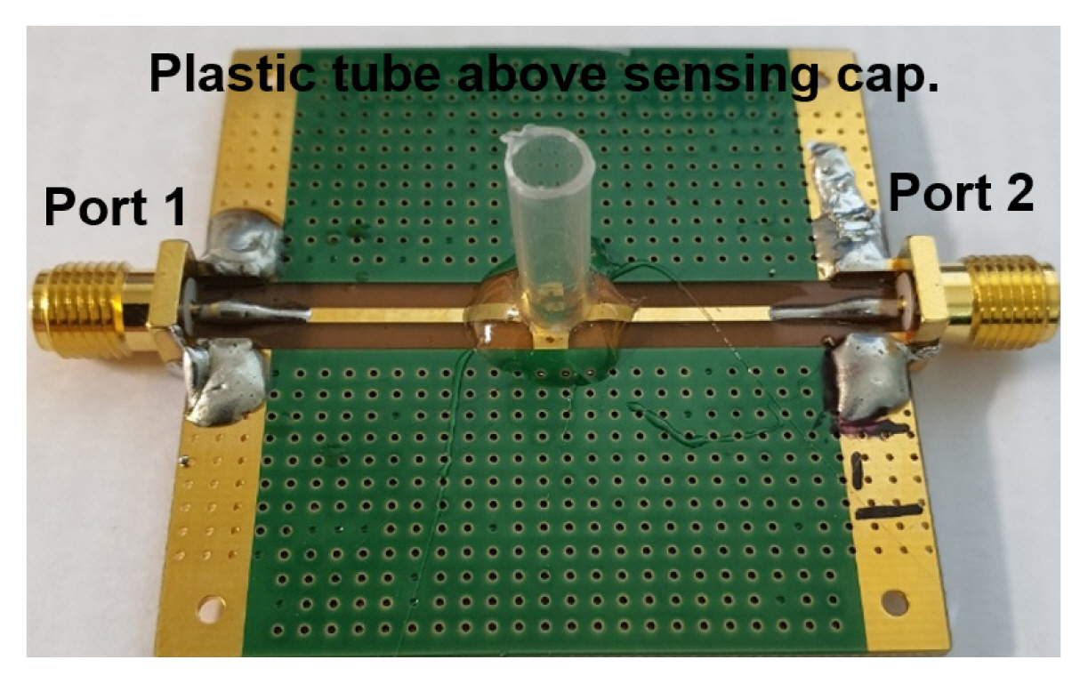
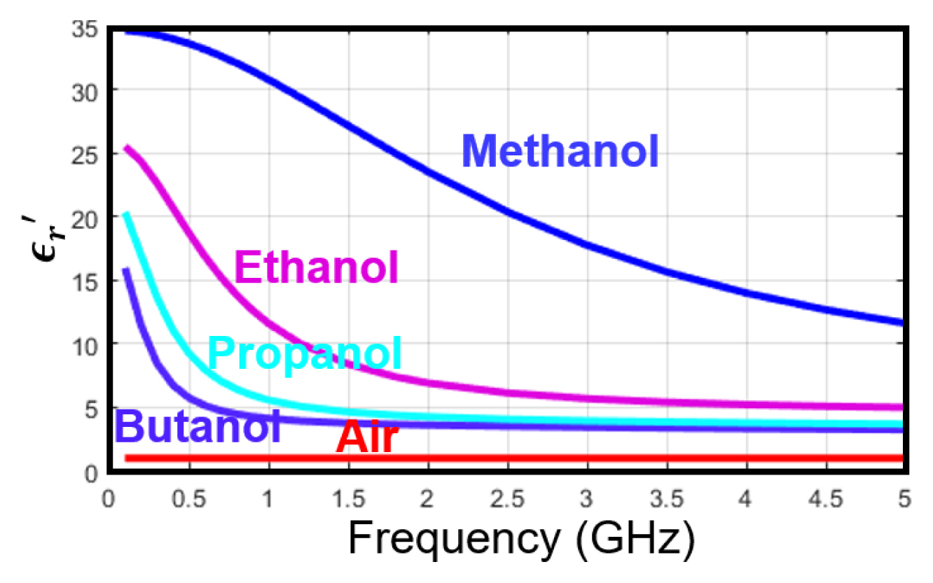
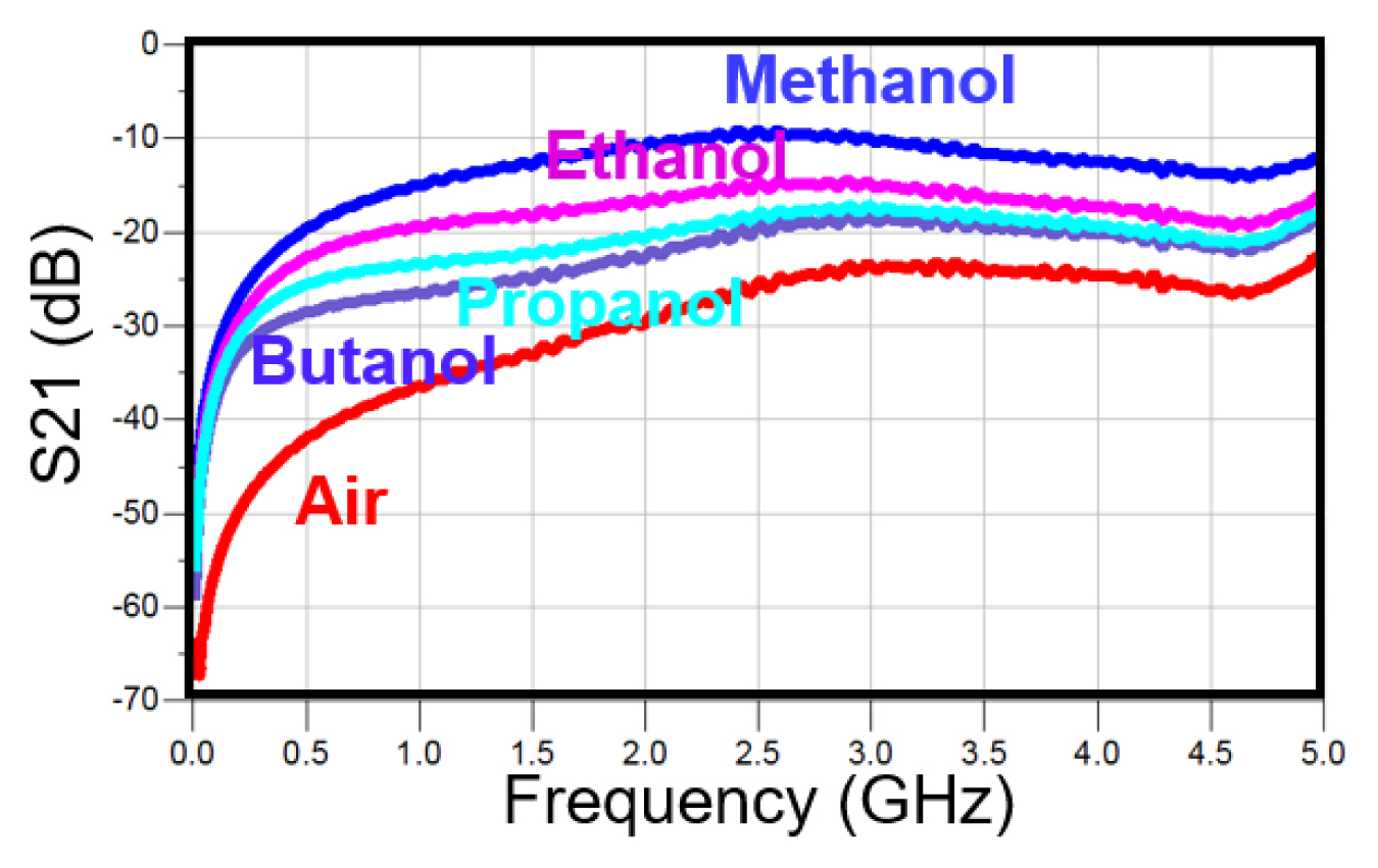
For the measurement of scattering parameters of the fabricated sensor, PCB consisting of the mounted chip, interconnect transmission lines, and input/output ports are assembled as shown in Fig. 4. During the chip packaging process, the insulating epoxy was covered except for the fabricated capacitor area. With a plastic tube on top of the chip, the MUTs were injected through the micropipette (Eppendorf Research plus 3120000038). Fig. 5 shows the real part of the permittivity (╔øŌĆ▓) for methanol, ethanol, propanol, butanol and air over the frequency range of 0.1ŌĆō5 GHz [14]. The measured forward voltage gain (S21) at room temperature is given in Fig. 6, which shows that the magnitude of S21 is proportional to ╔øŌĆ▓ over the measured frequency range.
To extract ╔øŌĆ▓ of the MUT from the measured S21 data, the curve-fitting calibration is performed first. Methanol, ethanol, butanol, and air are selected as reference materials, where the information on their real permittivity is provided in [14]. The real permittivity is then curve-fitted at each measured frequency by third order polynomial function with the measured |S21|.
The detailed polynomial curve fitting procedure from the measured |S21| is elaborated below:
1. For each frequency, f1, to be curve fitted, reference materials are injected into the sensing capacitor and its |S21| is measured through a VNA.
-
2. The ╔øŌĆ▓ of the reference materials are least-square fitted to third order polynomial function with respect to the measured |S21|.
3. The fitting parameters ╬▒0, ╬▒1, ╬▒2, and ╬▒3 can be found and saved by using the least-square fitting method to fit the polynomial regression function. This procedure is repeated over the entire measurement frequency.
Once the curve-fitting procedure is finished, the unknown permittivity of MUT can be calculated by utilizing its measured |S21| along with the calculated fitting parameters.
Given the above procedure, the permittivity of any unknown MUT can be extracted. To further enhance the measurement accuracy, we propose reshaping (weighting) the parameter, given the measured S21. Instead of utilizing raw |S21|, we give the weights ╬▓ on the imaginary part of S21 and (1ŌĆō╬▓) on the real part of S21. The weighting function can emphasize/deemphasize the relevant terms to minimize the extraction error. The revised magnitude of S21 is given by
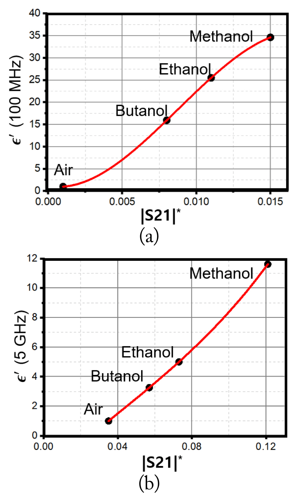
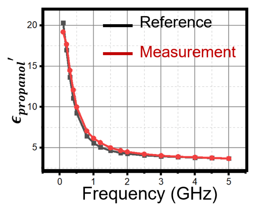
Fig. 7 shows the curve-fitted polynomial function and the real permittivity of the reference materials at 100 MHz and 5 GHz frequency with the frequency-dependent parameter ╬▓. From the extracted curve-fitted polynomial function, the permittivity of propanol is found to have a good correlation with reference value as shown in Fig. 8. By replacing |S21| with the proposed equation, the rms permittivity error of measurement is lowered from 9.1% to 6.4% over the frequency range of 0.1ŌĆō5 GHz.
The proposed spectroscopy sensor is compared to the reported research works as depicted in Table 1. Our work is realized in a compact footprint (0.03 mm2) on chip, while the operating frequency range is the second largest.
More reference materials for calibration can be added to minimize the permittivity error (higher polynomial function). The off-chip and on-chip transmission line in series with the sensing capacitor complicate the mapping function and degrade the accuracy accordingly. Their length then needs to be minimized to further enhance the measurement accuracy.
IV. Conclusion
An on-chip capacitive sensor for dielectric spectroscopy is implemented in this work. Based on the circuit model of the on-chip sensing capacitor, the permittivity extraction method is proposed and the measurement result verifies the successful detection of the real part of the permittivity in the frequency range of 0.1ŌĆō5 GHz. The inter-digitized sensing capacitor can be optimized in its sensitivity and SRF in consideration of the fabrication trade-offs. To improve the permittivity detection accuracy, the measured forward voltage-gain is curve-fitted by the polynomial regression function. The revised forward voltage-gain parameter is suggested for the detection and the measured permittivity of the propanol shows 6.4% rms error compared with the theoretical value.