I. Introduction
The use of flexible printed circuit boards (FPCBs) in electronic devices has been increasing as these devices become thinner and smaller. Meshed ground planes have been adopted in FPCBs for impedance matching and improved flexibility [1–8]. Apertures of meshed ground planes cause an effective dielectric constant change and a roundabout current path that increase the inductance of the ground plane [9]. Two identical traces of a differential pair would have asymmetric return current paths on a meshed ground. This imbalance would result in mode conversion, intra-pair and inter-pair skews, increased radiated emissions, and characteristic impedance variation [10–13].
To mitigate this, Hsu et al. [14] proposed the use of co-planar waveguides with a ground by adding a guard traces on both sides of the transmission line to mitigate the asymmetry in the microstrip line with a meshed ground. The guard traces replace the asymmetric return current paths in the mesh ground plane. However, the guard traces take up space that is already lacking. Wang et al. [15] proposed rotating a meshed ground by 30° rather than the conventional 45° relative to differential traces. While the impedance variation was reduced, the mode conversion did not significantly improve. Moreover, in silicon interposer, which has been actively studied recently, various design parameters in a meshed ground for impedance matching have been studied, but no new structure has been proposed [16, 17]. We introduced an offset mesh structure to alleviate the impedance variation of single-ended lines [18]. This offset mesh structure uses only the conventional top and bottom meshed ground, without additional guard traces. Therefore, this structure mitigates the imbalance that differential pairs would have without taking up additional space.
In this study, we applied the offset mesh structure to a differential pair to minimize the imbalance of the pair. There were aperture regions and a solid region with a lattice pattern in the meshed ground. Apertures of the mesh ground plane caused asymmetry. The differential pair passed the aperture region at both the top and bottom simultaneously, as shown in Fig. 1(a) and 1(b), which worsened the asymmetry between two identical traces of the differential pair. Our approach was to offset the centers of the meshes on the two layers. If a routed trace landed on top of an aperture on the top layer, it should land on a solid part of the bottom layer (or vice versa). The validity of this approach was confirmed with the results of a full 3D electromagnetic (EM) solver, the ANSYS High-Frequency Structural Simulator (HFSS) [19], CST Microwave Studio [20], circuit simulations, and Advanced Design System (ADS) software [21].
II. Configuration of the Offset Mesh
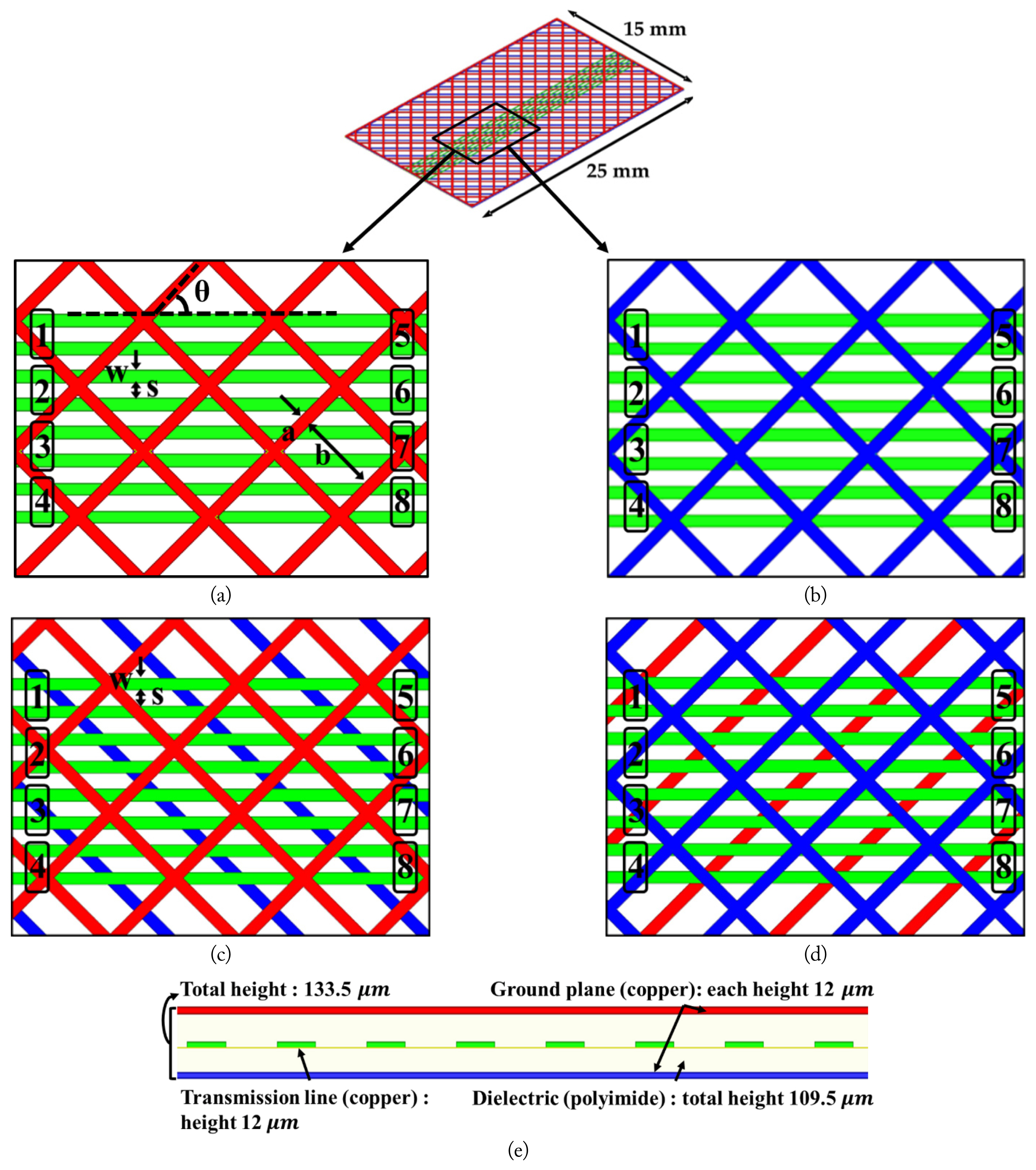
The geometry of the proposed offset mesh structure is shown in Fig. 1. The meshed ground consists of aperture regions and a solid region with a lattice pattern. Four differential pairs of eight striplines run parallel to one another between two meshed grounds. The configuration of the conventional mesh is the stripline structure with a meshed ground in Fig. 1(a) and 1(b). The configuration of the offset mesh offsets the centers of the meshes on the two layers in Fig. 1(c) and 1(d). In this way, if a routed trace lands on a solid region of the top layer, it should land on top of an aperture region on the bottom layer (or vice versa). There are mainly three variables in designing a mesh plane: (1) a trace-to-aperture intersecting angle, (2) the ratio of the aperture to the solid region, and (3) the position of the trace on the meshed plane [6].
We compared the proposed offset mesh and the conventional mesh by fixing the first two design variables. The trace-to-aperture intersecting angle of both variables, θ, was set at 45°; the size of a square aperture, b, at 1,000 μm; the edge-to-edge distance of adjacent apertures (separation), a, at 150 μm; the trace width, w, at 150 μm; the trace length, l, at 25 mm; and the trace spacing, s, at 200 μm. Eight differential ports were assigned as shown in Fig. 1, and the differential pairs 1–4 represented port 1–5, port 2–6, port 3–7, and port 4–8, respectively.
III. Results
1. Differential Insertion Loss and Characteristic Impedance Variation
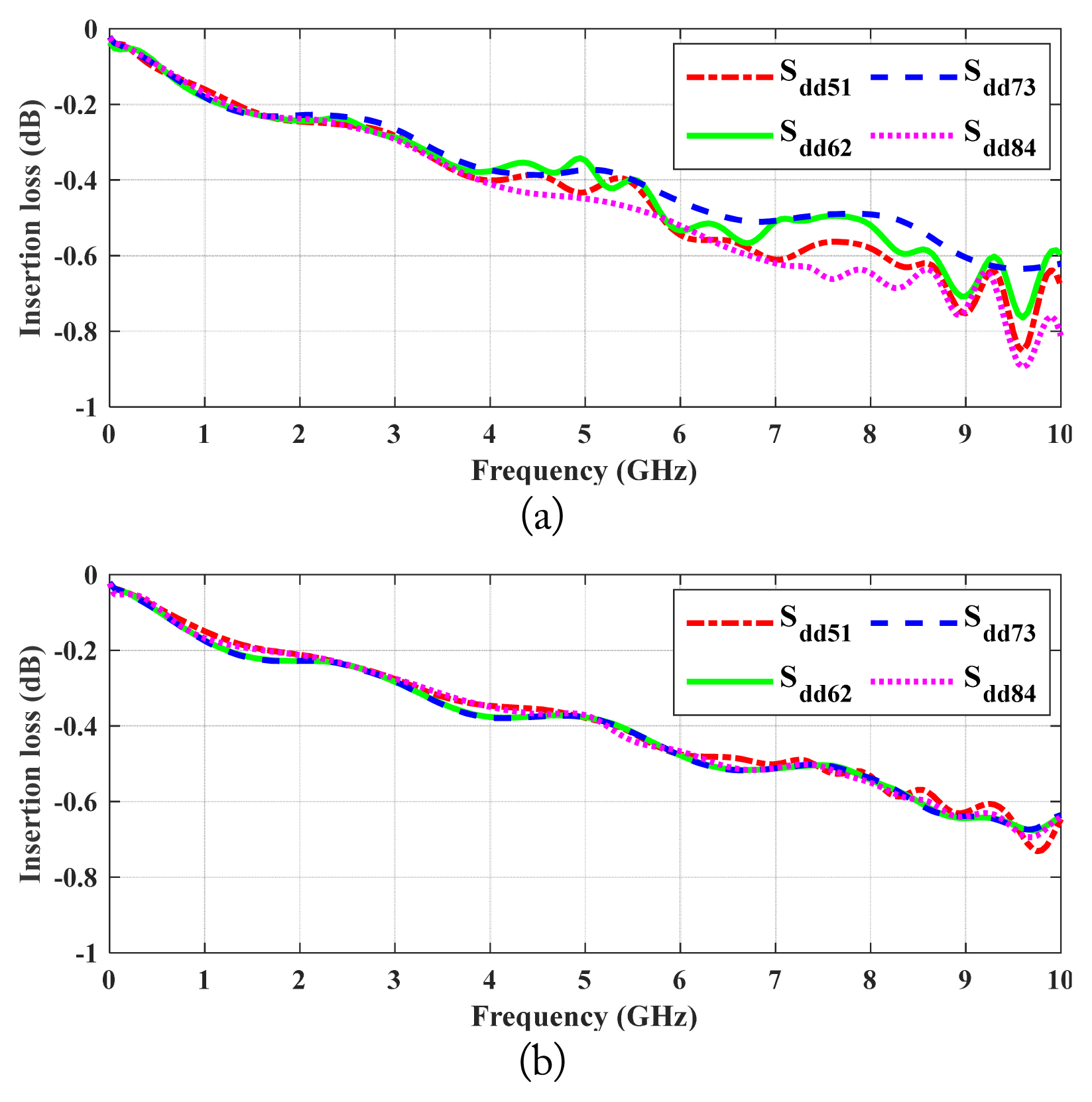
To analyze the signal integrity of the differential pair, the differential-to-differential mixed-mode S-parameters, Sdd [22], were used to verify the simulation results. Fig. 2 compares the insertion loss of the differential pair on the conventional mesh with that on the offset mesh. The latter performed at least as well as the former. Moreover, the latter showed less variation in the insertion loss than the former depending on its position.
The characteristic impedance of a single-ended trace is significantly affected by the position of the trace relative to the meshed ground. While the variation in the conventional mesh was 14 Ω, the variation in the offset mesh was only 3 Ω [18].
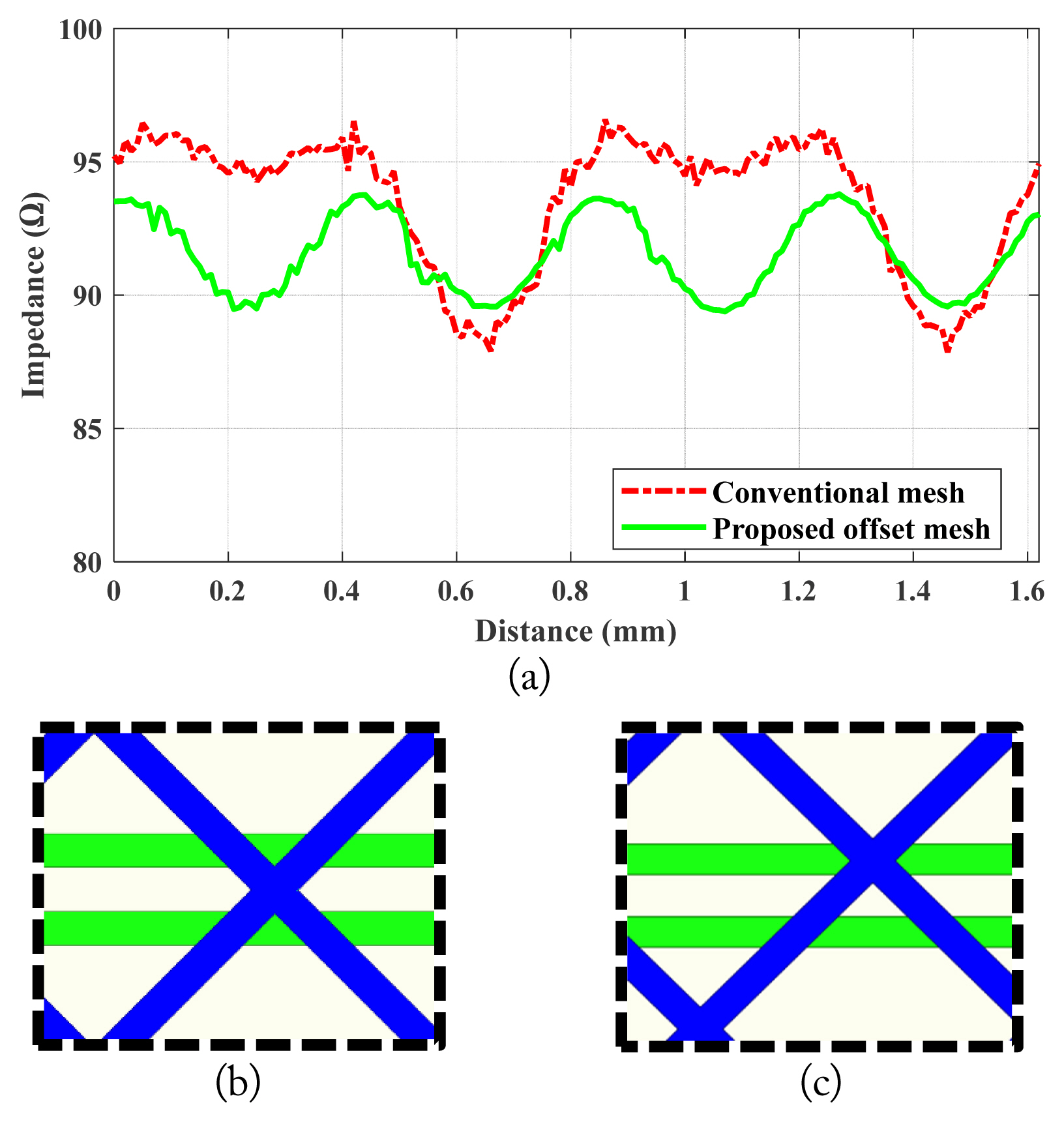
The apertures of a meshed ground plane cause changes in inductance and capacitance [6, 9]. A roundabout current path generated by apertures increases the inductance of the ground plane. In contrast, apertures reduce the capacitance value between the trace and the ground plane. An increase in the inductance and a decrease in the capacitance of a routed trace increases the impedance. Fig. 3 shows how the characteristic impedance variation at 10 GHz changes as we move the position of a differential pair in a finer step (163 positions in one period of the conventional mesh). As shown in Fig. 3(b), when the differential pair was placed near the point where the separations intersected, it had maximum impedance. Conversely, as shown in Fig. 3(c), the section between the maximum points had the minimum impedance value. As reported in [18], using our approach, we were able to reduce the difference between the maximum and minimum impedance, and our results showed more repeated maximum and minimum impedance values, as seen in Fig. 3(a). The variations in the conventional mesh and in the offset mesh were 8.7 Ω and 4.4 Ω, respectively. The differential impedance of the two traces was less affected by the position due to the differential signaling. The return current had two paths: the ground plane and an adjacent trace of the differential pair. The proportion of the return current in each path depended on the geometry of the channel [23].
2. Mode Conversion, Intra-pair Skew, and Inter-pair Skew
To evaluate mode conversion, the differential-to-common mode-conversion amount of mixed-mode S-parameters, Scd, is generally used [22]. A trace has different effective dielectric constants depending on whether it lands on a solid region or an aperture region. Using the stripline impedance equation in [10] to obtain the effective dielectric constants in the differential mode from the impedance values in the previous section, the conventional mesh had a value of 2.1 when the impedance was the maximum and 2.6 when the impedance was the minimum. In the case of the offset mesh, the values of the aforementioned variables were 2.25 and 2.5, respectively. The estimated impact of the effective dielectric constant variation Δɛreff on the differential signaling performance was given in [24, 25]. First, the variation was related to the speed of light, c0, the frequency, ω, and the phase constant, β, as shown in Eq. (1):
Then, we verified the conversion from the differential to the common mode %CM and the phase skew Tskew using Eq. (2):
and
where α is the attenuation constant, z is the physical location along the transmission lines, and βV and β&Vmacr; are the phase constants for signals V and V̄, espectively.
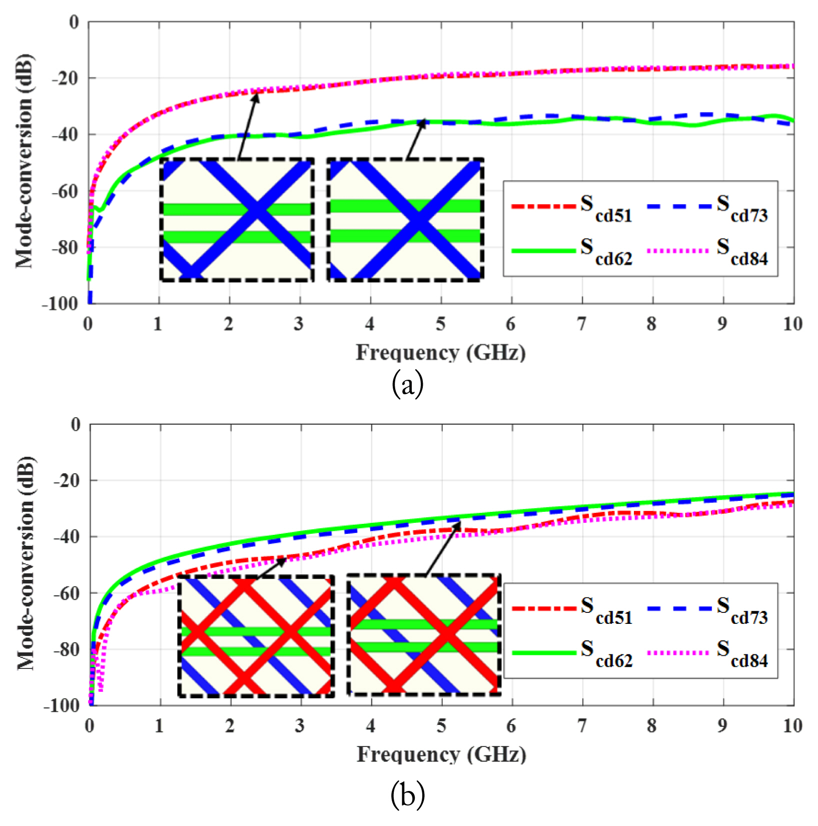
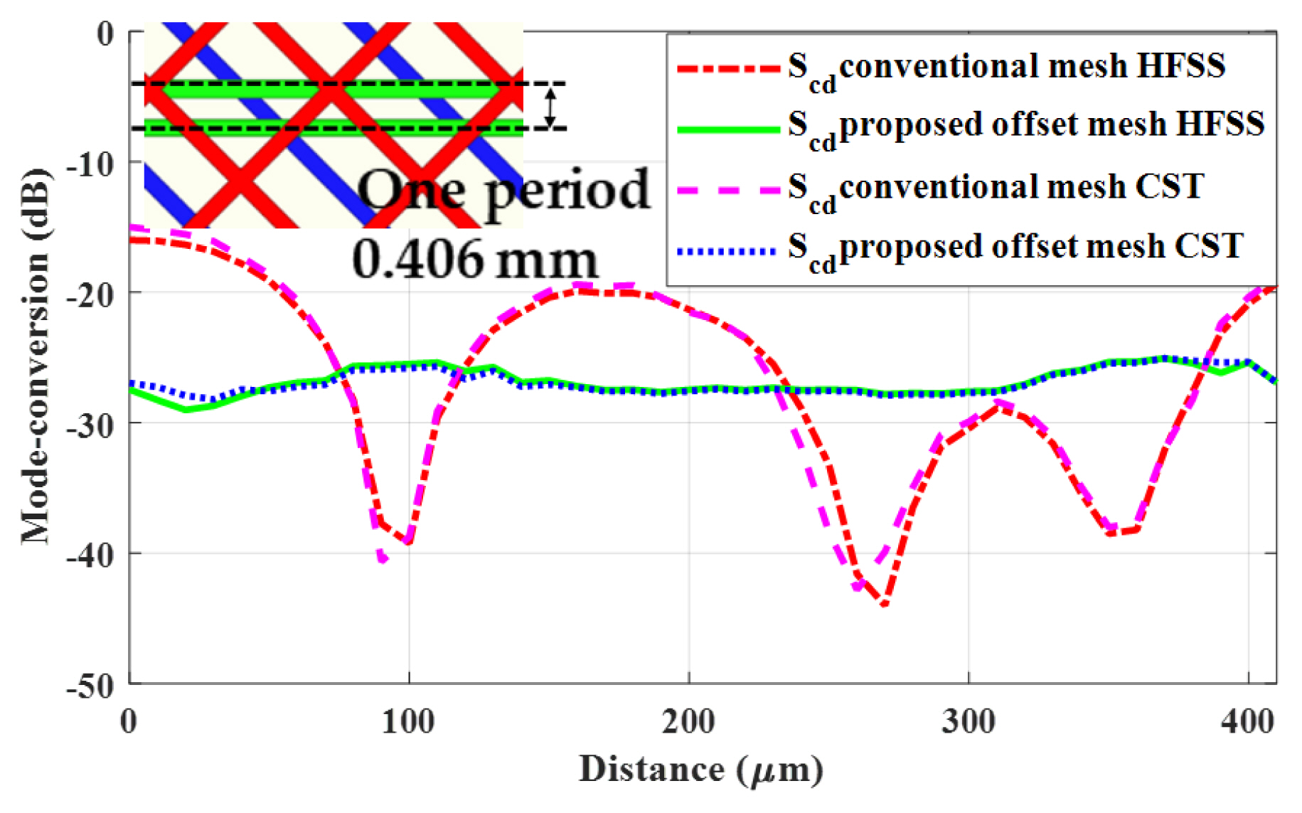
Fig. 4 compares the mode conversion of the two meshes. For the conventional mesh, the mode conversion was greater than −16 dB at 10 GHz in the worst case (see Scd51 or Scd84 in Fig. 4(a)). This happened when one of the two traces that consisted of a differential pair landed on a point where two separations intersected. In such a case, the two traces experienced very different effective dielectric constants, which resulted in an intra-pair skew and mode conversion. This can be greatly reduced by adopting the offset mesh. Fig. 4(b) shows that Scd51 and Scd84 were reduced by more than 10 dB. Although a differential pair was placed asymmetrically for the top mesh, this was compensated for at the bottom mesh.
Therefore, none of the four differential pairs exhibited significant mode conversion (approximately −25 dB at 10 GHz). The power sum of the common modes in the four pairs was smaller by one order of magnitude. Moreover, high-speed interconnection standards such as a USB, a display port, and HDMI had an Scd limit. It is important to meet each limit within the operating frequency range. For USB 3.1, 3.2, and 4 Gen 2, a mated cable assembly passed if the mode conversion was less than or equal to −20 dB from 100 MHz to 10 GHz [26, 27]. In the case of the mobile industry processor interface (MIPI) for D-PHY, no differential pair shall exceed −26 dB for frequencies below about 2 GHz [28]. Several of the routed buses on the conventional mesh were bound to exceed that limit, but all the routed buses on the proposed mesh met that limit due to their few changes depending on their location.
Fig. 5 shows how the extent of the mode conversion at 10 GHz changed as we moved the position of a differential pair in a finer step (48 positions in one period of the offset mesh). In the conventional mesh, a differential pair could exhibit more than −15 dB of mode conversion. However, with the proposed offset mesh, the differential pair exhibited consistently low (between −25 dB and −30 dB) mode conversion no matter where it was placed.
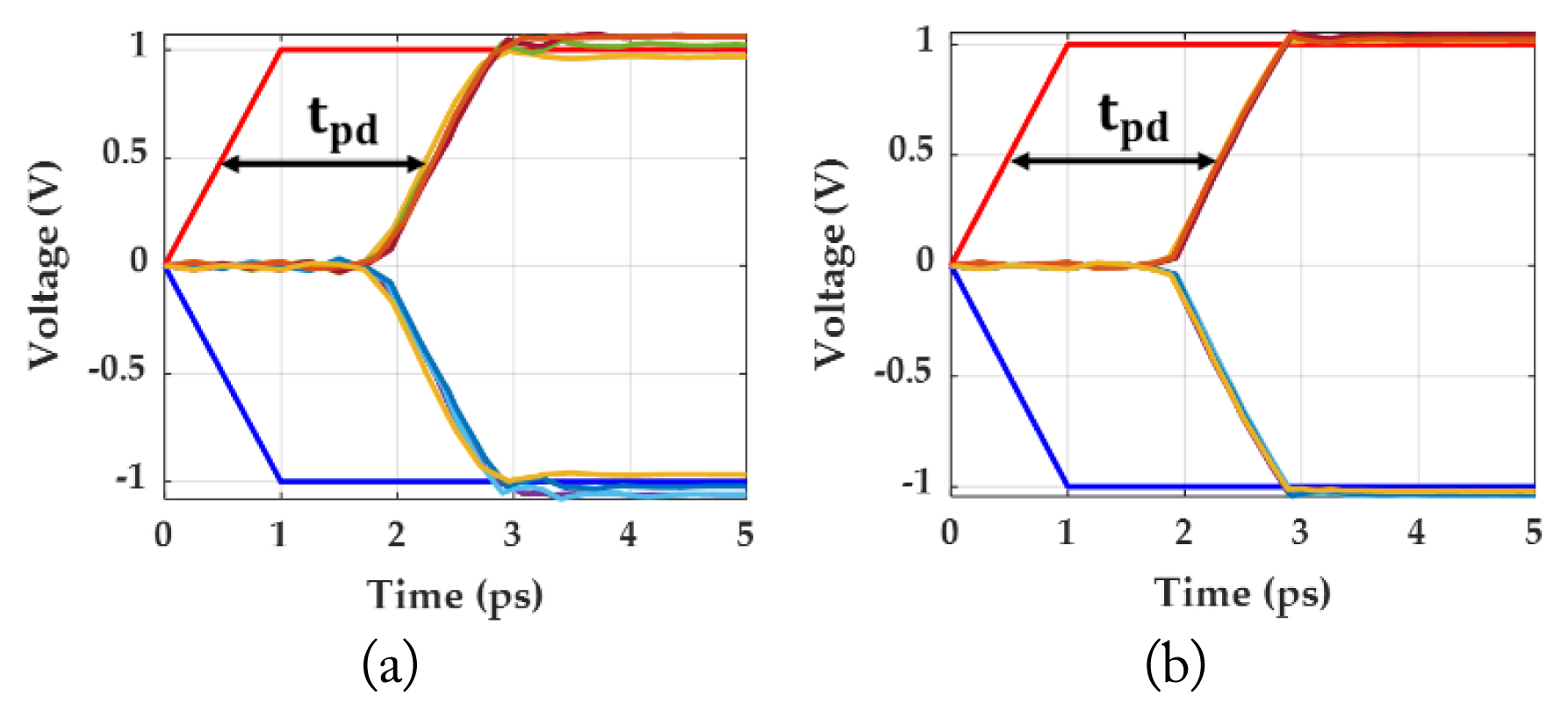
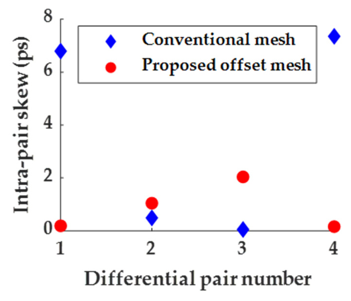
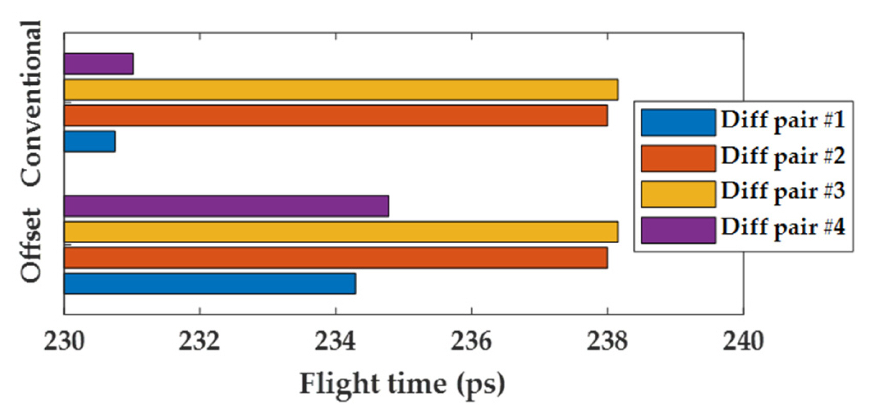
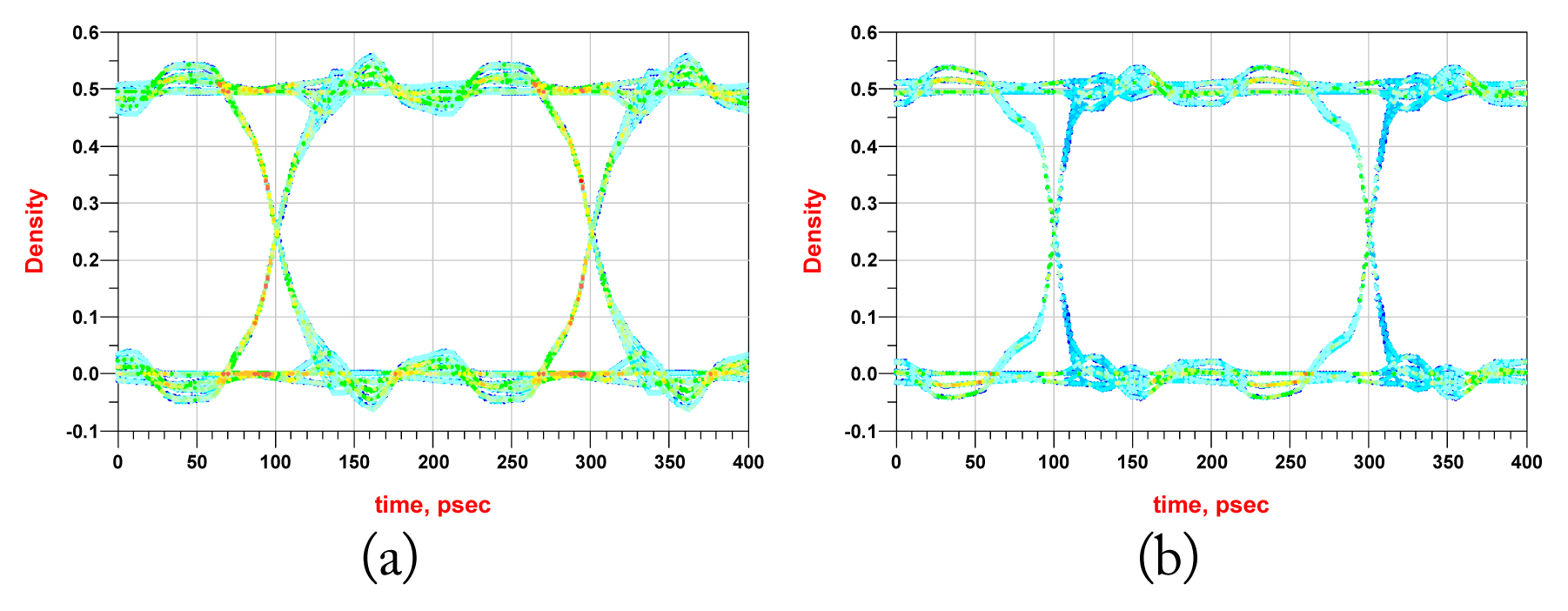
Figs. 6 and 7 show the transient simulation results of the intra-pair and inter-pair skews. The propagation delay, tpd, on the trace is the one-way from the source to the load time required by a signal to travel on that trace. It is a function of the dielectric constant. The difference in the propagation delay is called the skew. The skew between traces of a single differential pair is the intra-pair skew, and the skew between two or more differential pairs is the inter-pair skew. Therefore, the proposed offset mesh reduced the variation in the tpd by reducing the variation in the effective dielectrics seen on the two traces of each differential pair, as calculated by Eq. (3). Fig. 8 shows that while the conventional mesh had the worst-case intra-pair skew of 7.4 ps, that of the offset mesh was only 2.0 ps. The inter-pair skew between the differential pairs #1 and #2 in the conventional mesh was 7.4 ps. It was reduced to 3.8 ps by adopting the offset mesh in Fig. 9. The eye diagrams were simulated using a pseudorandom bit sequence (PRBS) pattern and a bit rate of 5 Gbps. The eye diagram that evaluated the differential signal integrity is shown in Fig. 10 and Table 1. The eye diagram of the offset mesh showed better eye quality than that of the conventional mesh.
IV. Conclusion
The proposed offset mesh structure enabled two striplines of a differential pair in an FPCB to have the same number of ground traces no matter where they were placed. The offset mesh was implemented without the additional design elements that are required in the conventional mesh structure. As a result, the mode conversion and the intra-pair and inter-pair skews were greatly reduced. Moreover, a uniform insertion loss was identified at any location, and the characteristic impedance variation was significantly reduced. The proposed offset mesh even showed better performance in terms of insertion loss, which gave it better signal integrity and routing flexibility.