A Compact Ultra-Wideband Chip Antenna with Bandwidth Extension Patch and Simple Isolator for MIMO Systems for Mobile Handheld Terminals
Article information
Abstract
A compact ultra-wideband (UWB) chip antenna that has high isolation for multi-input multi-output (MIMO) systems is presented in this paper. The antenna is composed of a chip antenna, a printed circuit board, and an isolator stub. High isolation was obtained using a simple stub, and a low-frequency band was extended by applying a bandwidth extension patch to the chip antenna. The pulse performance of the proposed antenna was measured by changing the angle of the receiving antenna. The proposed antenna was simulated by applying a hand phantom. The effect of the grip position of the hand phantom on the reflection coefficient, isolation, and gain was analyzed. The measured impedance bandwidth was 2.45 GHz to 9 GHz. The proposed UWB MIMO antenna has a high isolation, greater than 25 dB, at the operating frequency. The antenna gain varied from 3 dBi to 4.5 dBi over the operating frequency range. The measured group delay variation was less than 1 ns. The measured pulse features have negligible chirp and a small dispersion.
I. Introduction
Ultra-wideband (UWB) technology was first introduced in 1962, and UWB-related technology has rapidly developed since the late 1980s. In particular, UWB technology is applied to military communication requiring high security and surface penetration radars. In 2002, the Federal Communications Commission terminated civilian use regulations to enable wireless communications only within 9 m of indoor environments. UWB communication technology has become a very attractive technology in modern wireless communication systems because of its advantages: a high data rate, interference immunity to multipath propagation, low power consumption, omnidirectional radiation patterns, and wide bandwidths [1]. The UWB communication system allows wireless data transmission and reception between devices and can be applied to smart home networks, such as multimedia content, electronic product operation, and security. Therefore, UWB antennas have been actively researched as the most important element affecting UWB data transmission and reception [2–8]. To reduce the size of the antenna and obtain UWB characteristics, a ring resonator and a matching stub were used, and a notch stub was added inside the ring resonator to remove the IEEE 802.11a frequency band [2]. In [3], UWB characteristics were obtained using trapezoid-shaped patches and steps, and various types of notch slots were formed inside the patch. The semi-circle slot UWB antenna is miniaturized by configuring matching steps, a trapezoidal patch, and hat-shaped notch slots inside the semi-circle slot [4]. The UWB chip antenna induces a coupling phenomenon by inserting a diagonal slot on the patch surface to obtain miniaturization and broadband [5]. A UWB antenna using a band-pass filter (BPF) is a structure that passes a desired band by connecting a 3-channel BPF to the UWB antenna [6]. To selectively acquire different notch band bandwidths, the quadruple-band notch UWB antenna is composed of a trapezoidal patch, quadruple notch slot, filter, and complementary split-ring resonator [7]. The UWB monopole antenna can control the return loss by varying the shape of the cactus-shaped monopole [8]. In UWB antenna technology, the multi-input multi-output (MIMO) antenna system is a technique for improving high-speed communication while increasing data capacity and efficiency. The MIMO system is a multi-antenna signal processing method for transmitting and receiving data using multiple antennas in a mobile communication environment [9]. MIMO technology has the advantage of broadening the range of wireless communication and significantly improving the speed by transmitting two or more data signals in the same radio channel using several antennas.
However, as MIMO systems use multiple antennas, electromagnetic interference can occur between antennas. Interference between antennas reduces the performance of each antenna (voltage standing wave ratio [VSWR], gain, and efficiency) and affects the overall MIMO system performance. To avoid mutual interference, the distance between the antennas should be at least λ/2. However, if the distance between the antennas increases, the size of the mobile terminal increases, and application to a mobile handheld terminal becomes difficult. Therefore, many studies have been published to reduce mutual interference while maintaining the performance of the antenna and miniaturizing the antenna [10–14]. In the dual-band notched UWB antenna, two antenna elements with a compact size of 5.5 mm × 11 mm are connected to two protruded ground parts, respectively, and a notch characteristic is obtained using a metal strip and an open slot [10]. The UWB MIMO antenna improves the isolation characteristics by inserting a tree-shaped structure between triangular patches [11]. The UWB MIMO antenna using a quasi-self-complementary antenna (QSCA) consists of two QSCA monopoles, which can easily achieve UWB operation. By arranging the two monopoles symmetrically, with their main radiation directions oppositely oriented, a UWB MIMO antenna with high isolation has been proposed [12]. The study in [13] improved the isolation of the UWB MIMO antenna by using a carbon black film, which could absorb electromagnetic signals. The surface of the MIMO antenna element (18 mm × 20 mm) was covered by a polystyrene block with a cylindrical hole, and a thin graphite sheet fixed with a polystyrene cylindrical block was fabricated in the column hole [14].
To improve the isolation characteristics of MIMO antennas, methods such as adjusting the separation distance between each antenna, inserting a decoupling circuit, and directly connecting a suspended line between the antenna patches can be used [15–17]. However, adjusting the spacing between the antennas has a disadvantage, as it may reduce the isolation limit and the antenna’s performance, and it can relocate the antenna every time the antenna is applied to the mobile handheld terminal. In addition, the method of inserting a decoupling circuit and a suspended line can be applied only to a single frequency, as it is difficult to apply in broadband and multiband antennas. In contrast to the isolation enhancement technique, the method of deforming the ground plane by inserting slits and stubs on the ground plane can improve isolation because each antenna appears to have independent ground planes [18–20].
In this paper, we present a compact UWB chip antenna with sector-shaped and bandwidth extension (BWE) patches. We improved the bandwidth of the proposed chip antenna by using sector-shaped and BWE patches on the printed circuit board (PCB) pad and partial ground plane. The proposed UWB chip antenna operates in the frequency band of 2.45 to 9 GHz, and the measured group delay variation is less than 1 ns. The pulse characteristics were simulated and measured, and they had a small dispersion and negligible chirp. We used four UWB chip antennas for the application of mobile handheld terminals in MIMO systems and added a simple stub to the ground plane to improve isolation without affecting the reflection coefficient characteristics. We performed the simulation by applying a hand phantom to analyze the performance of the MIMO antenna when a hand is placed on the chip antenna.
II. UWB Chip Antenna Design and Experimental Results
Conventional UWB chip antennas use a dielectric with a high dielectric constant to reduce the size of the antenna and cannot cover the entire UWB frequency band, owing to their small size compared to the wavelength [5].
The proposed antenna improves the bandwidth by adding a BWE patch to the bottom of the chip antenna. We extended the bandwidth of the lower band without changing the antenna’s size and shape. Fig. 1 shows the geometry of the UWB chip antenna. The proposed antenna is composed of a chip antenna and a PCB (30 mm × 30 mm). The size of the chip antenna is 10 mm × 10 mm, and it consists of a sector-shaped patch, a via, and a chip pad. The PCB consists of a BWE patch, a microstrip (MS) feed line, and a partial ground plane. The proposed antenna uses FR4 dielectric substrates with a dielectric constant of 4.4 and a thickness of 0.8 mm for both the chip antenna and the PCB. A sector-shaped patch is located on the top of the chip antenna, and a chip pad attached to the BWE patch is located on the bottom plane. The sector-shaped patch is electrically connected to the BWE patch by the via hole, and the signal is applied through the MS feed line. The BWE patch with the MS feed line is located on the PCB, and the partial ground plane is located on the bottom plane. A typical UWB antenna forms a notch slot or stub on the radiation patch plane to reject a 5- to 6-GHz frequency band. In this study, it is not necessary to redesign the notch slot, even if the shape of the chip antenna element has been changed by configuring the notch slot on the BWE patch plane.
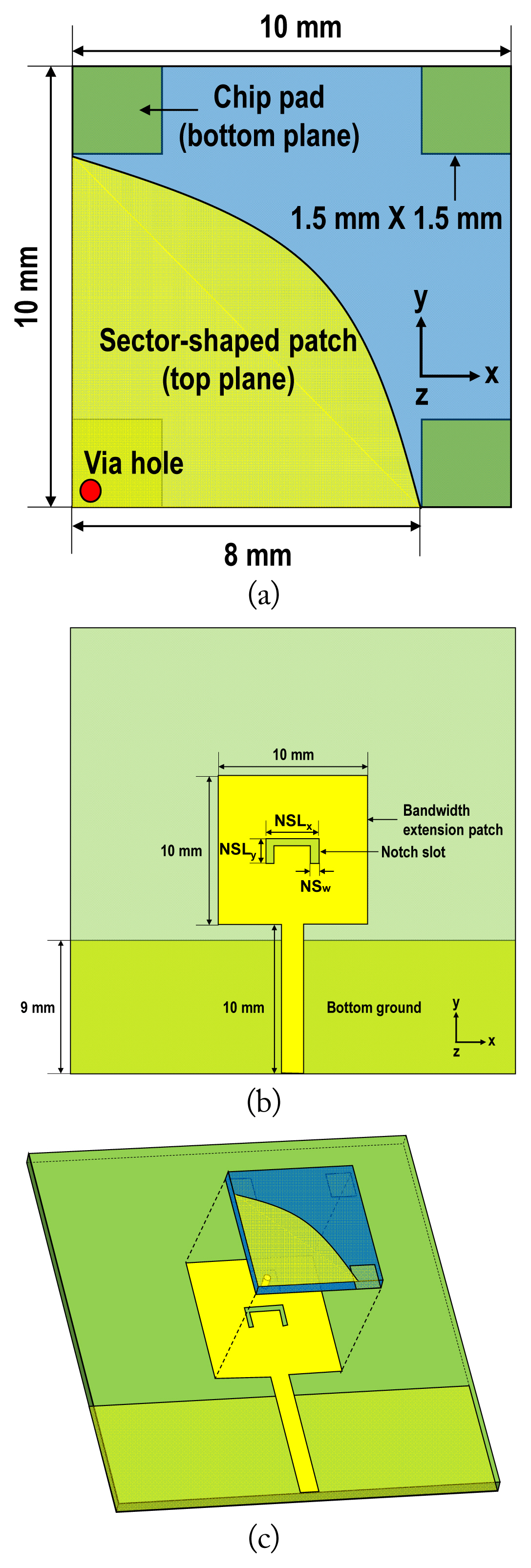
Proposed UWB antenna: (a) chip antenna, (b) PCB plane, and (c) the combination should be a combined chip antenna with PCB.
Fig. 2 shows the simulated and measured results of the reflection coefficient and group delay. The UWB chip antenna was evaluated using a vector network analyzer (Anritsu MS46122A) in an anechoic chamber. Fig. 2(a) shows the reflection coefficient of the proposed antenna. As shown in the figure, when only the chip antenna elements are used, the frequency band of 4 to 9.8 GHz is satisfied. However, with the BWE patch, the low-frequency band is extended to obtain the 2.45- to 9-GHz frequency band. Fig. 2(b) shows the simulation results of the frequency characteristics according to the change in the horizontal length of the notch slot. The width of the notch slot is calculated as follows [21]:
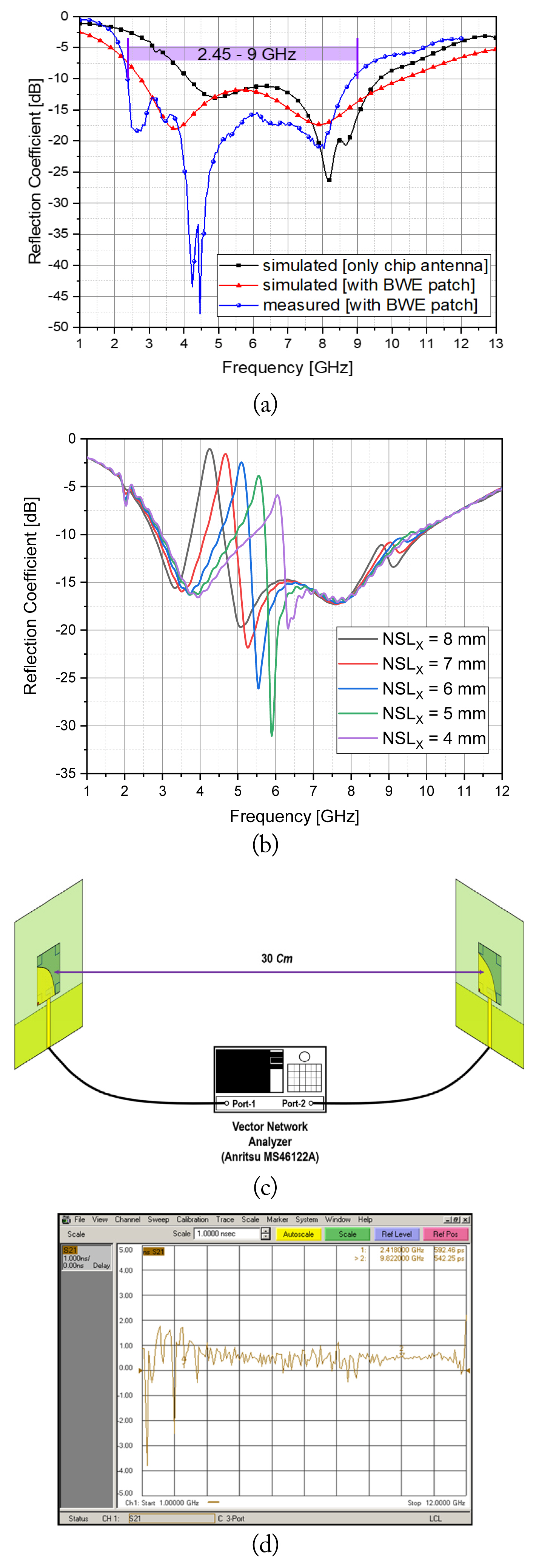
Simulated and measured results: (a) reflection coefficient without notch slot, (b) reflection coefficient with notch slot, (c) group delay set-up, and (d) group delay.
Here, Z0 is 100 Ω, h is the substrate thickness, ɛr and λ0 are the substrate permittivity and wavelength, respectively, and w is the slot width. The notch slot length is λ0/4 at 5.5 GHz. The total length of the notch slot (NSLX + (NSLY × 2)) is 10 mm. The slot width (NSW) based on Eq. (1) is 0.38 mm. As shown in Fig. 2(a), as the length of the notch slot increases, the notch frequency band moves to the lower band. The simulation results confirmed that we could adjust the rejection frequency band by changing the slot length. In this study, only the notch characteristics were confirmed through simulation, and the fabrication and measurement led to a structure without a notch slot. For the group delay measurement, the measurement environment was set up as shown in Fig. 2(c). We connected the transmit/receive antennas to the vector network analyzer ports 1 and 2, separated the two antennas by a distance of 30 cm [22], and measured the group delay characteristics. Fig. 2(d) shows the measured group delay, and the group delay variation is less than 1 ns in the operating frequency.
Fig. 3 shows the simulation and measurement of radiation patterns at 3, 5, 7, and 9 GHz in the yz- and xz-planes. The experimental results for the radiation patterns were obtained in an anechoic chamber. The radiation patterns are similar to those of a conventional dipole antenna in the yz-plane and an omnidirectional antenna in the xz-plane. The antenna gain variation in the operating band is 2 dBi, and the antenna gain varies from 1 to 3 dBi over the operating frequency range.

Simulated and measured radiation patterns: (a) yz-plane and (b) xz-plane.
The most important factor in UWB communication systems is minimal pulse distortion. The measurement setup for measuring the pulse characteristics of the UWB chip antenna is shown in Fig. 4(a). The transmitting antenna is connected to the pulse generator (PulsON200), and the receiving antenna is connected to a digital oscilloscope (TDS6604). A digital oscilloscope has a 20 GS/s sampling rate and a 6 GHz bandwidth [2]. Fig. 4(b) shows the source signal of the pulse generator for the simulated and measured Tx/Rx characteristics of the UWB chip antenna. The Gaussian pulse used for the measurements had a pulse width of 600 ps and a peak amplitude of 1 V. The proposed chip antenna is characterized for different orientations of the receiving antenna. The receiving antenna is fixed in the vertical (θ) direction and positioned at 0°, 30°, 60°, 90°, 120°, 150°, and 180° in the horizontal (Φ) direction. Fig. 4(c)–4(i) shows the received signal from the proposed UWB chip antenna as a function of horizontal rotation (Φ). The impulse response of the UWB chip antenna is a damped sinusoid with a duration of approximately 0.5 ns and a measured peak amplitude of approximately 1.5 mV in all cases. The measured received signals rarely show a reflected signal without dispersion. Therefore, the UWB chip antenna provides an exceptionally clean transient response. The proposed chip antenna has excellent pulse characteristics despite being a compact dielectric patch antenna [21].

Measured pulse characteristics: (a) experimental setup, (b) source signal of pulse generator, (c) ϕ = 0°, (d) ϕ = 30°, (e) ϕ = 60°, (f) ϕ = 90°, (g) ϕ = 120°, (h) ϕ = 150°, and (i) ϕ = 180°.
III. Design of UWB MIMO Antenna using Simple Isolator Stub and Experimental Results
To verify the MIMO characteristics of the proposed UWB chip antenna, we simulated the isolation characteristics according to the antenna positions in four cases. The proposed UWB chip antenna with a 2 × 2 chip size is located inside the mobile terminal. Simulations were performed using the Ansys High-Frequency Structural Simulator (HFSS). We selected the best position of the antenna element by comparing the coupling coefficient (isolation) of each case.
Fig. 5(a)–5(d) shows four cases depending on the antenna position. Fig. 5(e)–5(h) shows the coupling coefficients for the four cases. As shown in the figure, the coupling characteristics of case 2 (Fig. 5(f)) and case 3 (Fig. 5(g)) are relatively good. However, we chose case 3 because it has the best overall isolation characteristics over 3 GHz.
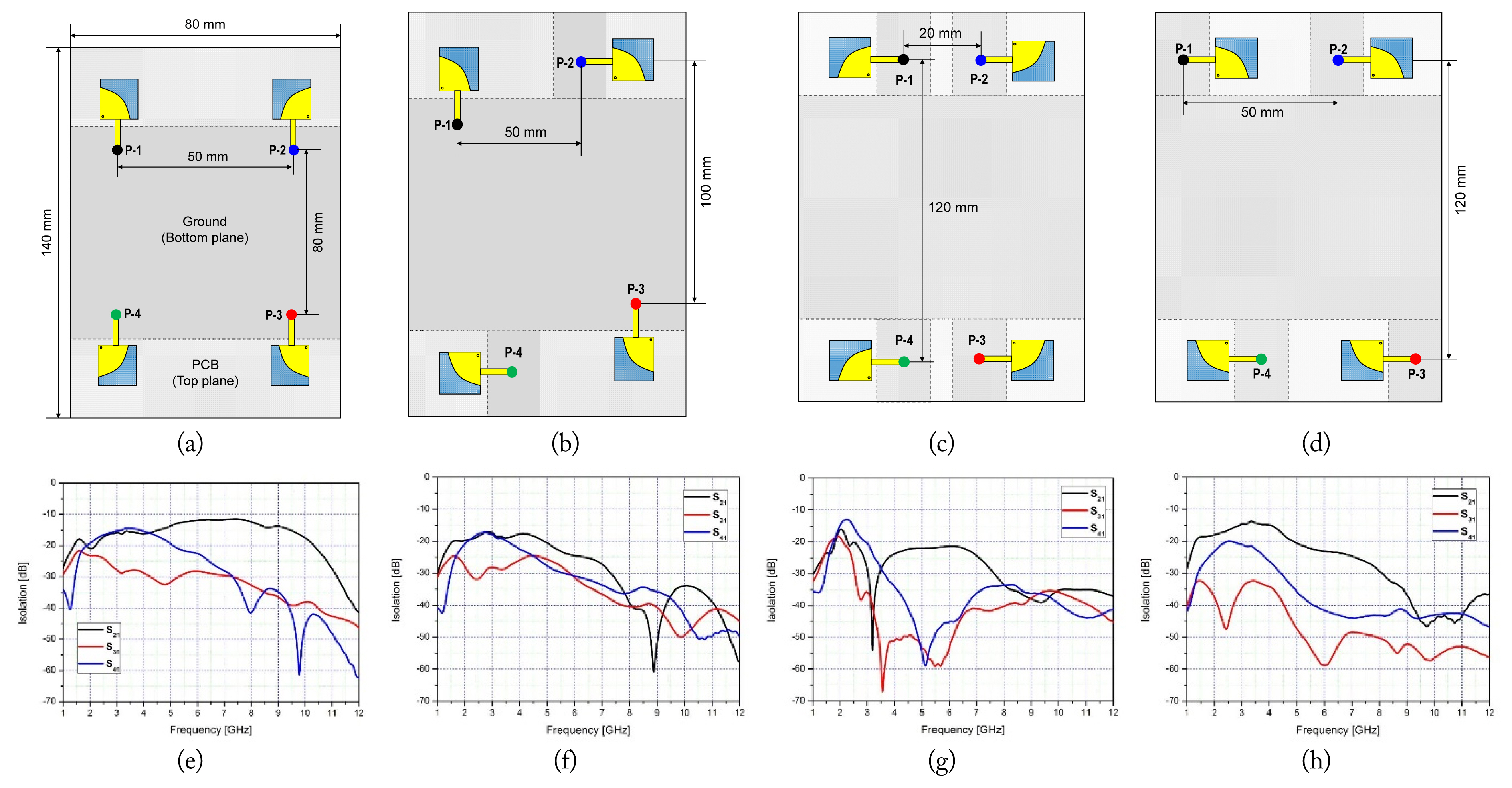
Comparisons of simulated isolation of the proposed UWB MIMO antenna: (a) configuration of case 1, (b) configuration of case 2, (c) configuration of case 3, (d) configuration of case 4, (e) isolation of case 1, (f) isolation of case 2, (g) isolation of case 3, and (h) isolation of case 4.
Fig. 6 shows the addition of a simple isolation stub to improve the isolation characteristics. Fig. 6(b) shows a prototype with a simple isolation stub at each end of the bottom ground plane based on the structure of case 3. As shown in the results of Fig. 5(g), the isolation characteristics are poor in the 2- to 3-GHz frequency band. In addition, the isolation characteristics of S21 are poor in the 4- to 7-GHz frequency band. Fig. 6(c) shows the measurement of the isolation characteristics of the proposed antenna with the addition of a simple isolation stub. As shown in the figure, the 2- to 3-GHz frequency band isolation has improved, and the S21 characteristics have also improved.
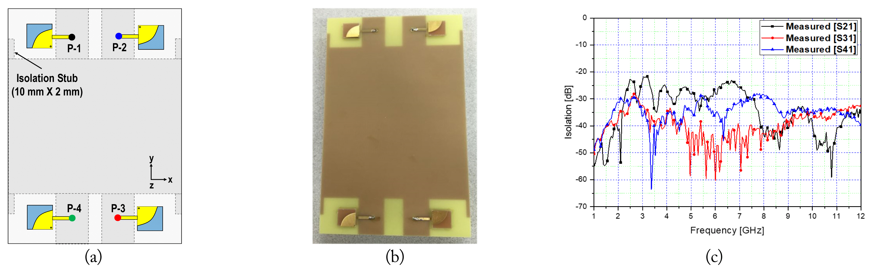
UWB MIMO antenna with isolation stub: (a) antenna structure, (b) photograph, and (c) measured isolation.
We simulated the E-field and surface current using Ansys HFSS to analyze the effect of a simple isolation stub on isolation. Fig. 7 shows the E-field and surface current distribution simulation results with and without a simple isolation stub, respectively. As shown in the figure, without a simple isolation stub, the E-field and surface currents distributed vertically along the bottom ground side plane affect the antenna via port 4. With a simple isolation stub, the E-field and surface currents that exited at port 1 mostly focused on simple isolation stubs.
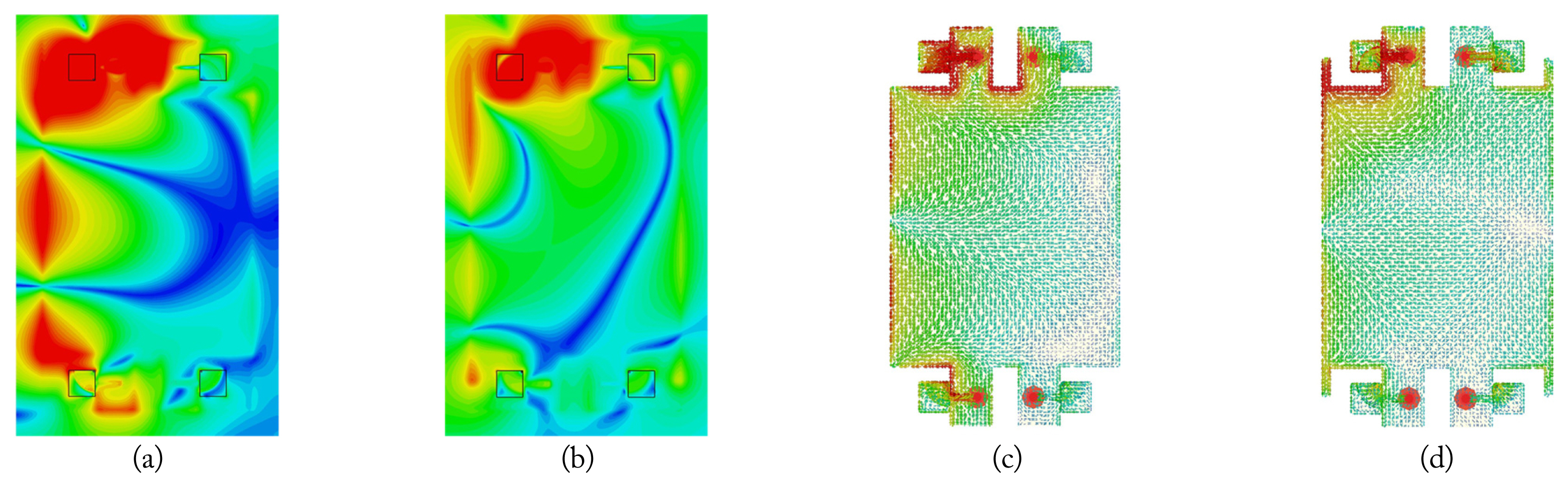
Simulated E-field and surface current at 3 GHz: (a) E-field without isolation stub, (b) E-field with isolation stub, (c) surface current without isolation stub, and (d) surface current with isolation stub.
The measured radiation patterns of the proposed UWB MIMO antenna at 3, 5, 7, and 9 GHz are plotted in Fig. 8. We measured the patterns for the xz- and yz-planes at 3, 5, 7, and 9 GHz on all ports (1 to 4). The radiation patterns of the proposed UWB MIMO antenna are typical compared with those of conventional MIMO antennas. An independent pattern is formed for each port. Although there is a change in the pattern according to the measurement plane (xz- and yz-planes), the pattern for each port (1 to 4) in the same measurement plane is opposite in direction but has the same shape.

Measured radiation patterns of the proposed MIMO antenna with the isolation stub: (a) xz-plane at port 1, (b) xz-plane at port 2, (c) xz-plane at port 3, (d) xz-plane at port 4, (e) yz-plane at port 1, (f) yz-plane at port 2, (g) yz-plane at port 3, and (h) yz-plane at port 4.
IV. Specific Absorption Rate Characteristics of Hand Phantom
To analyze the characteristics of the UWB MIMO antenna when located in a hand, a hand phantom simulation of the proposed antenna was performed. The mobile terminal was modeled to embed the proposed antenna into the mobile terminal.
The mobile terminal included a mobile case, LCD panel, and battery. The mobile case was made of polycarbonate (ɛr = 2.8, loss δ = 0.009), and the LCD panel and battery were perfect conductors. The hand phantom was modeled using dielectric materials that mimic the human skin (ɛr = 5, loss δ = 0.05, and material density = 1,000 kg/m3) and blood (ɛr = 42, loss δ = 0.99, and material density = 1,000 kg/m3). Fig. 9 shows the specific absorption rate (SAR) simulation model and the simulated 1-g SAR values for the UWB MIMO antenna. The SAR values were simulated using the IEEE C95.3 averaging method, and the input power for the SAR simulation was 0.126 W (24 dBm) for the full band (2.45 to 9 GHz) [23, 24]. We performed the simulation for three cases (only the antenna, with a mobile case, and with the hand phantom). Subsequently, we analyzed the characteristics according to the position of the hand grip when the mobile case was applied.
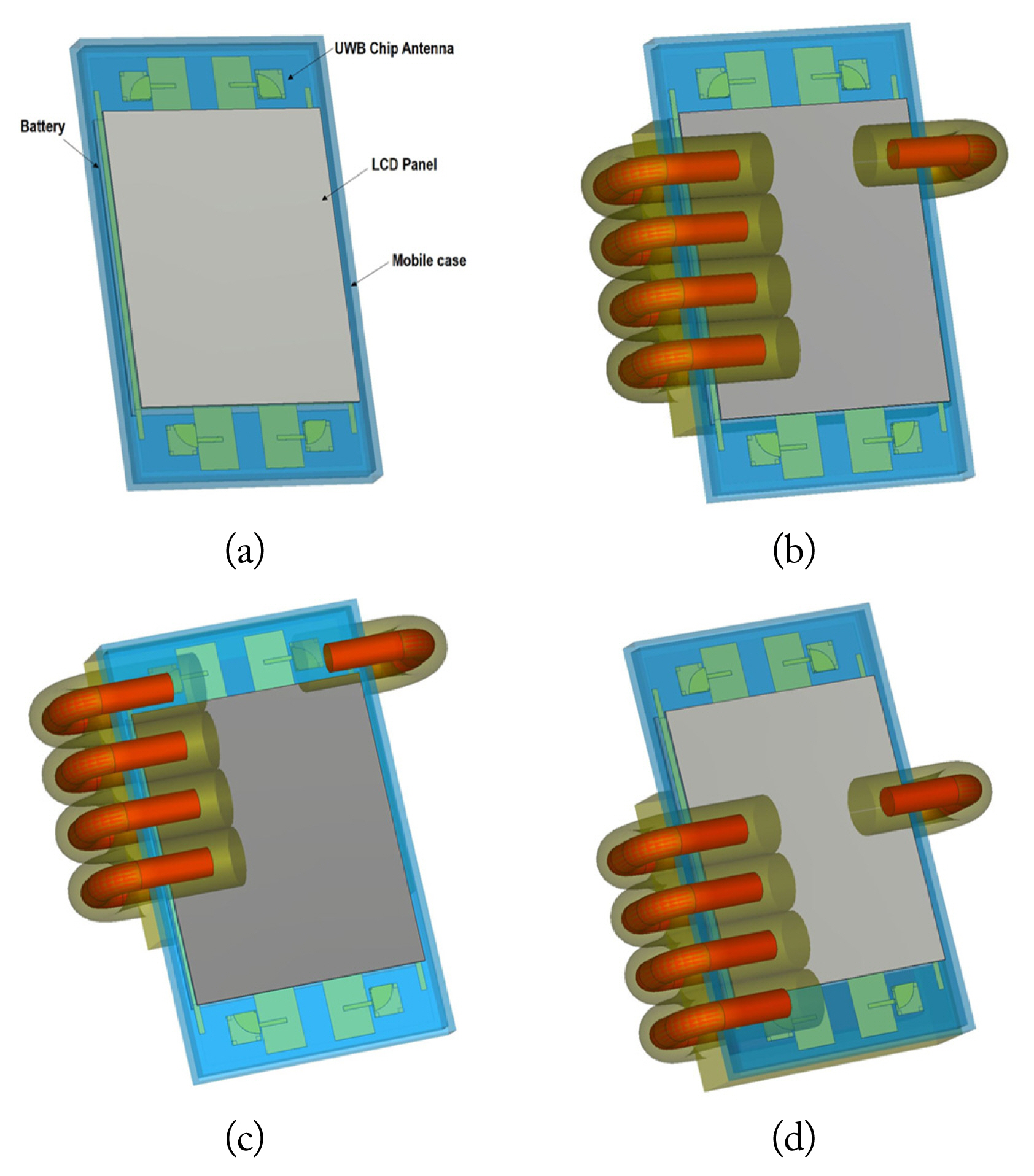
SAR simulation modeling: (a) mobile case, (b) hand-phantom, (c) top position, and (d) bottom position.
Fig. 10 shows the simulated reflection coefficient and isolation (S21–S41) resulting from five cases. As shown in Fig. 10(a), with the mobile case and hand phantom applied, the reflection coefficient around 3 GHz increased to approximately −6 dB. However, in frequency bands above 3 GHz, the reflection coefficient was more than −10 dB. Fig. 10(b)–10(d) shows the isolation characteristics of the five cases. Although the isolation values increased near 2 GHz for the mobile case and hand phantom, the isolation value was typically above −20 dB at higher frequencies.
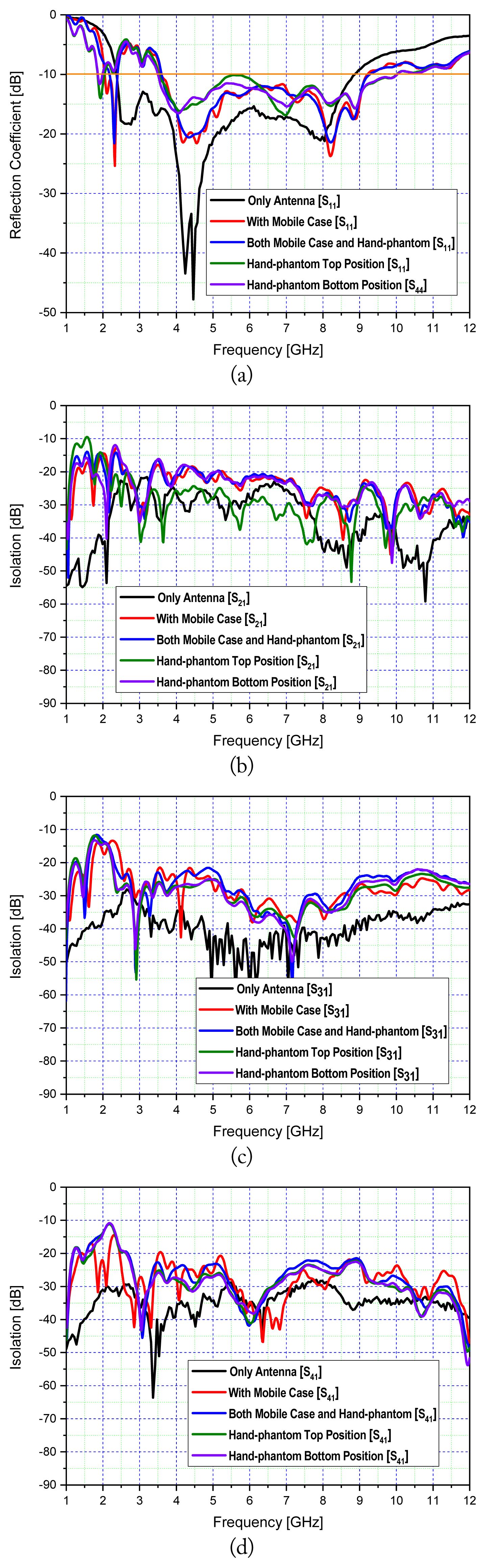
Measured and simulated reflection coefficient and isolation: (a) reflection coefficient, (b) S21, (b) S31, and (d) S41.
Fig. 11 shows the changes in 3D radiation patterns with the position of the hand phantom grip. Here, the simulation frequency was 5 GHz, and the changes in 3D radiation patterns are shown at P-1 and P-4 with center, top, and bottom hand phantom grips. Fig. 11(a) and 11(b) shows the 3D radiation patterns when the hand phantom was located in the center position. It can be seen that the hand phantom did not affect the radiation pattern, and the maximum power was radiated in each chip antenna’s (P-1 and P-4) direction. Fig. 11(c) and 11(d) shows the 3D radiation patterns when the hand phantom was at the top position. The hand phantom affected the top-position antennas, and the radiated power of the 1-chip antenna (left top side) connected to the P-1 feed line was reduced. Fig. 11(e) and 11(f) shows the 3D radiation patterns when the hand phantom was at the bottom position. The hand phantom affected the bottom-position antennas, and the radiated power of the 4-chip antenna (right bottom side) connected to the P-4 feed line was reduced.
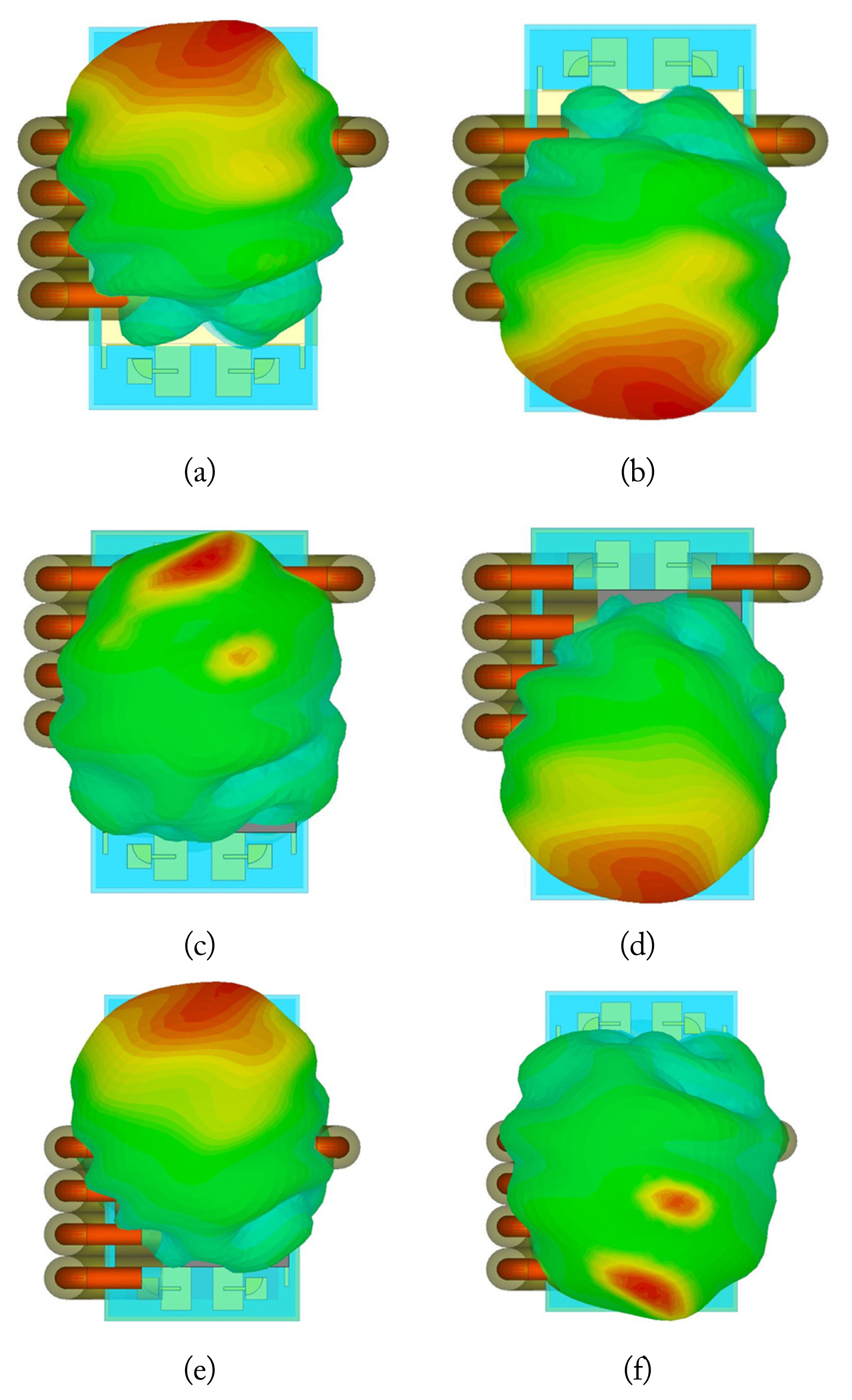
Simulated radiation patterns for hand phantom position: (a) center position at 5 GHz (P-1), (b) center position at 5 GHz (P-4), (c) top position at 5 GHz (P-1), (d) top position at 5 GHz (P-4), (e) bottom position at 5 GHz (P-1), and (f) bottom position at 5 GHz (P-4).
Fig. 12 shows the antenna gains for the simulated and measured results at P-1 and P-4 for five cases. Only the antenna was measured, and the remainder (with mobile case and hand phantom) were simulated. As shown in Fig. 11, the antenna gains in the area where the hand phantom grip was located decreased drastically.
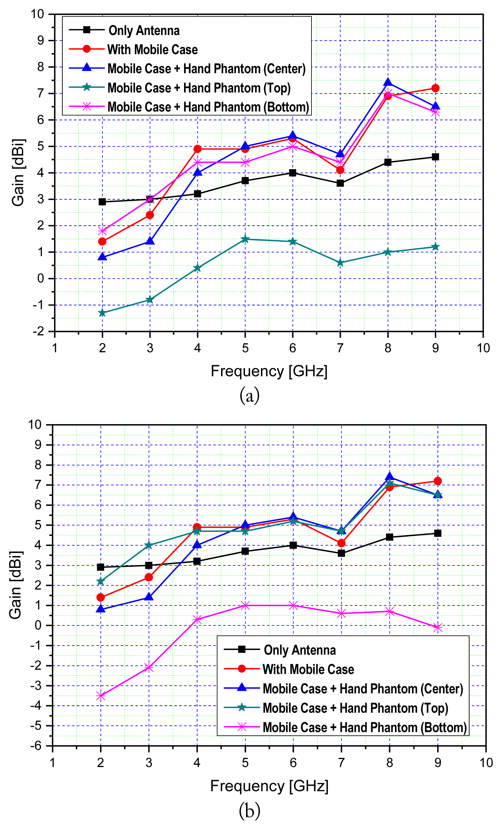
Measured and simulated antenna gains: (a) port 1 and (b) port 4.
Table 1 shows a comparative summary of the fundamental properties of the proposed antenna with the reported UWB MIMO antennas available in the references [25–29]. When compared with the reported antennas, the proposed antenna has a simple and compact structure, as shown in Table 1.

Comparison of existing and proposed UWB antenna
V. Conclusion
A compact UWB chip antenna with high isolation for MIMO systems for mobile handheld terminals was designed and presented in this study. The proposed UWB chip antenna was designed with a simple structure that satisfied the UWB characteristics even though it was implemented in a compact size. The isolation between antennas in close proximity to each other was improved by adding a simple stub instead of a complicated structure. To analyze the characteristics of the UWB MIMO antenna when the antenna was positioned in the hand phantom, we analyzed the reflection coefficient, isolation, radiation pattern, and gain for different positions of the hand phantom. The proposed UWB MIMO antenna exhibited excellent MIMO performance regardless of the hand phantom grip position.
Acknowledgments
This work was supported by an Institute for Information & Communications Technology Promotion (IITP) grant funded by the Korean government (MSIT) (No. 2022-0-00218, Specialty Laboratory for Wireless Backhaul Communications based on Very High Frequency).
References
Biography

Jung-Nam Lee received his B.S. and M.S. degrees from the Department of Information and Communication Engineering, Hanbat National University, Daejeon, Korea, in 2004 and 2006, respectively. He received his Ph.D. degree in Radio Wave Engineering from Hanbat National University in 2010. Since 2011, he has been with the Electronics and Telecommunications Research Institute (ETRI), Daejeon, Korea, where he is currently a senior researcher. His research interests include small antennas, millimeter wave antennas, terahertz antennas, RFID antennas, UWB antennas, beam-forming antennas, and small base station antenna design.

Seok Bong Hyun received his B.S., M.S., and Ph.D. degrees in physics from the Korea Advanced Institute of Science and Technology (KAIST) in 1991, 1993, and 1998, respectively. In 1999, he joined the Electronics and Telecommunications Research Institute (ETRI), Korea, where he is currently a principal researcher. His research interests include the design of millimeter waves and very high-speed wireless network systems.

Young-Kyun Cho received a B.S. degree in electrical and electronics engineering from Ajou University, Suwon, South Korea, in 2001, an M.S. degree in electrical and electronics engineering from the Pohang University of Science and Technology, Pohang, South Korea, in 2003, and a Ph.D. degree in electrical and electronics engineering from Chungnam National University, Daejeon, South Korea, in 2019. He was a Principal Researcher with the Electronics and Telecommunications Research Institute (ETRI), Daejeon. Currently, he is an assistant professor of electrical, electronics and control engineering with Kongju National University. His research interests include novel devices, mixed signal circuits, Nyquist and oversampling rate data converters, dc–dc converters for integrated circuits and RF components, mm-wave & sub-THz systems, and semiconductor antennas for high-frequency systems. Dr. Cho was the recipient of the Best Paper Award at the IEEE Nanotechnology Materials and Devices Conference in 2006, the Outstanding Employee Award by ETRI in 2015, and was twice awarded the Minister of Knowledge Economy and President Prize of the Republic of Korea at the National Semiconductor Design Contest in 2009 and 2014, respectively.