Analysis of Hot Carrier Degradation in 0.25-μm Schottky Gate AlGaN/GaN HEMTs
Article information
Abstract
In this work, we report hot carrier-induced degradation in normally-on AlGaN/GaN high electron mobility transistors (HEMTs) with a 0.25-μm gate. To analyze the hot carrier effect, the semi-on state stress test was carried out and the DC and pulsed I-V characteristics were analyzed. The stress condition was set at the gate voltage of −3.8 V and the drain voltage of 40 V, where the drain current was at 10% of the maximum. After a stress test, the positive shift of the threshold voltage was observed and the drain current was decreased by 19%. In addition, the gate and drain lag phenomena were pronounced when measured by the pulse with a 1.23% duty cycle. The device degradation can be attributed to the hot electron-induced trapping during the semi-on stress test, which imposed the high electric field and the low channel temperature in the device.
I. Introduction
An AlGaN/GaN high electron mobility transistor (HEMT) is a III-V compound semiconductor device to be used in the field of radio frequency (RF) and high-power applications as it has the material properties of wide bandgap, high critical electric field and velocity saturation compared to silicon and GaAs [1–4]. In addition, the two-dimensional electron gas (2DEG) is formed at the AlGaN/GaN heterojunction due to the spontaneous and piezoelectric polarizations, resulting in the high electron mobility and normally-on operation [5].
While the device performance is important for commercialization of AlGaN/GaN HEMT for RF and power applications, the strong reliability is also another requirement to be fulfilled. Since an AlGaN/GaN HEMT can be operated at a high voltage with high frequency compared with the conventional counterpart, the hot electron effect is inevitable. Therefore, investigating the hot electron effect in the short channel AlGaN/GaN HEMT is essential.
In this paper, we analyzed the degradation characteristics induced by the semi-on state stress test in which the hot electron generation is enhanced thanks to a high electric field with the low channel current (i.e., low channel temperature).
II. Device Structure and Methodology
The structure of the AlGaN/GaN HEMTs fabricated using the cleanroom process is shown in Fig. 1. The devices consisted of a buffer layer with 1.75 μm thickness, a 300-nm i-GaN, a 1-nm AlN, a 12-nm Al0.3Ga0.7N, a 2.5-nm GaN cap, and a SiN passivation [6]. The devices had a gate length of 0.25 μm, a gate width of 100 μm, and the spacing of the gate-source and gate-drain was 1 μm and 2.75 μm, respectively. To analyze the hot carrier effect, the semi-on stress test was performed using Keithley’s 4200A-SCS with an auto-sequence. The stress duration was 1,800 seconds, and DC characteristics were measured after each duration to analyze the device degradation. In the AlGaN/GaN HEMT, it is difficult to observe the bell-shape form of IG-VG characteristics often observed in AlGaAs/GaAs HFET, which is a typical signature of hot electron effect [7]. The drain stress voltage was 40 V, which is below the breakdown voltage, to provide a high electric field along the channel. A gate voltage of −3.8 V was determined to set the drain current at 10% of the maximum. This semi-on condition can be in favor of the hot electron generation, which requires the high electric field and a certain number of electrons to be accelerated. As shown in Fig. 2, the pulsed I-V was measured with a 1.23% duty cycle, 30-μs period, 350-ns width, and a 20-ns rise and fall time, which was compared before and after stress.
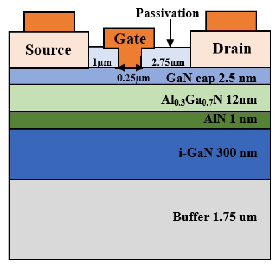
Cross-sectional schematic of AlGaN/GaN HEMT.
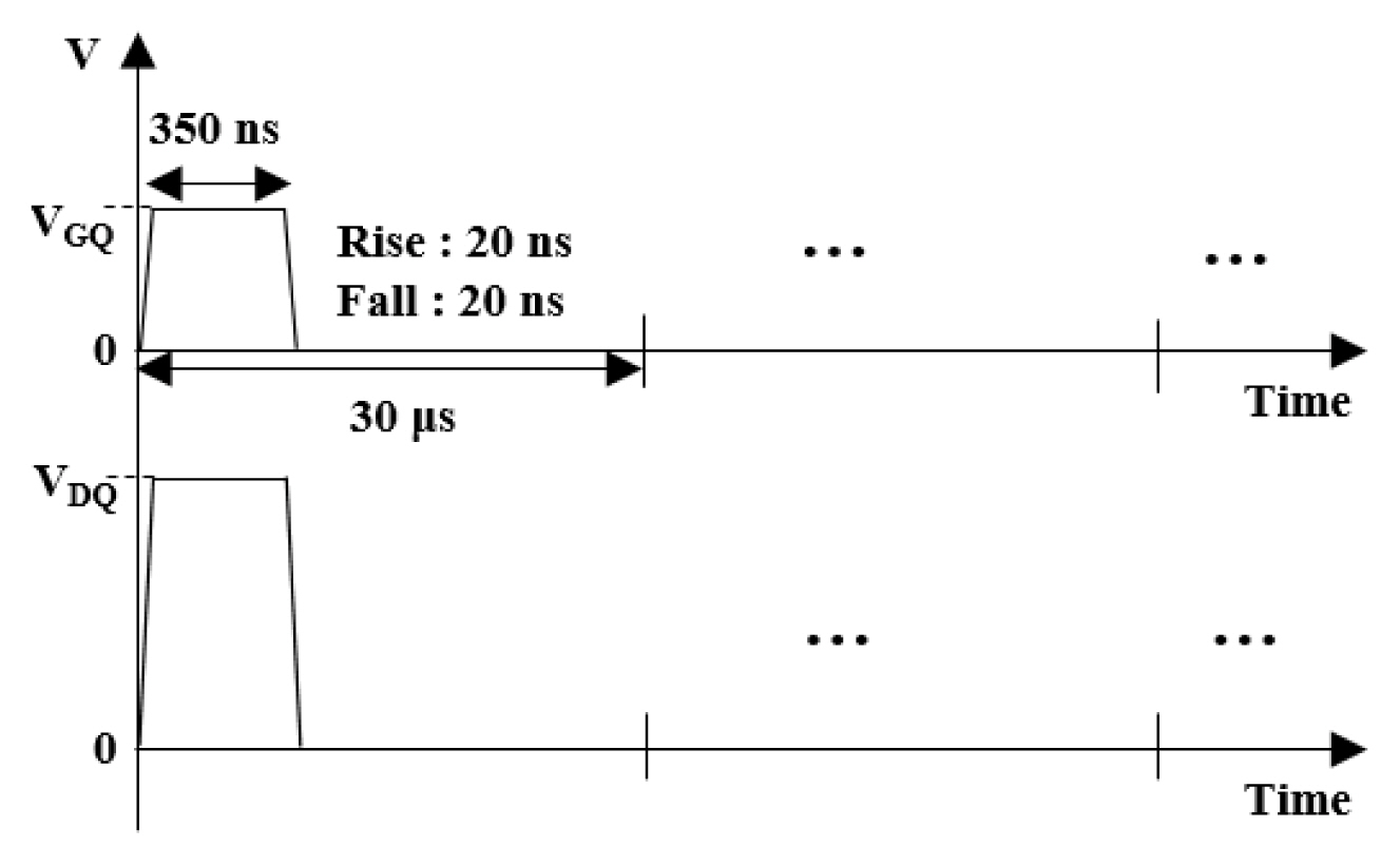
Pulse measurement condition.
III. Measured Results
The transfer characteristics before and after the semi-on stress were measured at VD = 1 V. As shown in Fig. 3(a), a threshold voltage extracted using linear extrapolation method from the fresh device was −4.05 V, with a maximum transconductance (Gm,max) of 263 mS/mm, and a maximum drain current (ID,MAX) of 370 mA/mm. After a 180-minute semi-on stress, the threshold voltage was positively shifted to −3.7 V, with a reduced Gm,max and ID,MAX of 230 mS/mm and 300 mA/mm, respectively. It corresponds to approximately 12.5% and 19% reduction compared to the pre-stress characteristics. The leakage current was significantly increased due to the increase of the gate leakage current by the degradation. As shown in Fig. 3(b), the output characteristics were also degraded after the stress test. The time-dependent characteristics of the device parameters are shown in Fig. 4. As the semi-on stress progressed, drain current was gradually decreased and the threshold voltage showed a positive shift indicating that electrons were trapped underneath the gate region.
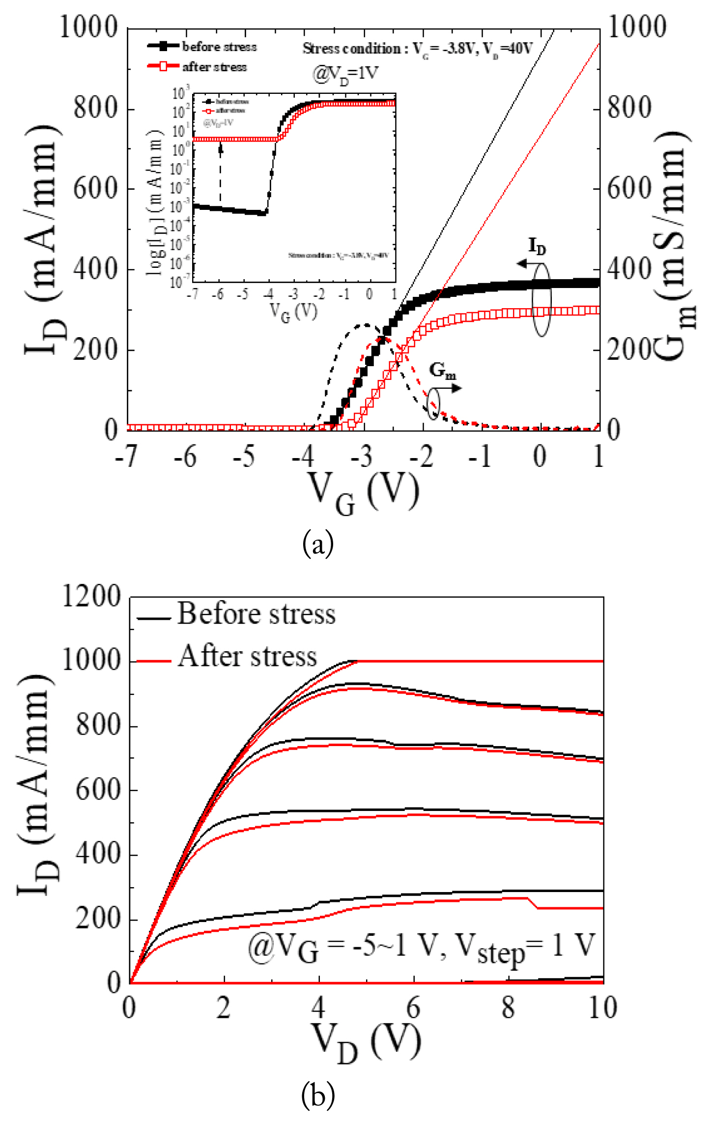
I-V characteristics of the AlGaN/GaN HEMT before and after semi-on stress at VG = −3.8 V and VD = 40 V: (a) transfer characteristics with a transconductance (the line is a tangent line at maximum Gm) and (b) output characteristics.
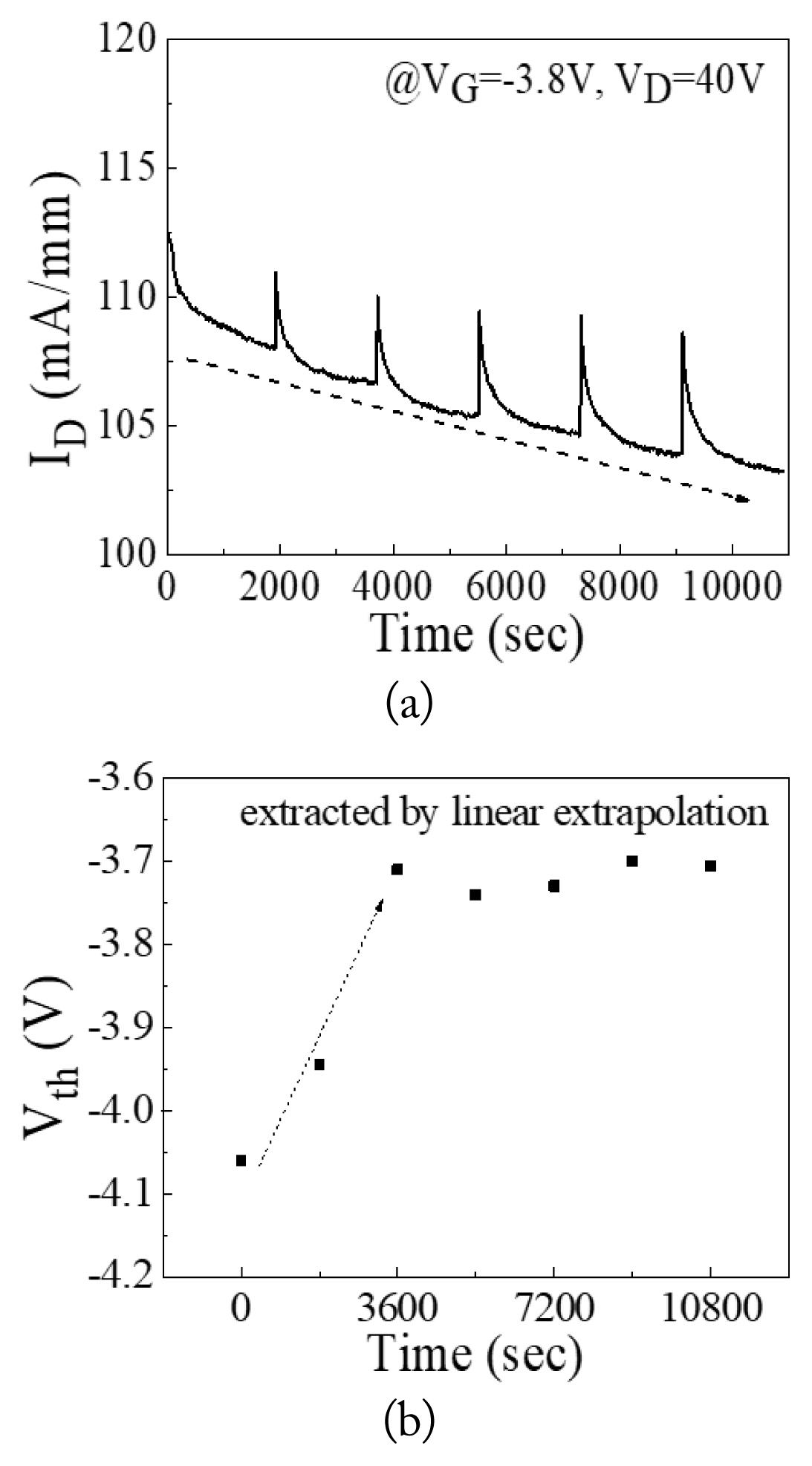
Time-dependent parameter change of AlGaN/GaN HEMT during semi-on stress: (a) drain current and (b) distribution of threshold voltage.
During the stress test, energetic electrons can be injected into the traps under the gate and the surface states in the gate-drain access area. Trapped electrons will cause the depletion of 2DEG channel gradually as the stress test progresses. The positive shift of the Vth can be attributed to the trapped electrons underneath the gate region. The trapping process seems to become saturated under the gate region earlier than in the G-D access region, because the LG is much shorter than LGD.
To evaluate the electron trapping effects, the gate lag and drain lag were investigated through pulsed I-V measurements. Various characterization methods have been utilized to investigate the trapping effect of AlGaN/GaN HEMTs [8–12]. For example, Klein et al. [9] investigated the deep traps in GaN metal-semiconductor field-effect transistors by means of the spectral dependence of the optical quenching measurements, and Zhang et al. [10] characterized interface acceptor-like traps by pulse-drain-voltage measurements. In addition, Kim et al. [11] observed that the trapping phenomenon was more pronounced in the GaN HEMT submitted to hot electron stress by means of the gate lag measurement and deep level transient spectroscopy. Larger discrepancy between DC and the pulsed I-V was attributed to the traps generated by the hot electron effect. The gate and drain lag measurement has been widely accepted as an efficient tool to probe the trapping effect in GaN HEMT devices since Binari et al. [12] characterized the effects of the surface and buffer traps on the microwave performance. The pulsed ID-VD characteristics of fresh and stressed devices are shown in Fig. 5(b), where the quiescent bias point (Q-point) is at the gate voltage of −10 V and the drain voltages of 10 V and 20 V. The pulsed I-V characteristics revealed the larger gate and drain lags after stress.
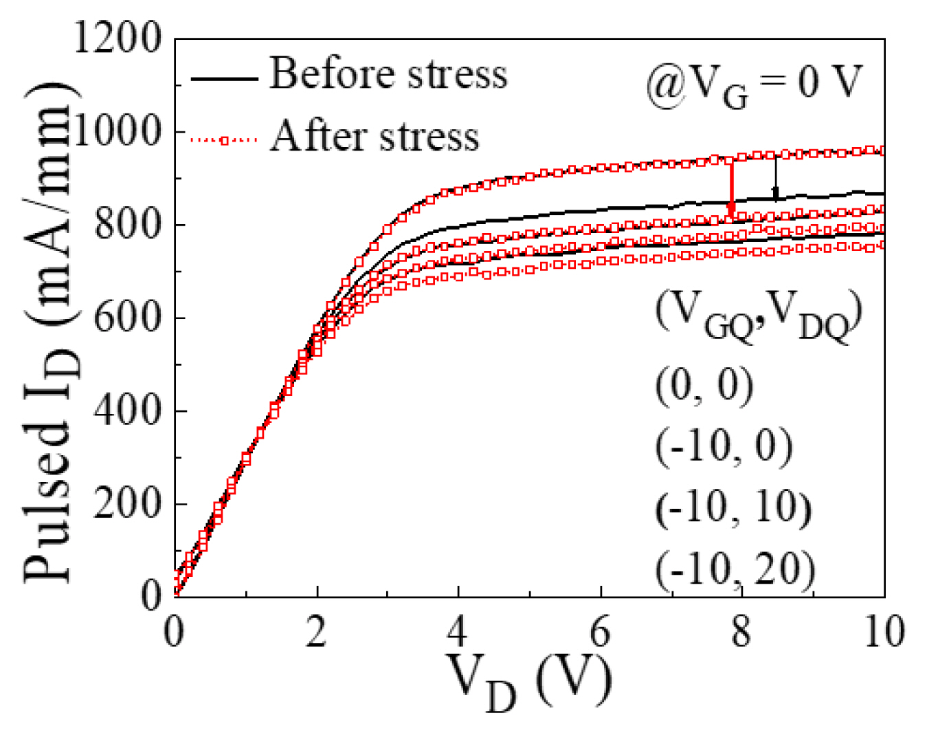
The pulsed ID-VD characteristics before and after the semi-on stress.
The gate lag before stress was 9.5% and increased to 13.1% after stress. The gate-drain lag at VGQ = −10 V and VDQ = 20 V before the stress was 18.4% and increased to 21% after stress caused trapping in the buffer layer. As shown in Fig. 6, lucky electrons gain high energy while drifting across the channel and are injected into the AlGaN layer under the gate causing the positive shift of the Vth. Hot electrons can also be trapped into the buffer layers and aggravates gate-drain lag phenomenon. Temperature dependence of the hot electron-induced degradation should be analyzed to clarify the hot electron effect.
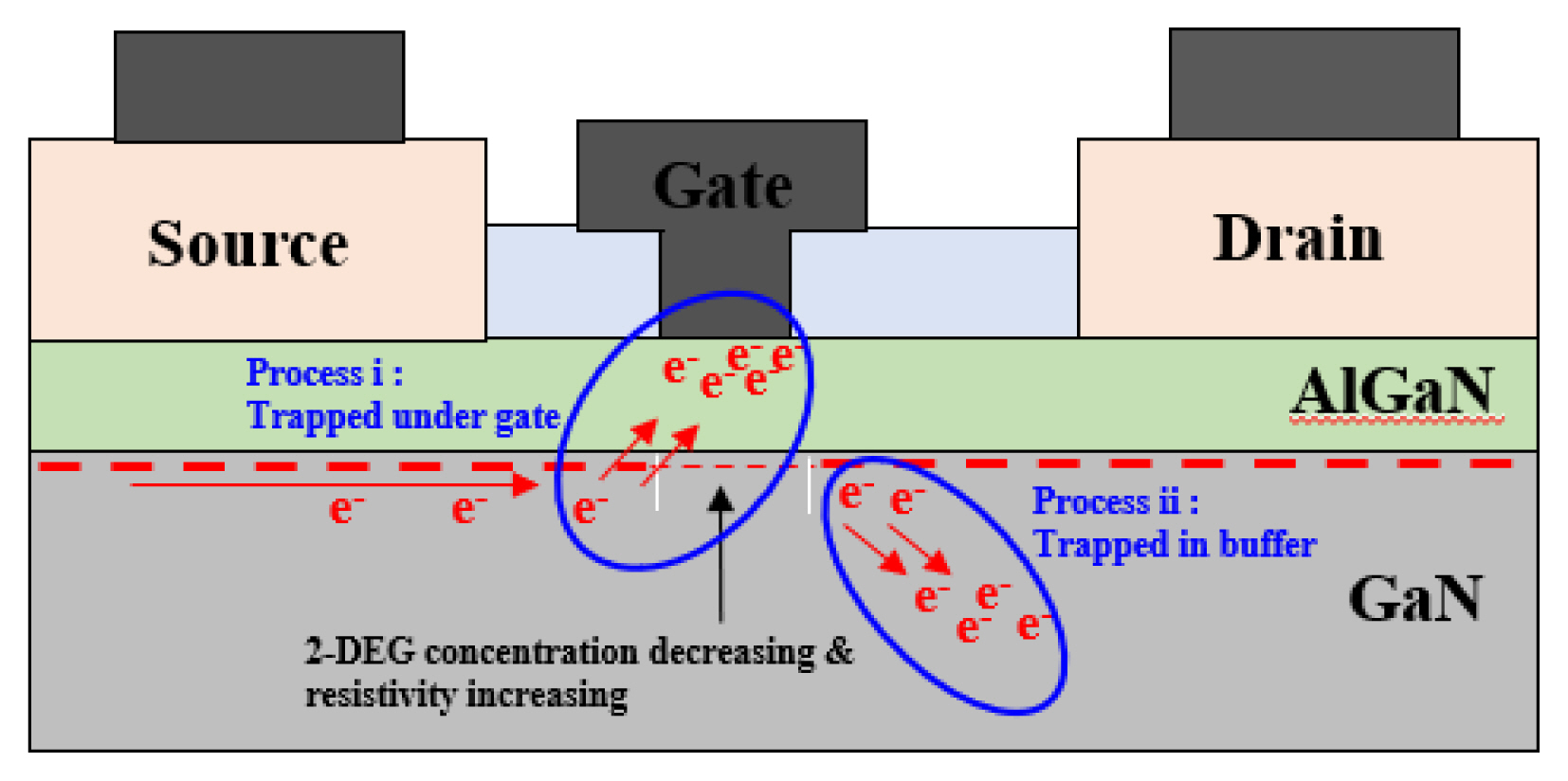
Cross-sectional schematic of degradation mechanism by hot carrier.
IV. Conclusion
This work presents the hot carrier-induced degradation in the AlGaN/GaN HEMTs based on the semi-on stress tests. The degradation characteristics include the positive shift of Vth and the larger gate-drain lag, suggesting that the electron trapping was facilitated by the stress test. The Vth shift is attributed to hot electrons trapped in the AlGaN barrier under the gate. Hot-electron trapping in the buffer worsened the gate-drain lag.
Acknowledgments
This work was supported by Institute for Information & Communications Technology Promotion (IITP) grant funded by the Korea government (MSIP) (No. 2021-0-00760) and Basic Science Research Programs (No. 2015R 1A6A1A0303183331 and 2021R1F1A1051094) through the National Research Foundation of Korea (NRF).
References
Biography

Seong-In Cho received his B.S. and M.S. degrees in electronic and electrical engineering from Hongik University, Seoul, Korea, in 2019 and 2021, respectively. His research interests relate to the analysis of the reliability of gallium nitride devices. He is currently with the foundry division in Samsung electronics.

Won-Ho Jang received his B.S. and M.S. degrees in electronic and electrical engineering from Hongik University, Seoul, Korea, in 2016 and 2018, respectively. He is currently pursuing the Ph.D. degree at Hongik University. His research interests include the analysis of gallium nitride devices.

Ho-Young Cha received his B.S. and M.S. degrees in electrical engineering from the Seoul National University, Seoul, Korea, in 1996 and 1999, respectively, and a Ph.D. degree in electrical and computer engineering from Cornell University, Ithaca, NY, in 2004. He was a Postdoctoral Research Associate with Cornell University until 2005, where he focused on the design and fabrication of wide bandgap semiconductor devices. He worked with the General Electric Global Research Center, Niskayuna, NY, from 2005 to 2007, developing wide-bandgap semiconductor sensors and high-power devices. Since 2007, he has been with Hongik University, Seoul, where he is currently professor in the School of Electronic and Electrical Engineering. His research interests include wide-bandgap semiconductor devices. He has authored over 130 publications in his research area.

Hyungtak Kim received his B.S. degree in electrical engineering from Seoul National University, Seoul, Korea and a M.S./Ph.D. degrees in electrical and computer engineering from Cornell University, Ithaca, New York, USA, in 1996 and 2003, respectively. In 2007, he joined the School of Electronic and Electrical Engineering at Hongik University, Seoul, Korea and is currently a professor. His research interests include the reliability physics of semiconductor devices and their applications in extreme environment electronics. Prior to joining Hongik University, he spent 4 years developing CMOS devices and process integration for DRAM technology as a senior engineer in the semiconductor R&D center at Samsung Electronics, Co. Ltd.