I. Introduction
Since 5GŌĆÖs commercialization, the number of 5G users has been increasing rapidly. 5G users are predicted to account for 45% of global mobile data traffic by 2025 [1]. According to the 3rd Generation Partnership Project (3GPP), 5G new radio (NR) n257 (26.5ŌĆō29.5 GHz), n258 (24.25ŌĆō27.5 GHz), n259 (39.5ŌĆō43.5 GHz), n260 (37ŌĆō40 GHz), and n261 (27.5ŌĆō28.35 GHz) bands are allocated as high-frequency 5G bands. Furthermore, several countries have adopted 5G NR n257, n258, and n261 (24.25ŌĆō29.5 GHz) bands as high-frequency 5G bands [2]. It is important to consider that these bands enable the handling of tremendous amounts of 5G data traffic and offer an improved 5G experience. Most research on 5G antennas has used stacked structure or cavities to enhance bandwidth and consider 5G bands [3ŌĆō7]; however, this structure requires an additional substrate or structure, which results in higher manufacturing costs. To avoid this, a single substrate and direct feeding method are recommended. The wireless communication antenna must be considered for high-gain and high cross-polarization discrimination (XPD) [8, 9].
In this study, a 2 ├Ś 16 array antenna with a direct microstrip line feed and parasitic elements was fabricated on a single substrate for 5G NR n257, n258, and n261 bands (24.25ŌĆō29.5 GHz); the proposed antenna exhibited high XPD and high gain. A single Rogers RT/Duroid 5880 substrate (╔ør = 2.2, tan╬┤ = 0.0009) was used. A wide bandwidth was achieved by using gap-coupled parasitic elements. Moreover, high XPD values were achieved due to the use of orthogonal dual polarization.
II. Antenna Configuration and Design
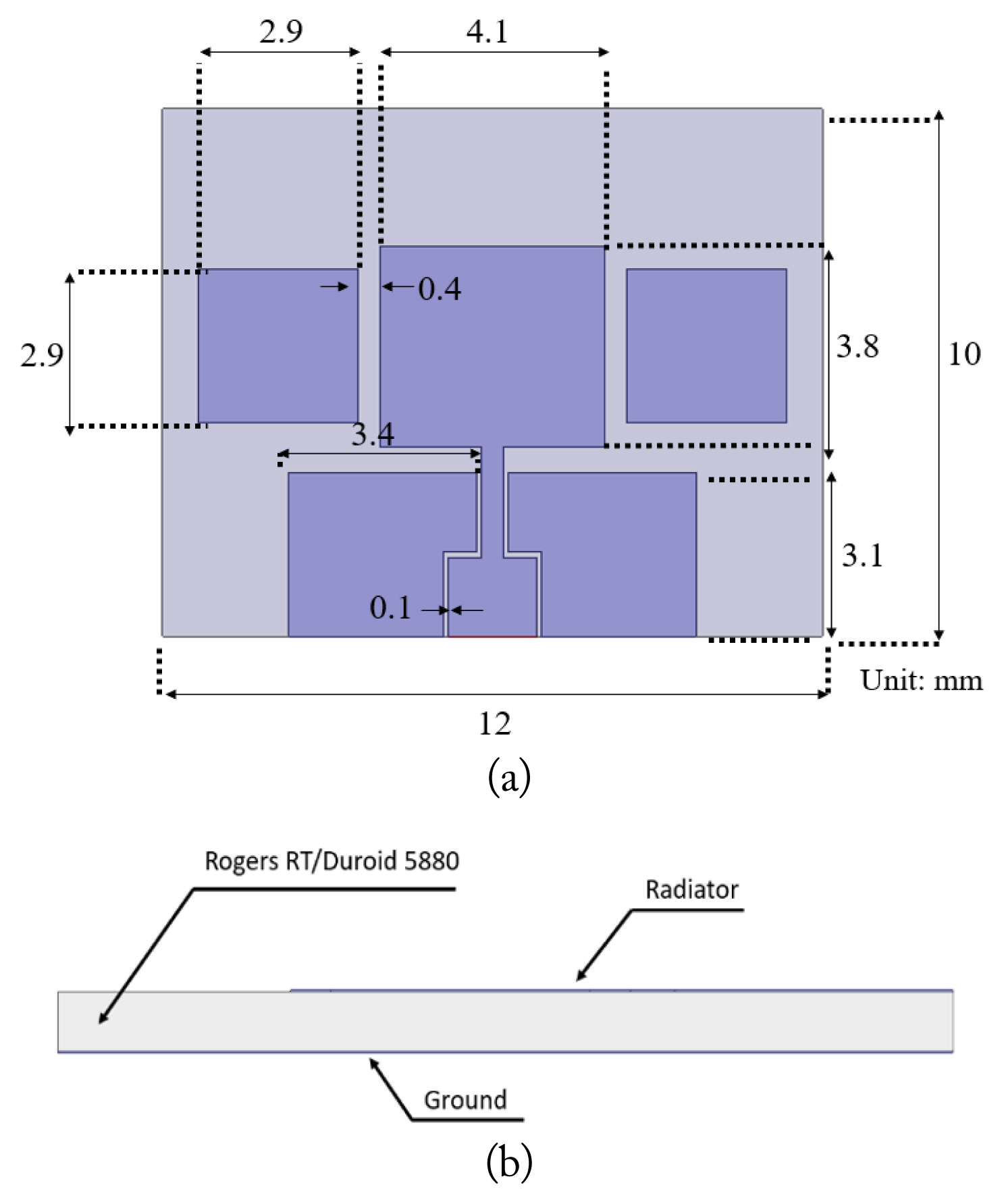
The overall structure of the proposed single microstrip patch antenna using parasitic elements fabricated on a Rogers RT/Duroid 5880 substrate (thickness = 0.508 mm) is shown in Fig. 1(a). Fig. 1(b) shows the side view of the proposed antenna. The overall dimensions are 12 mm ├Ś 10 mm, and it consists of one driven element and four parasitic elements. The driven element is matched with a quarter-wave transformer and the other parasitic elements are matched with the gap between the driving element and parasitic elements.
The impedance characteristic between the driven element and the parasitic element can be analyzed with even- and oddmode capacitance [10]. The even- and odd-mode capacitance can be defined by Eqs. (1) and (2). The impedance can be calculated by Eq. (3):
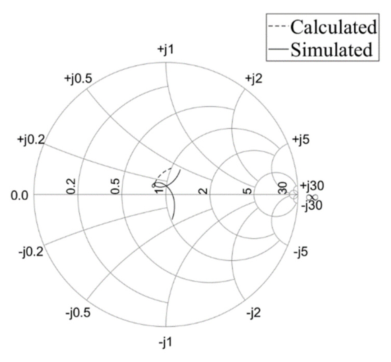
where Cp is the parallel plate capacitance between the driven element and the ground plane, Cf is the fringe capacitance, CfŌĆ▓ is the modified fringe capacitance due to the parasitic element, Cga is the gap capacitance, and Cgd is the capacitance that occurs due to the electric flux between the air and a dielectric. Based on this analysis, the input impedance was calculated. The results of the calculated and simulated input impedance at 24.25ŌĆō29.5 GHz are shown in Fig. 2. This figure shows that the calculated input impedance and the simulated input impedance do not perfectly match. However, the calculated input impedance based on the analysis provided in [10] helps to predict the simulated input impedance.
Fig. 3 shows the simulated current distribution on a single element. The first resonance at 24.8 GHz is due to the driven element (Fig. 2(a)), and the second and third resonances at 26.7 GHz and 28.7 GHz are due to the parasitic elements (Fig. 2(b) and 2(c)).
Fig. 4 shows the simulated E-field at each resonant frequency with a phase change of 90┬░. The distance between the proposed single antenna and the face on which the electric field is plotted is a quarter wavelength of each resonant frequency. It shows that the proposed single antenna is vertically polarized at each resonant frequency.
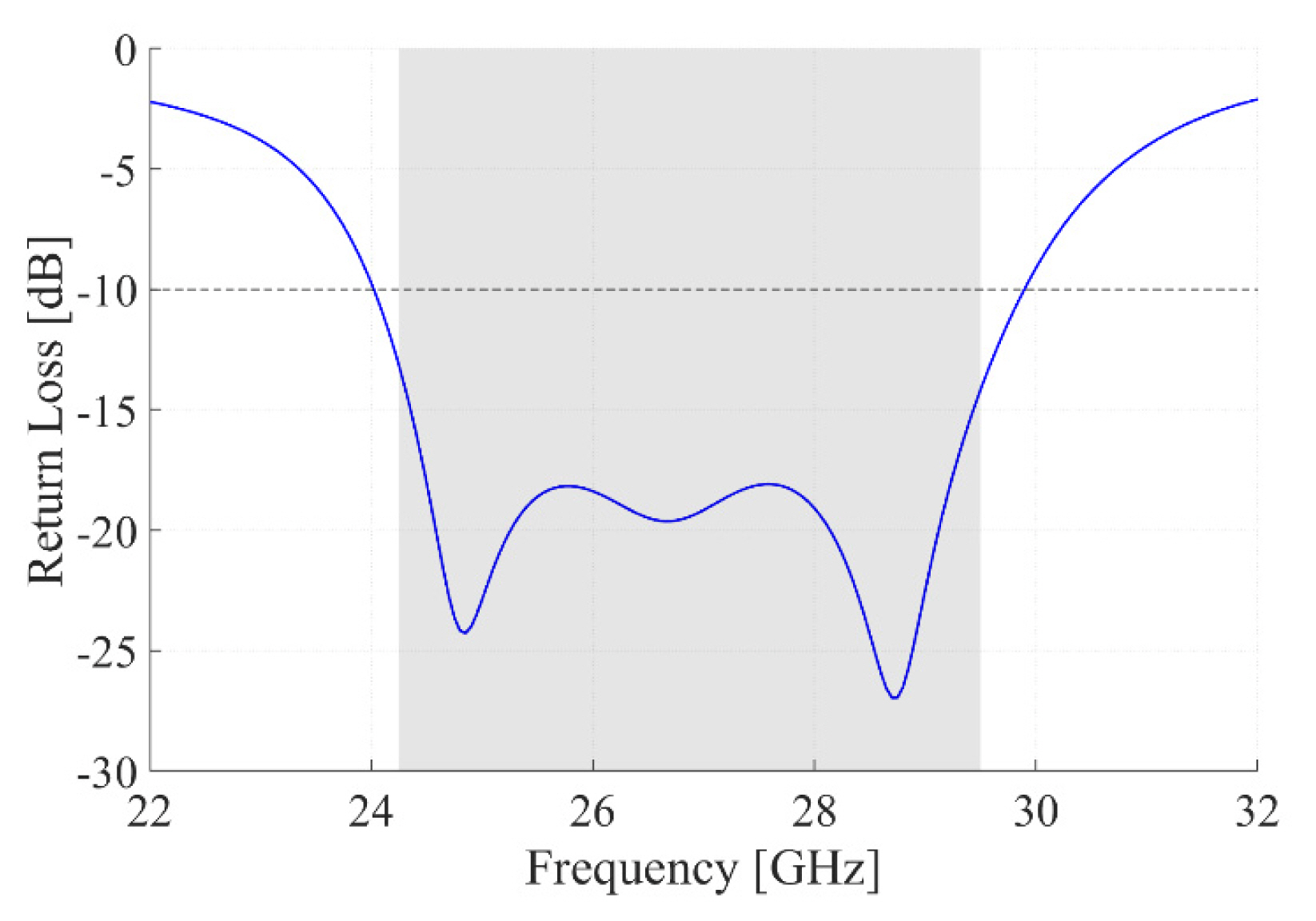
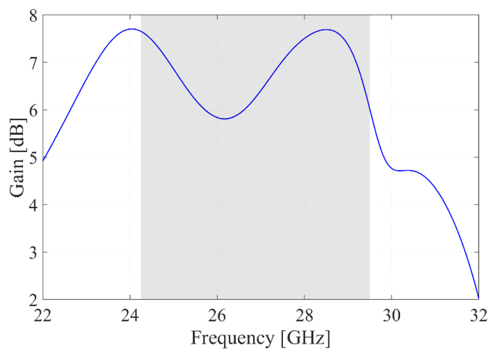
The simulated return loss (dB magnitude of S11) of the proposed single element is shown in Fig. 5. The proposed single element antenna achieved sufficient impedance bandwidth (dB magnitude of S11 < ŌłÆ10) of 24.2% (23.75ŌĆō30.3 GHz) to cover 5G NR n257, n258, and n261 bands (24.25ŌĆō29.5 GHz). Fig. 6 shows the simulated gain of the single element. It exhibits a minimum and maximum gain of 5.8 dB at 26.15 GHz and 7.69 dB at 28.55 GHz, respectively.
In an array antenna, feed networks are important. The feed loss, unwanted feed radiation, and wide feed impedance band must be considered when designing a feed network. In this feed network, multi-section or stepped transformers are used to achieve a wide impedance band [11, 12]. It is harder to match impedance in multi-section or stepped transformers than in a conventional feed network. Therefore, a detailed analysis of multi-section or stepped transformers is essential. Fig. 7 shows a detailed analysis of multi-section or stepped transformers.
The return loss of the microstrip line feed of multi-section or stepped transformers can be calculated by Eq. (4).
where SS is the S-parameter at the start of one stepped section and SE is the S-parameter at the end of one stepped section. ╬▓ is the propagation constant, and l is the length of one stepped section.
Since it uses a lot of multi-section or stepped transformers to achieve sufficient bandwidth, there are lots of discontinuous microstrip line parts in a feed network. The discontinuous and bent parts in a feed network cause electric charges to accelerate and result in unwanted radiation [13]. This unwanted radiation from the feed network destroys the array antennaŌĆÖs radiation pattern and reduces gain.
The cover, which is to be placed above the feed network, is proposed to prevent unwanted feed radiation and achieve high gain. To reduce the feed loss, the bent part of the feed is modified into a curve.
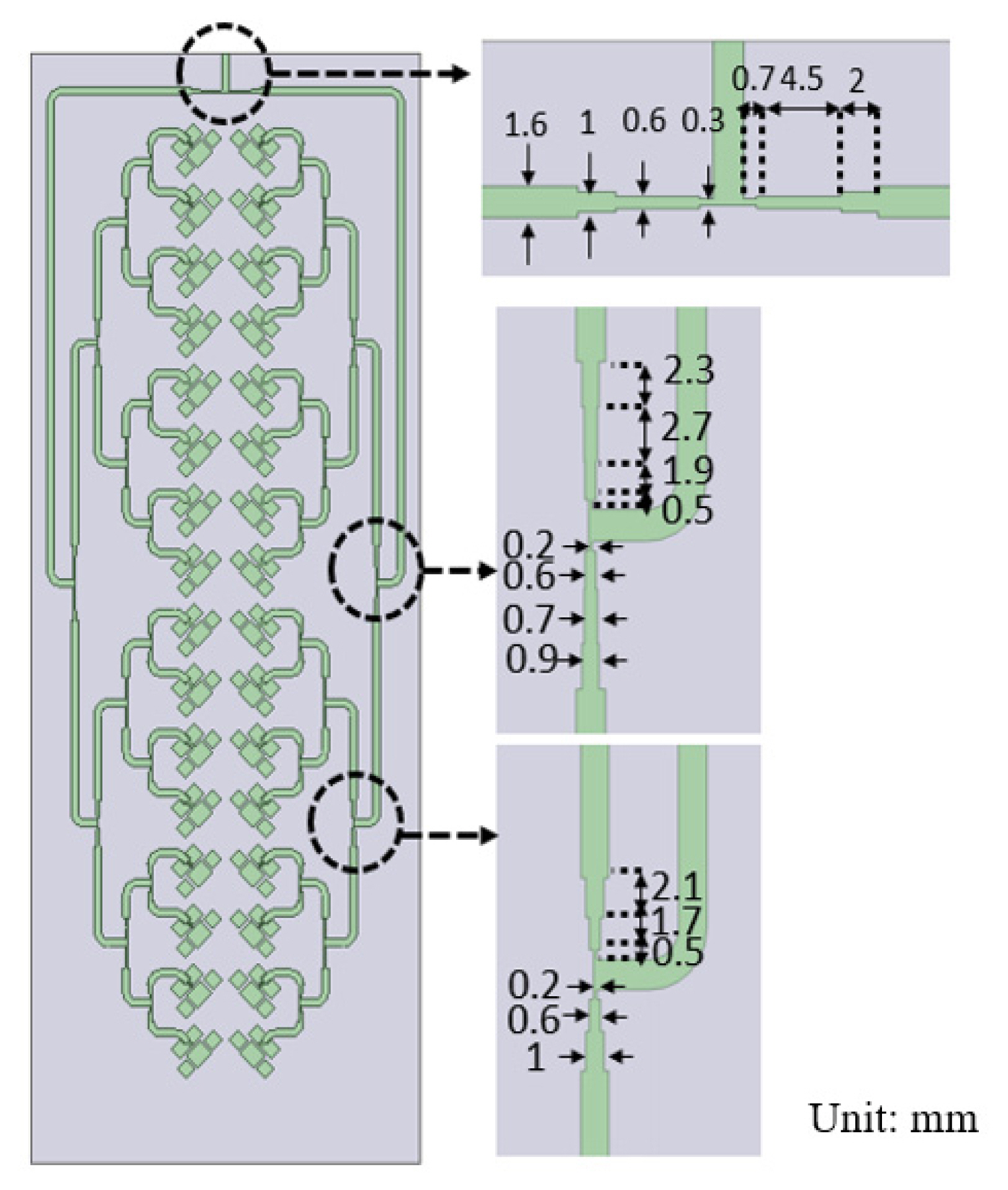
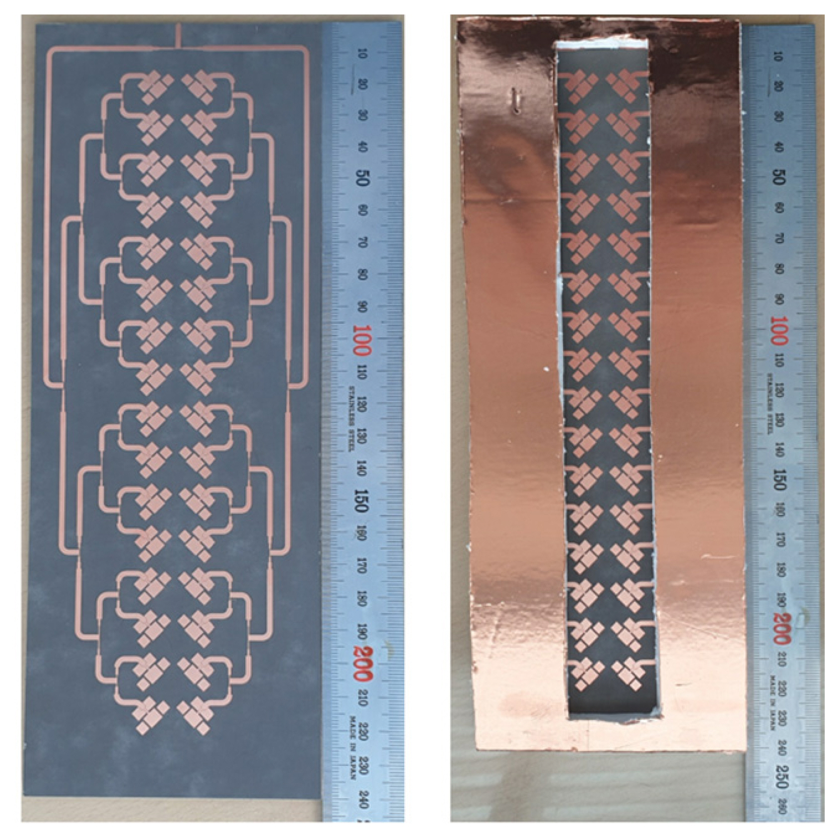
Fig. 8(a) shows the overall view of the 2 ├Ś 16 antenna with the feed network and cover. The radiators were tilted ┬▒45┬░ for orthogonal polarization. In the proposed array antenna, the space between elements is 3.8 mm (Ōēł ╬╗/2 at 28 GHz). The total size of the antenna is 90 mm ├Ś 240 mm. Fig. 8(b) shows the side view of the 2 ├Ś 16 antenna. The cover is located 4 mm above the Rogers RT/Duroid 5880 substrate. Fig. 9 shows a detailed view of the 2 ├Ś 16 array antenna feed network. Fig. 10 shows the prototype of proposed antenna.
III. Simulated and Measured Results
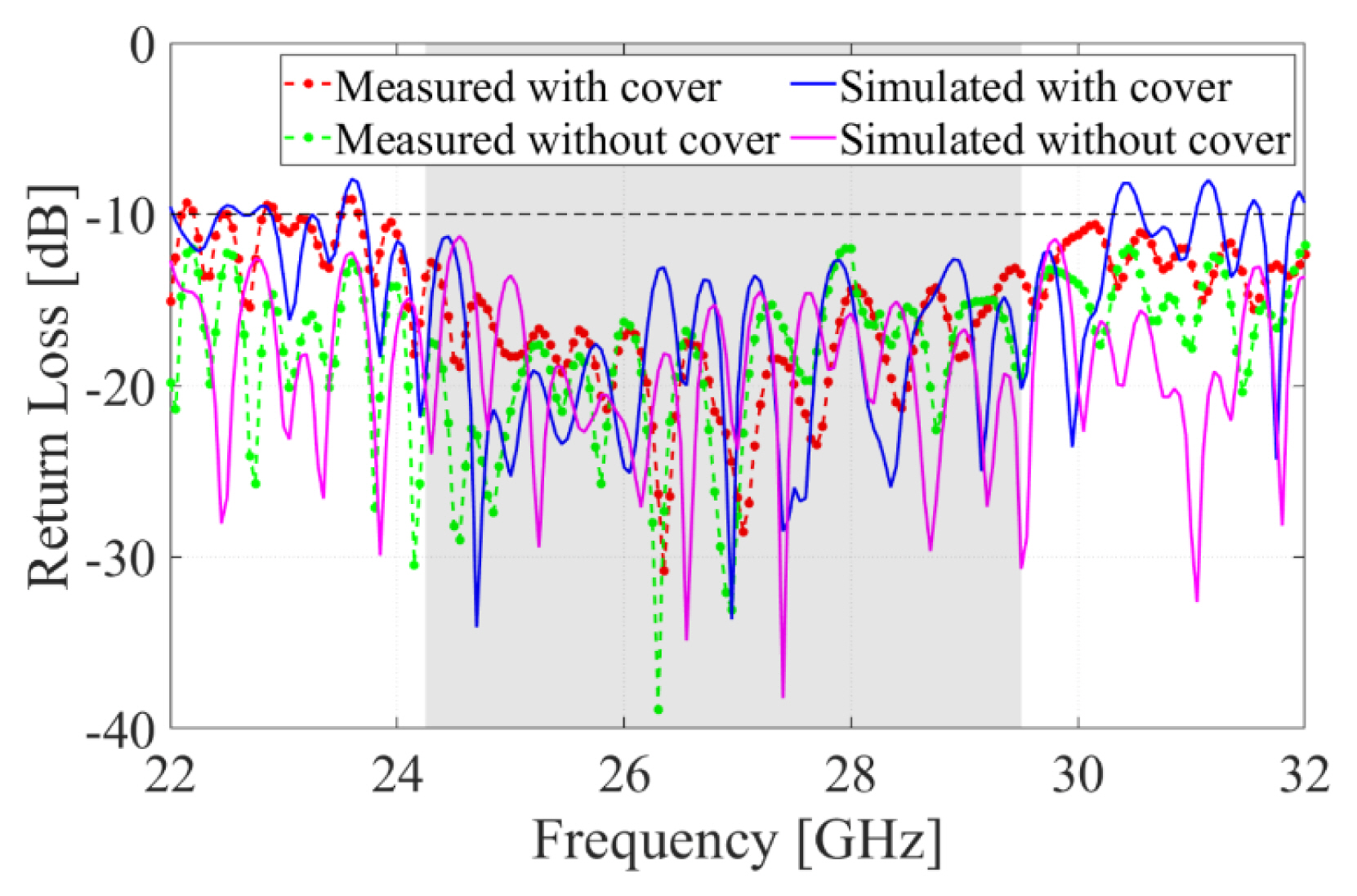
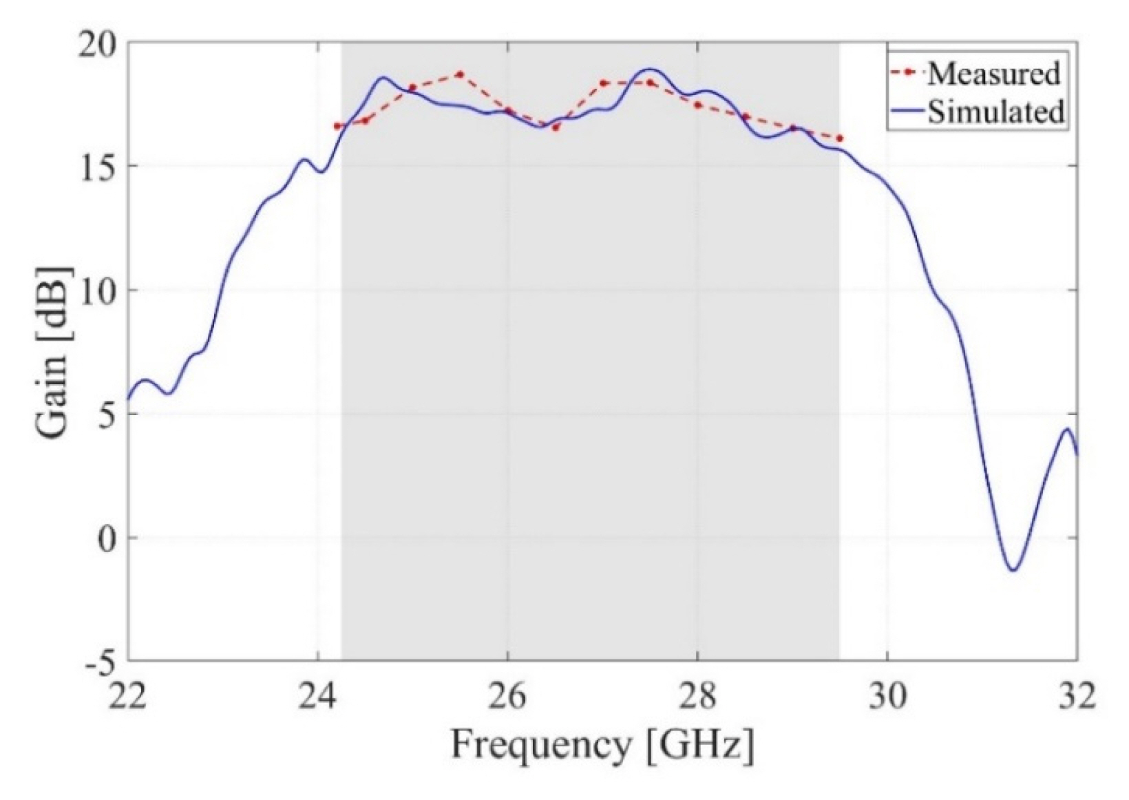
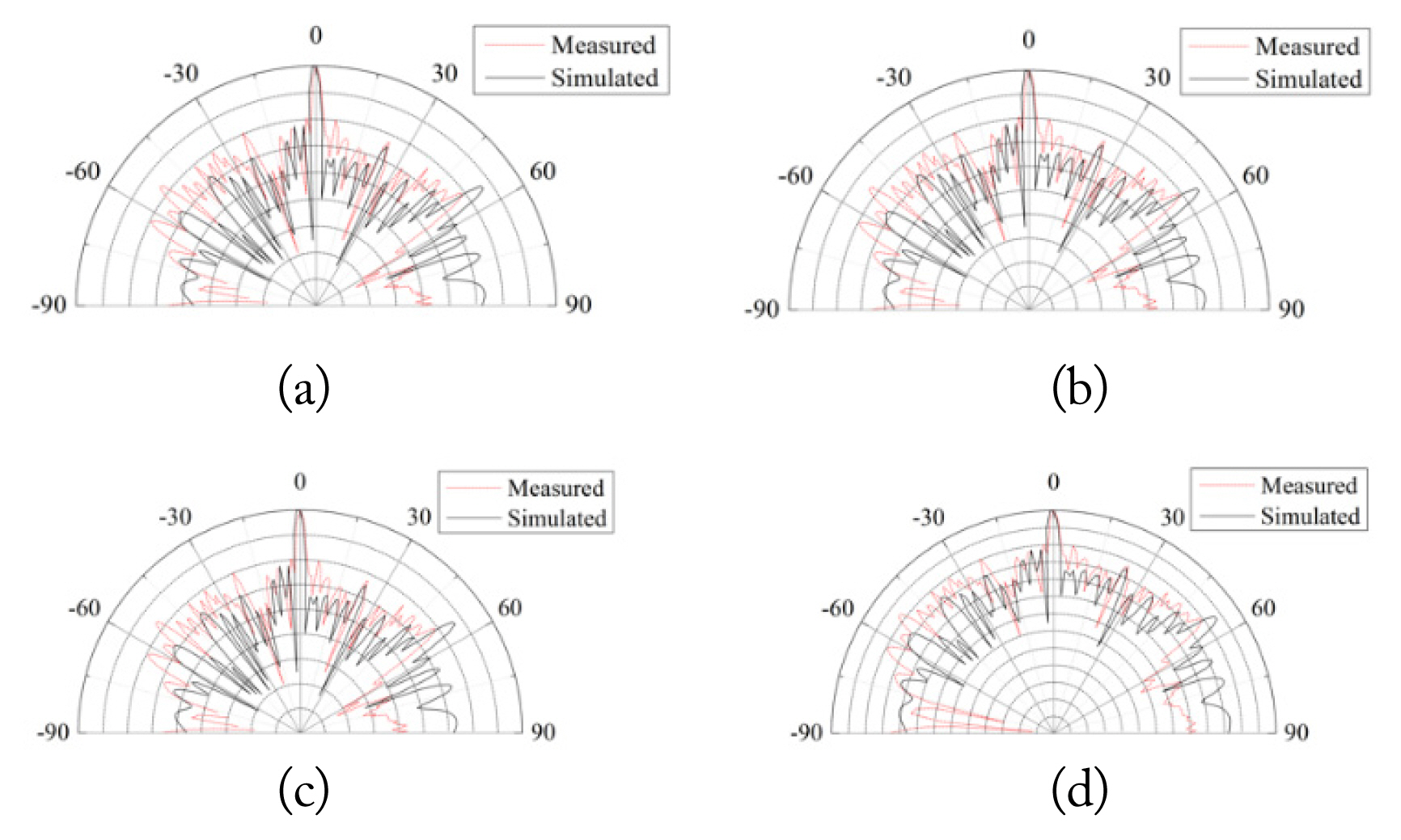
The simulated and measured return loss with and without covering (dB magnitude of S11) the proposed 2 ├Ś 16 element array is shown in Fig. 11. Many ripples are exhibited because of multi-section or stepped transformers and bent parts in the feed. Despite the many ripples, the return loss measurement result indicates that the proposed array antenna provides a sufficient impedance bandwidth of 29.8% (23.7ŌĆō32 GHz) when taking into account the 5G NR n257, n258, and n261 bands (24.25ŌĆō29.5 GHz). Fig. 12 shows the simulated and measured gain of the proposed array antenna. The proposed array antenna exhibits a peak measured gain of 18.69 dB at 25.5 GHz and a simulated peak gain of 19 dB at 27 GHz. The simulated and measured radiation patterns and the XPD of the proposed array antenna are shown in Figs. 13 and 14, respectively. The XPD can be calculated by Eq. (5):
The proposed array antenna exhibits a minimum and maximum measured XPD of 30.69 dB at 24.5 GHz and 46.7 dB at 27.5 GHz, respectively, whereas a minimum and maximum XPD of 32 dB at 25.95 GHz and 49 dB at 26.5 GHz were obtained in the simulated result.
IV. Conclusion
A wideband patch array antenna for 5G NR n257 (26.5ŌĆō29.5 GHz), n258 (24.25ŌĆō27.5 GHz), and n261 (27.5ŌĆō28.35 GHz) bands was proposed. The proposed antenna was fabricated on a single substrate to reduce manufacturing costs. Parasitic elements and an array antenna feed with multi-section or stepped transformers were used to achieve sufficient bandwidth to cover the 5G NR n257, n258, and n261 bands (24.25ŌĆō29.5 GHz). The radiators were tilted ┬▒45┬░ to achieve polarization diversity and high polarization discrimination while performing orthogonal dual polarization. A cover was proposed to prevent unwanted radiation from the feed line. Based on the measurements, the antenna supplied an impedance bandwidth (dB magnitude of S11 < ŌłÆ10) of 29.8% (23.7ŌĆō32 GHz). The measured peak gain was 18.69 dB. The measured gain was slightly lower than the simulated gain owing to the loss of the connector and the incorrect height of the feed cover. The measured XPD was higher than 30.69 dB. The proposed antenna presented was capable of covering the 5G NR n257, n258, and n261 bands (24.25ŌĆō29.5 GHz) and was found to be suitable for high-frequency 5G wireless communication.