A Millimeter-Wave GaN MMIC Front End Module with 5G NR Performance Verification
Article information
Abstract
This paper proposes a millimeter-wave (mmWave) 5G front end module (FEM) based on multiple gallium nitride (GaN) monolithic microwave integrated circuits (MMICs) with 5G new radio (NR) performance verification. The proposed structure is configured by a wide band GaN single-pole double-throw (SPDT) switch MMIC, a GaN low-noise amplifier (LNA) MMIC, and a GaN power amplifier (PA) MMIC with the target operation band from 26.5 GHz to 29.5 GHz. The LNA and PA MMICs are designed with 150 nm GaN/SiC technology, and the SPDT MMIC is designed with 100 nm GaN/Si. The LNA MMIC shows the measured noise figure less than or equal to 2.52 dB within the operation band. The PA MMIC is based on a two-stage configuration and shows about 35 dBm measured saturated power with power-added efficiency better than 34% within the operation band. Also, the SPDT MMIC is based on an artificial transmission line configuration for wideband performance and shows that the measured insertion loss is less than 1.6 dB, and the measured isolation is higher than 25 dB within the operation band. Furthermore, all MMICs are integrated within a single carrier as an FEM and successfully verified by 5G NR test signals.
I. Introduction
With the increasing demand for high-capacity, high-throughput and low-latency communication, the practical deployment of millimeter-wave (mmWave) 5G is being intensively investigated to leverage the full potential of next-generation communications. Since the transmitter and receiver core architecture must undergo radical innovations in the mmWave spectrum, the unprecedented challenges in the wave transmission and propagation efficiency in the mmWave band must be thoroughly considered. To meet the required specifications of mmWave-5G applications, the conventional circuit fabrications with CMOS or GaAs technologies are no longer sufficient in terms of both performance criteria and power efficiency. In particular, the critical limitation of a GaAs HEMT is its relatively low power density, resulting in unsatisfactory output power generation for high power request. Owing to the need for high-frequency high power amplifiers (PAs) and high-voltage devices in power electronics, the gallium nitride (GaN) technology has been rapidly growing with its capability in handling high power and continuous effort to reduce the fabrication cost.
Since the primary advantage of GaN HEMT technology is emphasized by its high-power capability, many mmWave GaN PA MMICs (monolithic microwave integrated circuits) on both silicon carbide (SiC) and silicon (Si) substrates have been previously reported [1–5]. Furthermore, with the emergence of the mmWave-5G market, high-performance and cost-effective multifunctional chips for both transmitter and receiver designs are in significant demand. Since GaN also provides good noise performance, GaN MMIC-based front end modules (FEMs) have been also proposed in different bands covering S-, C-, X-, and Ku-bands [6–10]. However, despite there being many individual GaN MMICs, there have been few existing studies on a complete Ka-band component including switch, PA, and LNA MMICs, as an integrated module. Moreover, there are few GaN MMIC FEMs with practical 5G new radio (NR) measurement and verification. Thus, in this paper, a mmWave FEM configured by a GaN/SiC PA, a GaN/SiC LNA, and a GaN/Si single-pole double-throw (SPDT) switch MMICs is designed for n257 band and verified with 5G NR test signals.
II. Design and Analysis
Fig. 1 shows the proposed FEM based on a multichip configuration including PA, LNA, and SPDT switch MMICs within a package. The proposed FEM MMICs are designed with two commercially available process technologies: WIN-semi 150 nm GaN/SiC for PA and LNA MMICs and OMMIC 100 nm GaN/Si for SPDT MMIC. The PA and LNA are designed with GaN/SiC to consider the power handling capability and efficiency, whereas SPDT is designed with GaN/Si to consider the cost-effectiveness. The process technology features are summarized in Table 1.

Configuration of the proposed FEM based on GaN PA, LNA, and switch MMICs.

Parameter summary of GaN HEMT processes
1. GaN/SiC LNA and PA MMIC Design
Fig. 2 shows the DC characteristics of the different GaN/SiC HEMT sizes with a gate-source voltage step for 0.1 V from −2.5 V to 0 V. With the drain voltage of 20 V and gate biasing voltage of −1.2 V, the simulated power density of 480 μm HEMT is found as 4.81 W/mm. Also, with the drain voltage of 5 V and gate biasing voltage of −1.5 V, the simulated power density of 100 μm HEMT is determined as 1.25 W/mm. Next, both HEMT devices are simulated to determine the optimized impedances for the maximum output power of PA and noise figure (NF) of LNA from 26.5 GHz to 29.5 GHz. Fig. 3(a) shows the simulated source and load impedances of 480 μm HEMT as a PA unit cell with drain voltage of 20 V and gate voltage of −1.2 V on the Smith chart at 28 GHz. The simulated source and load impedances of 0.84 + j1.21 Ω and 5.73 + j20.45 Ω, respectively are chosen to obtain the simulated maximum output power and PAE (power-added efficiency) of 32.4 dBm and 52.37%, respectively. In addition, Fig. 3(b) show the simulated source and load impedances of 100 μm HEMT as an LNA unit cell with drain voltage of 5V and gate voltage of −1.5 V on the Smith chart at 28 GHz. The simulated source and load impedances of 13.1 + j39.17 Ω and 31.23 + j19.74 Ω are chosen to obtain the simulated NF and available gain of 0.95 dB and 6.28 dB, respectively. Based on the source and load pull simulations from 26.5 GHz and 29.5 GHz, the obtainable output power, gain, and PAE for the PA unit cell, and NF, gain, and PAE for the LNA unit cell are summarized in Table 2.

DC characteristics of GaN/SiC HEMTs with (a) 480 μm and (b) 100 μm sizes.
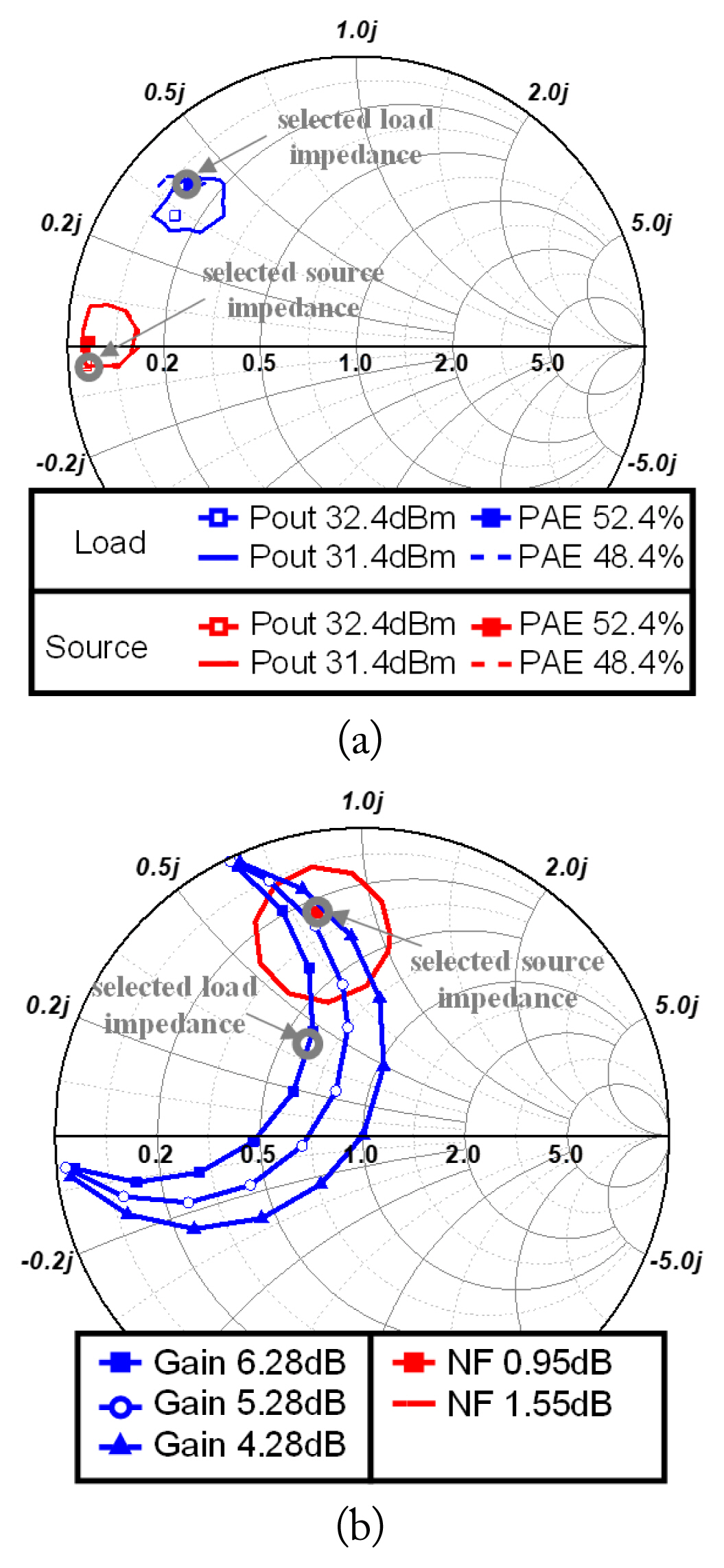
Source and load pull simulated impedances of (a) 480 μm and (b) 100 μm GaN/SiC HEMTs.

Simulated parameter summary of the HEMT cells
Using the selected 100 μm HEMT cells, a three-stage single-ended LNA is designed as shown in Fig. 4(a). The VDD and VGS for all stages are biased with 5 V and −1.5 V, respectively. Then, Fig. 4(b) shows the simulated S-parameters and NF of the designed LNA. The simulated minimum NF from 26.5 GHz to 29.5 GHz is about 1.62 dB, whereas the simulated minimum gain is about 20 dB. The gain variation is less than 1 dB within the operation band. In addition, Fig. 4(c) shows the simulated output P1dB from 26.5 GHz to 29.5 GHz. The minimum output P1dB of 10.5 dBm is observed at 29.5 GHz, while the output P1dB variation within the operation band is less than 1.5 dB.
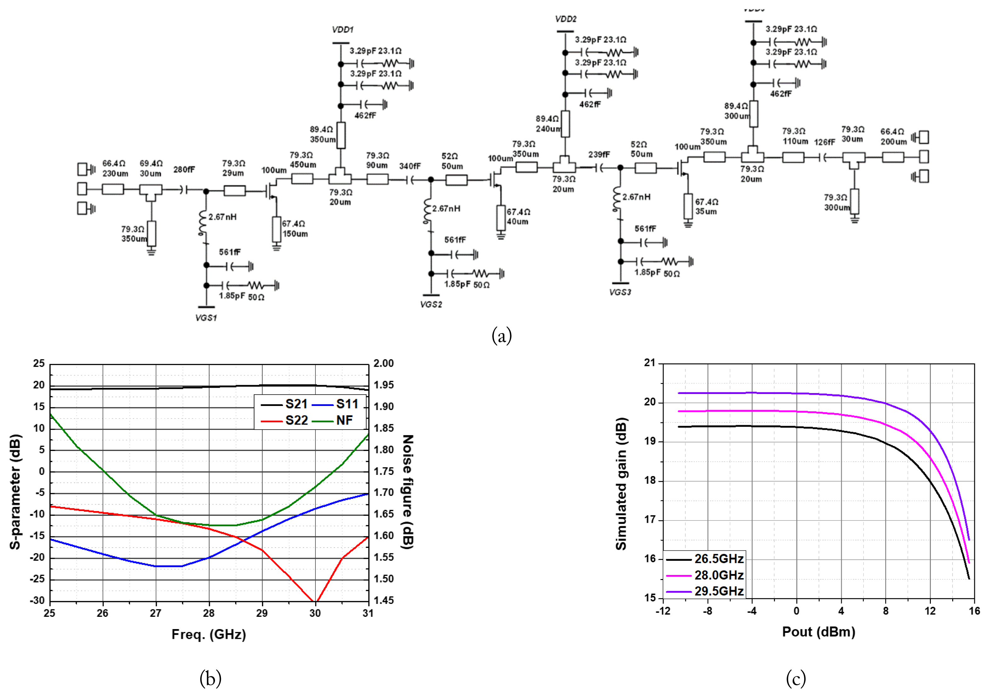
GaN/SiC LNA MMIC with (a) a design schematic and simulated (b) S-parameters and NF, and (c) gain and output P1dB.
Next, a two-stage PA is designed with the selected 480 μm HEMT devices, as shown in Fig. 5(a). The VDD and VGS in all stages are biased with 20 V and −1.2 V, respectively. In the second stage, two HEMT cells are used for parallel power combining to achieve the simulated output power of 35.4 dBm. Fig. 5(b) and 5(c) show the simulated S-parameters and output P1dB from 26.5 GHz to 29.5 GHz. The maximum gain of the PA is about 22.4 dB at 26.5 GHz and the gain variation within the operation band is less than 2.5 dB. Also, the simulated minimum output P1dB of 27 dBm is observed at 29.5 GHz, while the P1dB variation within the operation band is less than 3 dB. Furthermore, Fig. 5(d) shows the simulated PAE of the PA, and the maximum PAE of 31.5% is observed at 28 GHz.
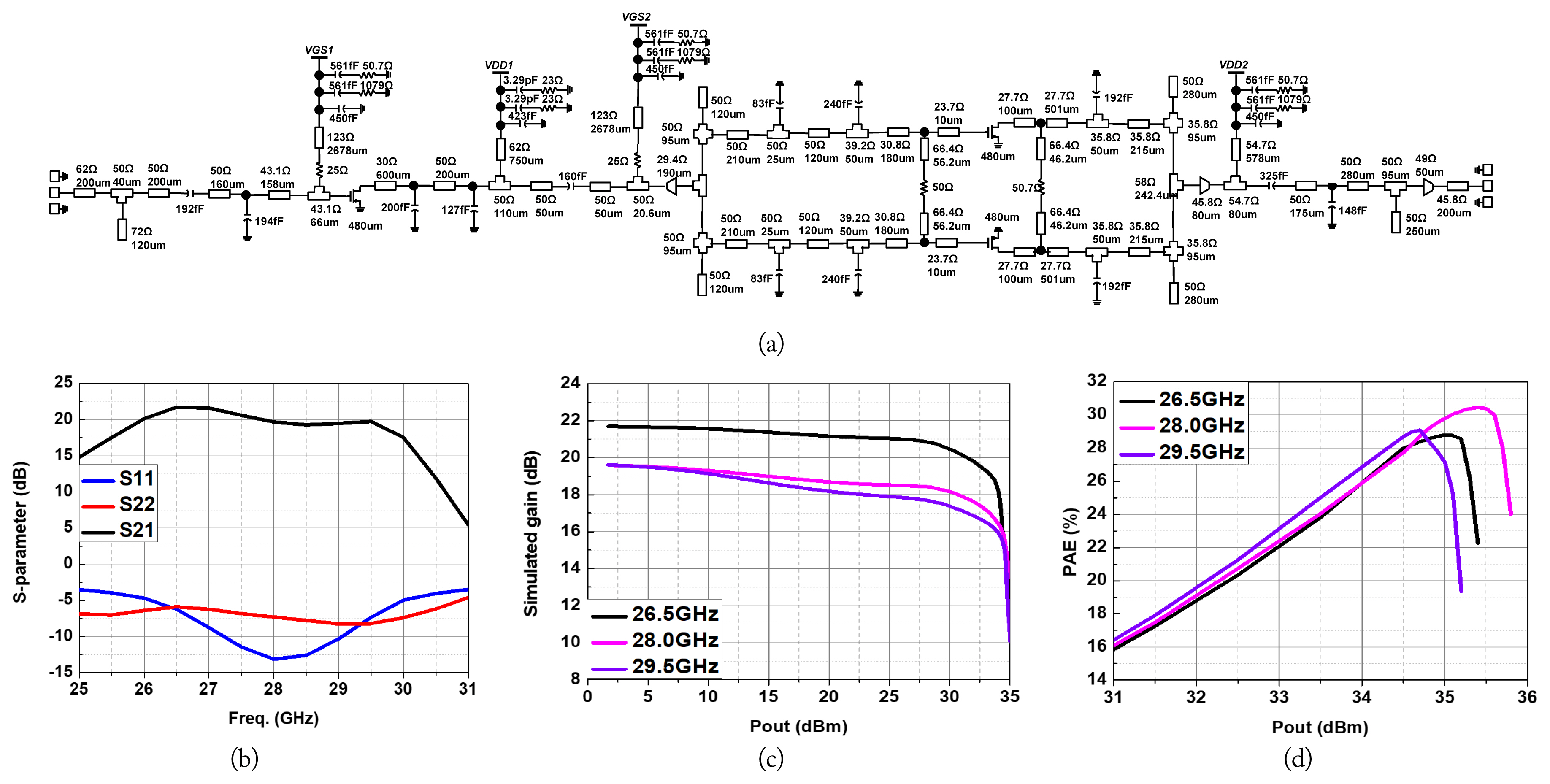
GaN/SiC PA MMIC with (a) a design schematic and simulated (b) S-parameters, (c) output P1dB, and (d) PAE.
2. GaN/Si SPDT Switch MMIC Design
Fig. 6(a) and 6(b) show the typical switch characteristics of the GaN/Si HEMT device having the size of 50 μm. As the operation frequency reaches the mmWave band, the parasitic reactance and resistive loss of the HEMT device increase drastically, resulting in poor ON-and-OFF performance. Thus, to ensure wideband operation and high isolation between the ON and OFF states, an artificial transmission line-based SPDT switch is designed, as shown in Fig. 7(a). The simulated S-parameters are shown in Fig. 7(b). Here, the simulated insertion loss is always less than 0.97 dB, while the simulated isolation is always better than 31.5 dB within the selected operation bandwidth from 26.5 GHz to 29.5 GHz. Furthermore, the simulated input P1dB of the SPDT within the operation band is more than 40 dBm.

GaN/Si HEMT switch characteristics with simulated (a) on and off state impedances and (b) S-parameters.

GaN/Si HEMT-based SPDT MMIC with (a) schematic design and (b) simulated S-parameters.
3. Bonding Wire with Transmission Line Matching
Since the proposed FEM is configured by multiple MMICs with bonding wire connections, the mismatch caused by the bonding wires must be considered. Thus, the printed circuit board (PCB) transmission lines with bonding wires are simulated as shown in Fig. 8(a). Specifically, the microstrip line with the bonding wire only is compared to the microstrip line with the boding wire compensated by a matching pad. In the simulation, a Taconic TLY-5 substrate with a relative permittivity of 2.2, loss tangent of 0.0009, and thickness of 2.54 mm is used. Then, Fig. 8(b) shows that the simulated insertion loss within the operation band is always better than 0.35 dB with the matching capacitive pad. Furthermore, the insertion loss fluctuation over the frequencies is improved by adopting the matching pad. According to Fig. 8(b), the simulated loss variation is less than 0.2 dB within the target operation band.
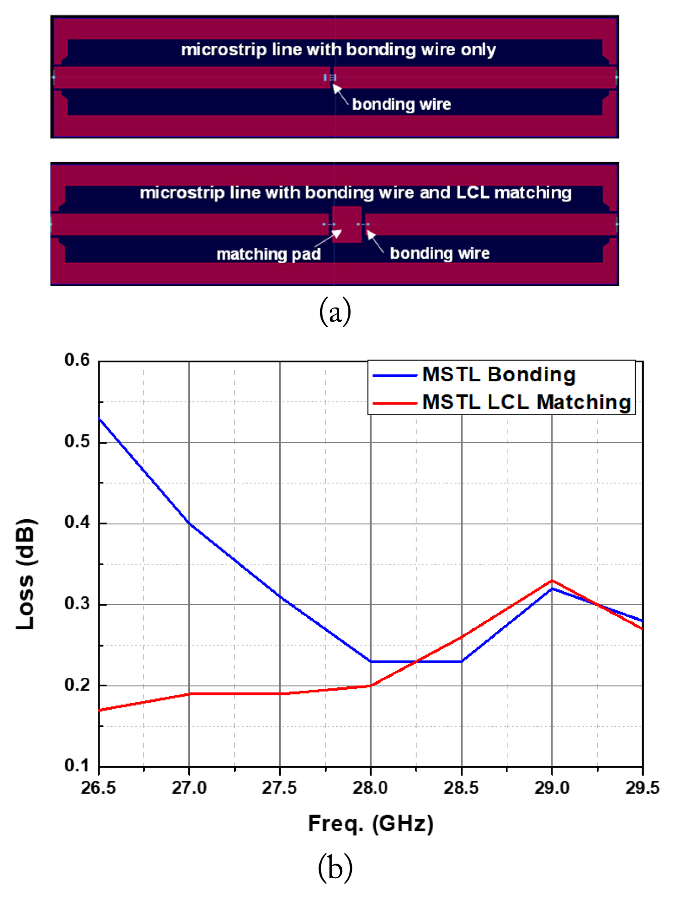
Analysis of the bonding wire by (a) microstrip transmission line (MSTL) with and without a matching pad, and (b) simulated S-parameters.
III. Fabrication and Measurement
1. Measurement of the Fabricated MMICs
The LNA and PA MMICs are fabricated with the WIN-semi 150 nm GaN/SiC process, as shown in Fig. 9(a) and 9(b), respectively. Also, the SPDT switch is fabricated with OMMIC 100 nm GaN/Si process, as shown in Fig. 9(c). The fabricated MMIC sizes of LNA, PA, and SPDT including bonding pads are 3.18 mm × 1.745 mm, 6.15 mm × 2.36 mm, and 1.16 mm × 2.35 mm, respectively. Then, Fig. 10(a) shows the measured S-parameters and NF of the fabricated LNA MMIC in comparison with the simulated results. The measured NF is 2.49 dB at 28 GHz, while the measured NF is always better than 2.52 dB from 26.5 GHz to 29.5 GHz. The measured 10-dB input and output impedance bandwidths are about 14.3% and 17.6%, respectively. Further, the measured gain is always better than 20 dB within the operation band. The measured output P1dB at 26.5 GHz, 28 GHz, and 29.5 GHz are 12 dBm, 12.6 dBm, and 12.6 dBm, respectively. Next, the simulated and measured S-parameters of the fabricated PA MMIC are shown in Fig. 11(a). The measured 10-dB input and output impedance bandwidths are about 8% and 19.6%, respectively, with the center frequency of 28 GHz. The measured gain within the operation band is always better than 15.7 dB, as well. Also, the measured output P1dB at 26.5 GHz, 28 GHz, and 29.5 GHz are 26.6 dBm, 26.6 dBm, and 26.7 dBm, respectively as shown in Fig. 11(b). Furthermore, the measured peak PAE at 26.5 GHz, 28 GHz, and 29.5 GHz are 35.47%, 34.93%, and 34.58%, respectively as shown in Fig. 11(c). The measured PAE is noted to be unusually higher than the simulated PAE. A mismatch is suspected between the simulation PDK model and real transistor model since we notice a difference between the simulated and measured drain currents. Specifically, the simulated drain currents are 544.7 mA, 545.5 mA, and 543.8 mA, whereas the measured drain currents are 343.2 mA, 349.8 mA, and 354.6 mA at 26.5 GHz, 28 GHz, and 29.5 GHz, respectively for the same output power. Consequently, the measured PAE is found to be higher than the simulated PAE. Finally, Fig. 12 shows the simulated and measured S-parameters of the fabricated SPDT switch MMIC as well as the input P1dB. The 10-dB impedance is satisfied over the operation band and the measured insertion loss is always better than 1.92 dB with a variation less than 1 dB. Also, the measured isolation is always better than 24.2 dB within the operation band.

Fabrication of (a) GaN/SiC LNA, (b) GaN/SiC PA, and (c) GaN/Si SPDT switch MMICs.
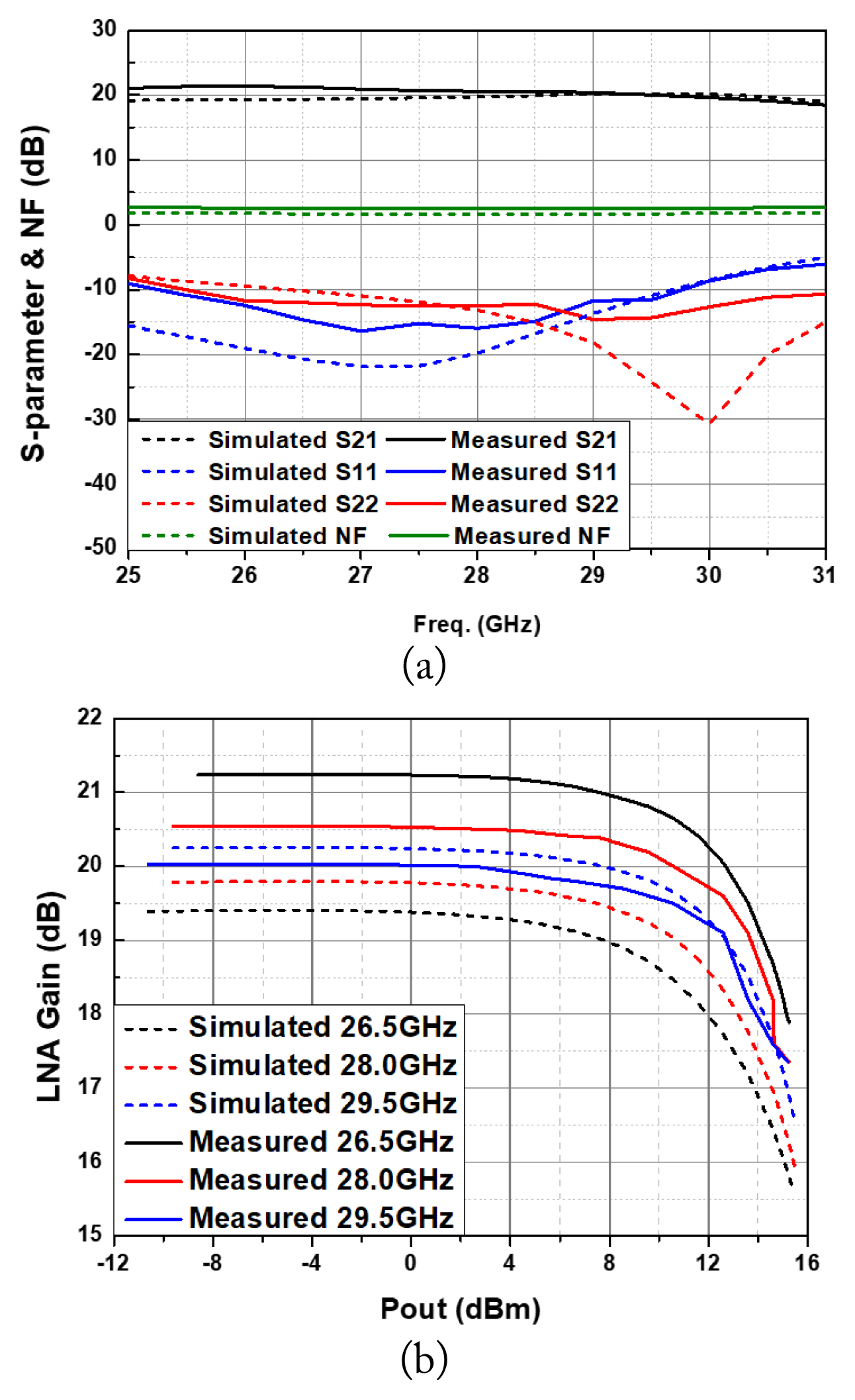
Simulated and measured (a) S-parameters and NF, and (b) gain and output P1dB of the fabricated GaN/SiC LNA MMIC.
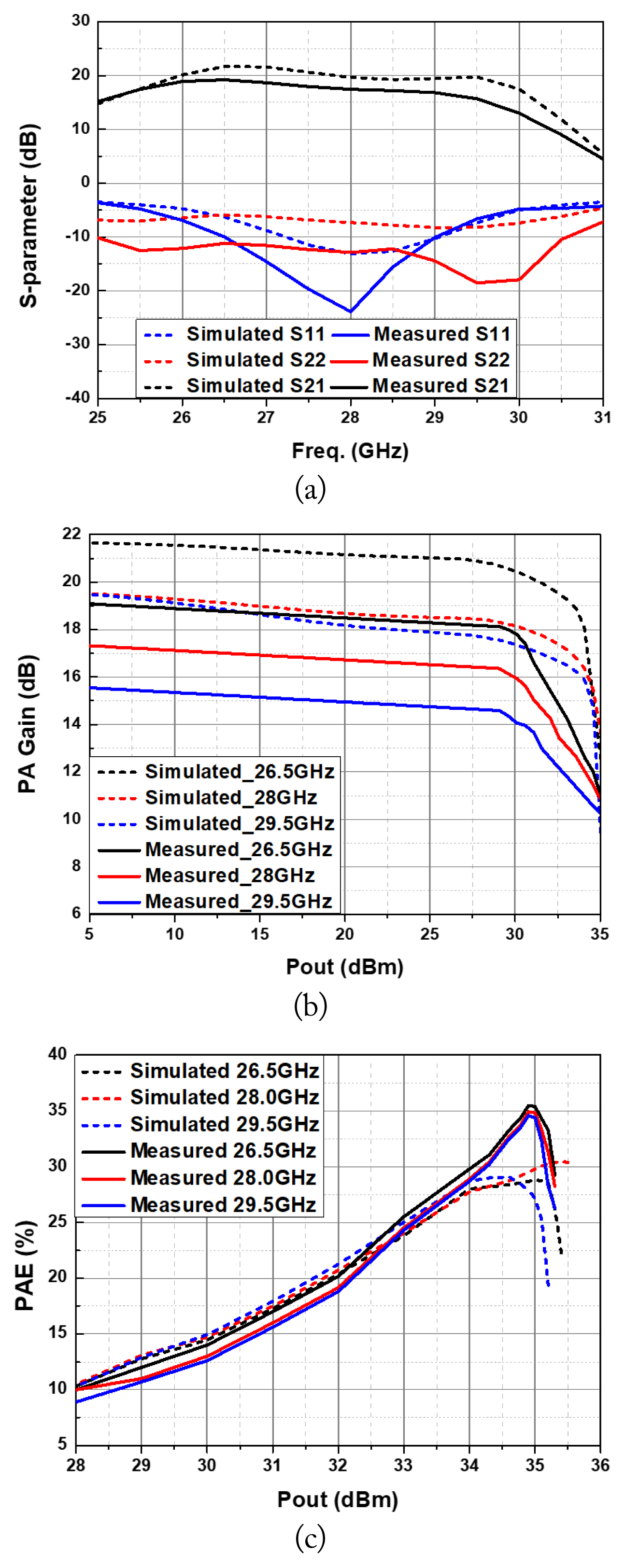
Simulated and measured (a) S-parameters, (b) output P1dB, and (c) PAE of the fabricated GaN/SiC PA MMIC.
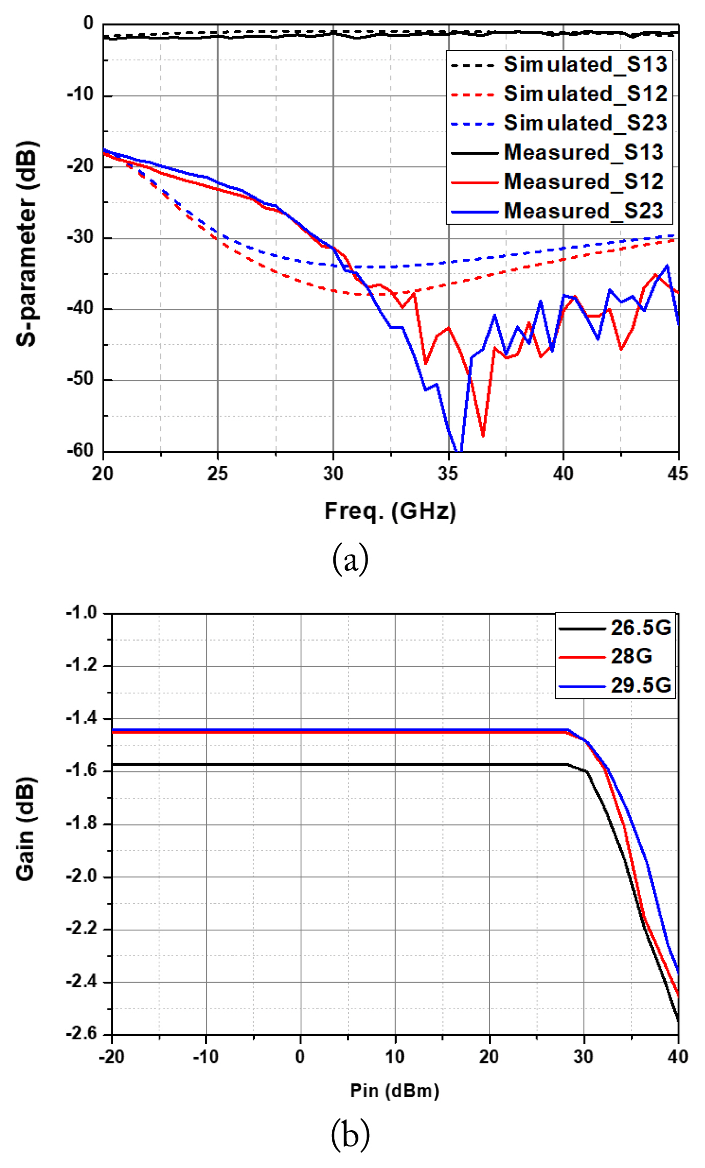
Fabricated GaN/Si SPDT switch MMIC with (a) simulated and measured S-parameters and (b) measured input P1dB.
Furthermore, the measured input P1dB is more than 40 dBm, resulting in a sufficient margin for handling PA output power in the target FEM.
2. Implementation and Measurement of the FEM
Before integrating the fabricated GaN MMICs as a single FEM, the conventional transmission lines and the lines with bonding wires are fabricated to verify the interstage line characteristics, as shown in Fig. 13. Each line is fabricated with the TLY-5 substrate identical with the simulation. The microstrip line with the matching pad shows the stable insertion loss within the operation band. The length of the bond wire is 0.35 mm. Further, the dimensions of the matching pad and 50 Ω line are 1.02 × 1.2 mm2 and 0.72 mm, respectively. Then, the complete FEM is implemented using the fabricated MMICs and interstage matching lines on a Taconic TLY-5 PCB and a 1.0-mm CPC (Cu-MoCu-Cu) heatsink carrier, as shown in Fig. 14(a). To verify the performance of the complete FEM, both Rx-mode and Tx-mode S-parameters are also measured, as shown in Fig. 14(b) and 14(c), respectively. For the Rx mode measurement, 5 V and −1.55 V are applied to VDD and VGS. According to Fig. 14(b), the measured minimum input and output reflection coefficients are about −8.8 dB and −9.9 dB from 26.5 GHz to 29.5 GHz, respectively, in the FEM Rx-mode. The measured small signal gain at 28 GHz is 15.8 dB, while the measured gain variation within the operation band is less than 14 dB. Also, the measured NF within the operation band is always better than 5.47 dB. Next, for the Tx mode measurement, 22.5 V, and −1.5 V and −1.8 V are applied to VDD and each VGS, respectively. The measured minimum input and output reflection coefficients in the FEM Tx-mode are about −4.42 dB and −4.4 dB, respectively, within the operation band, as shown in Fig. 14(c). The measured small signal gain at 28 GHz is 13.07 dB, while the measured gain variation within the operation band is less than 6.4 dB. Finally, the fabricated FEM in the Tx mode is verified with 5G NR 16 QAM and 100 MHz bandwidth test signals as shown in Fig. 15. The measured output powers are 20.18 dBm, 21.03 dBm, and 21.06 dBm, whereas the measured PAEs are 3%, 3.3%, and 2.8% at 26.5 GHz, 28 GHz, and 29.5 GHz, respectively. Furthermore, the measured EVMs are 4.65%, 4.78%, and 4.14% at 26.5 GHz, 28 GHz, and 29.5 GHz, respectively.
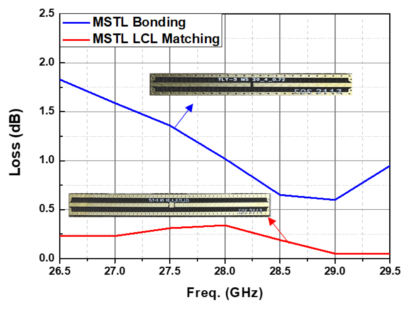
Measured insertion loss of interstage lines.
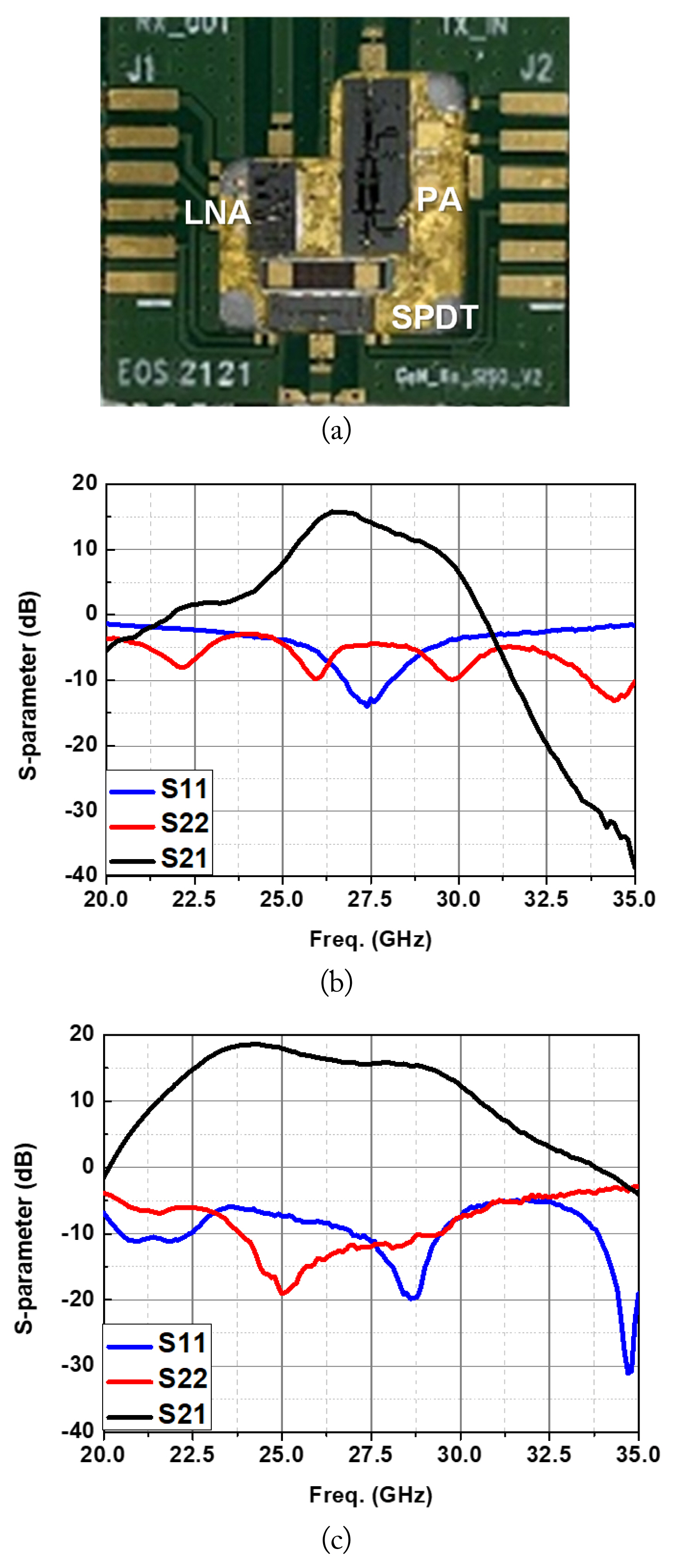
Fabricated FEM with (a) a photograph and measured S-parameters in (b) Rx-mode and (c) Tx-mode.

A 5G NR test with the proposed FEM Tx: (a) EVM test and (b) ACPR test.
IV. Conclusion
In this paper, the mmWave-5G FEM configured by GaN/ SiC LNA and PA MMICs, as well as a GaN/Si SPDT switch MMIC, is presented. Each MMIC is fabricated individually and shows a good agreement between the simulation and measurement. Then, all MMICs are integrated within a single carrier as an FEM and successfully verified by a 5G NR signal with 16-QAM, 100 MHz bandwidth, and 120 kHz source carrier spacing.
Acknowledgments
This work was supported in part by the Development of Civil Military Technology program (No. 21-CM-RA-02) from the Institute of Civil Military Technology Cooperation (ICMTC), and in part by the Korea Institute for Advancement of Technology (KIAT) grant funded by the Korea government (MOTIE) (No. P0017011, HRD Program for Industrial Innovation), and in part by the Chung-Ang University Research Scholarship Grants in 2020.
References
Biography

Ji-Hye Hwang received the B.S. degree in electronics engineering from Hanseo University, Seosan, South Korea, in 2018, and the M.S. degree in electronics and electrical engineering from Chung-Ang University, Seoul, South Korea, in 2021, respectively. Since 2017, she has been a research engineer in ICT Device & Packaging research center at Korea Electronics Technology Institute. Her research interests include RF circuits and communication systems, power amplifier module (PAM), RFIC/ MMIC, and front-end module (FEM).

Jiho Lee received the B.S. degree from Korea Aerospace University (KAU), Goyang, South Korea, in 2020. He is currently pursuing the M.S. degree in electrical and electronics engineering at Chung-Ang University, Seoul, South Korea. His research interests include mm-Wave antennas, and RF circuits.

Ki-Jin Kim received the B.S. degree in electrical engineering from Kookmin University, Seoul, South Korea, in 2003 and M.S. and Ph.D. degrees in electrical engineering from KAIST, Daejeon, South Korea, in 2006, 2013, respectively. From 2006 to 2018, he was a senior researcher and now he is a team leader in ICT device packaging center at Korea Electronics Technology Institute (KETI). His research interests include CMOS RF circuits, compound semiconductor MMIC, and modeling of the RF transistors.

Han Lim Lee received the B.A.Sc. degree in electronics engineering from Simon Fraser University, BC, Canada, in 2008 and the M.S. and Ph.D. degrees in electrical engineering from KAIST, Daejeon, South Korea, in 2010, and 2014, respectively. From 2014 to 2015, he was a senior engineer in DMC research center at Samsung Electronics. In 2015, he joined the school of electrical and electronics engineering in Chung-Ang University, where he is currently an associate professor. His research interests include RF circuits and communication systems, mmWave beam-forming antennas and phased array systems, antenna-in-package, RFIC/MMIC, scalable-RF module, and microwave wireless power transmission (MWPT).