J. Electromagn. Eng. Sci Search

CLOSE


J. Electromagn. Eng. Sci > Volume 22(6); 2022 > Article
Chaudhary and Jeong: A Tunable Bandpass Filter with Arbitrarily Terminated Port Impedance Using Dual-Mode Resonator

Abstract

This paper presents a design for a compact arbitrarily terminated port impedance tunable bandpass filter (BPF) with transmission zeros (TZs) that employs a dual-mode resonator. The proposed dual-mode resonator comprises two varactors along with series transmission lines and a shunt short-circuited stub. The resonant frequency separation of the dual-mode resonator can be adjusted by changing the length or characteristic impedance of the short-circuited stub. To achieve arbitrarily terminated port impedances, the coupling between the source/load and the dual-resonator is modified from the originally designed 50-to-50 Ω termination filter. Frequency selective characteristics are achieved by generating two TZs at the lower and upper frequencies of the passband. The location of the TZs can be changed by controlling the source-load coupling. To experimentally validate the proposed tunable BPF, three prototypes (50-to-50 Ω BPF, 25-to-50 Ω BPF, and 20 + j10-to-50 Ω BPFs) are designed and fabricated. The measurement results revealed that the center frequency can be tuned from 2.10 GHz to 3.02 GHz (920 MHz tunability), where the insertion loss varies from 1.50 to 2.5 dB.

I. Introduction

Microwave/millimeter wave bandpass filters (BPFs) with multifunctional capabilities are highly desirable for their potential to reduce circuit size and reduce the cost of next-generation wireless communication systems [1, 2]. So far, many designs have been proposed for tunable BPFs that employ different tuning elements such as varactor diodes, RF microelectromechanical systems (MEMS), or PIN diodes [35]. Among these, varactor-diode based planar tunable BPFs are of particular interest for their ease of easy integration into microwave communication systems. Previous studies have proposed various planar tunable BPF designs, each with a different topology and functionality, including bandpass to bandstop switchable, multi-band, and bandwidth (BW) control [613]. A planar tunable BPF that used a switched varactor diode resonator over a wide frequency tuning range (FTR) was presented in [14], however, this BPF had poor frequency selectivity characteristics. In [15], a two-pole tunable BPF was presented over a wide FTR, however, this design required numerous tuning elements and dc-bias voltage control elements.
Recently, tunable BPFs based on multi-mode resonators have attracted attention for their potential to reduce circuit size [1619]. In [20], a tunable BPF based on a synchronously tuned dual-mode resonator was tested. In addition, an electronically tunable planar BPF using a nonuniform Q-factor of dual-mode resonators was presented in [21] to enhance passband flatness. In [22], a wideband tunable BPF was designed with a multi-mode step-impedance resonator (SIR), however, this design exhibited poor frequency selectivity characteristics. Similarly, a second-order quasi-elliptic tunable BPF with a constant 3-dB BW using varactor-tuned dual-mode resonators was presented in [23]. In [24], a tunable BPF based on an element-variable coupling matrix and dual-mode resonators was demonstrated; however, this design required numerous tuning elements and a dc-bias control voltage element. The wideband tunable BPF based on a tunable external Q-factor and the multi-mode resonators presented in [25] also suffered same issues. In [26], a tunable BPF with a single dc-bias control was presented; however, this design exhibited high insertion loss and poor frequency selectivity characteristics.
In recent years, various BPFs with arbitrarily terminated port impedances have been reported [2730]. However, these arbitrarily terminated port impedances BPFs were reported at a fixed center frequency. Meanwhile, conventional tunable BPFs are limited to a 50-to-50 Ω (RS = RL = 50 Ω) termination impedance design. Thus, designing a frequency-selective BPF capable of center frequency tuning and arbitrary termination impedance is an important step in the miniaturization of emerging next-generation wireless communication systems.
This paper proposes a frequency selective tunable BPF with arbitrarily terminated port impedances based on a dual-mode tunable resonator. In this design, frequency selectivity is achieved by generating transmission zeros (TZs) located at the lower and upper frequencies of the passband. The proposed dual-mode tunable BPF with arbitrary port termination impedance is designed by modifying the coupling matrix of a 50-to-50 Ω frequency-fixed filter.

II. Design Method

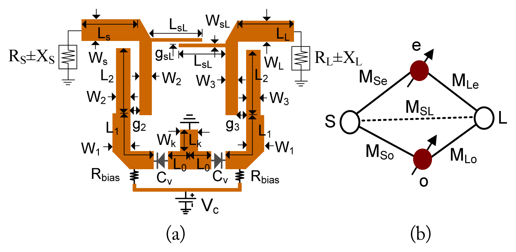
Fig. 1(a) depicts the proposed structure of a tunable BPF where the source and load ports are arbitrarily terminated with RS ± jXS and RL ± jXL impedances, respectively. The proposed tunable BPF comprises a dual-mode resonator that provides the even- and odd-mode resonant frequencies. Fig. 1(b) presents the coupling diagram of the proposed BPF, where each node represents even-and odd-mode resonant frequencies. In this figure, the solid and dashed lines illustrate the direct coupling and cross-coupling paths, respectively. Using a lossless (N + 2) × (N + 2) filter model, the coupling matrix of the proposed tunable BPF is given as (1), where the source and load ports are normalized to 1 Ω.
(1)
[M]=[0MSeMSoMSLMSeMee+x0MLeMSo0Moo+xMLoMSLMLeMLo0].
The diagonal elements of the coupling matrix have nonzero values, which represent the susceptance of a dual-mode resonator. The self-resonant frequencies (fe, even-mode; fo, odd-mode) of a dual-mode resonator can be calculated by as follows:
(2)
fe/o=fc2(4+(Mee/oo+x)2Δ2-(Mee/oo+x)Δ),
where fc, Δ, and x indicate the center frequency, fractional BW, and tuning element of the filter, respectively.
For a tunable BPF with a normalized arbitrary source impedance (rS±jxs) and load impedance (rL ± jxL), the (N + 2) × (N + 2) coupling matrix of filter is evaluated as follows:
(3)
[Mnew]=[0MSeMSoMSLMSeMee+x0MLeMSo0Moo+xMLoMSLMLeMLo0],
where
(4a)
MSe=MSers-xsrsMSe2,MSo=MSors+xsrsMSo2
(4b)
MLe=MLerL+xLrLMLe2,MLo=MLorL+xLrLMLo2
(4c)
Mee=Mee-xsrsMSe2,Moo=Moo-xsrsMSe2
(4d)
MSL=MSLrsrL,rs=Rs50,xs=Xs50,rL=RL50,xL=XL50
Similarly, RS and RL are the real parts and XS and XL are the imaginary parts of the source and load port impedances, respectively, which are normalized with reference to 50 Ω. The S-parameters of an arbitrary impedance terminated BPF can be obtained as.
(5)
S11=1+2jrS[A-1]1,1,S21=-2jrSrL[A-1]N+2,1,
where
(6a)
[A]=[Mnew-jR+ωW]
(6b)
ω=(ffc-fcf)Δ
[R] is the (N + 2) × (N + 2) is zero matrix, except for the non-zeros entries of R11=1/rs and RN+2,N+2=1/rL. Similarly, [W] is the (N + 2) × (N + 2) identity matrix except for W11=0 and WN+2,N+2=0.
Let us consider a case in which fc and Δ are 2.50 GHz and 4.40%, respectively, for a Chebyshev filter with a ripple of 0.043 dB. The synthesized (N + 2) × (N + 2) coupling matrix of the proposed tunable BPF with source and load ports of 1 Ω can be determined as.
(7)
[M]=[0-0.85970.81460.0630-0.85971.6619+x00.85970.81460-1.6675+x0.81460.06300.85970.81460].
The (N + 2) × (N + 2) coupling matrix of the arbitrarily terminated BPF can be calculated using (3) and (7).
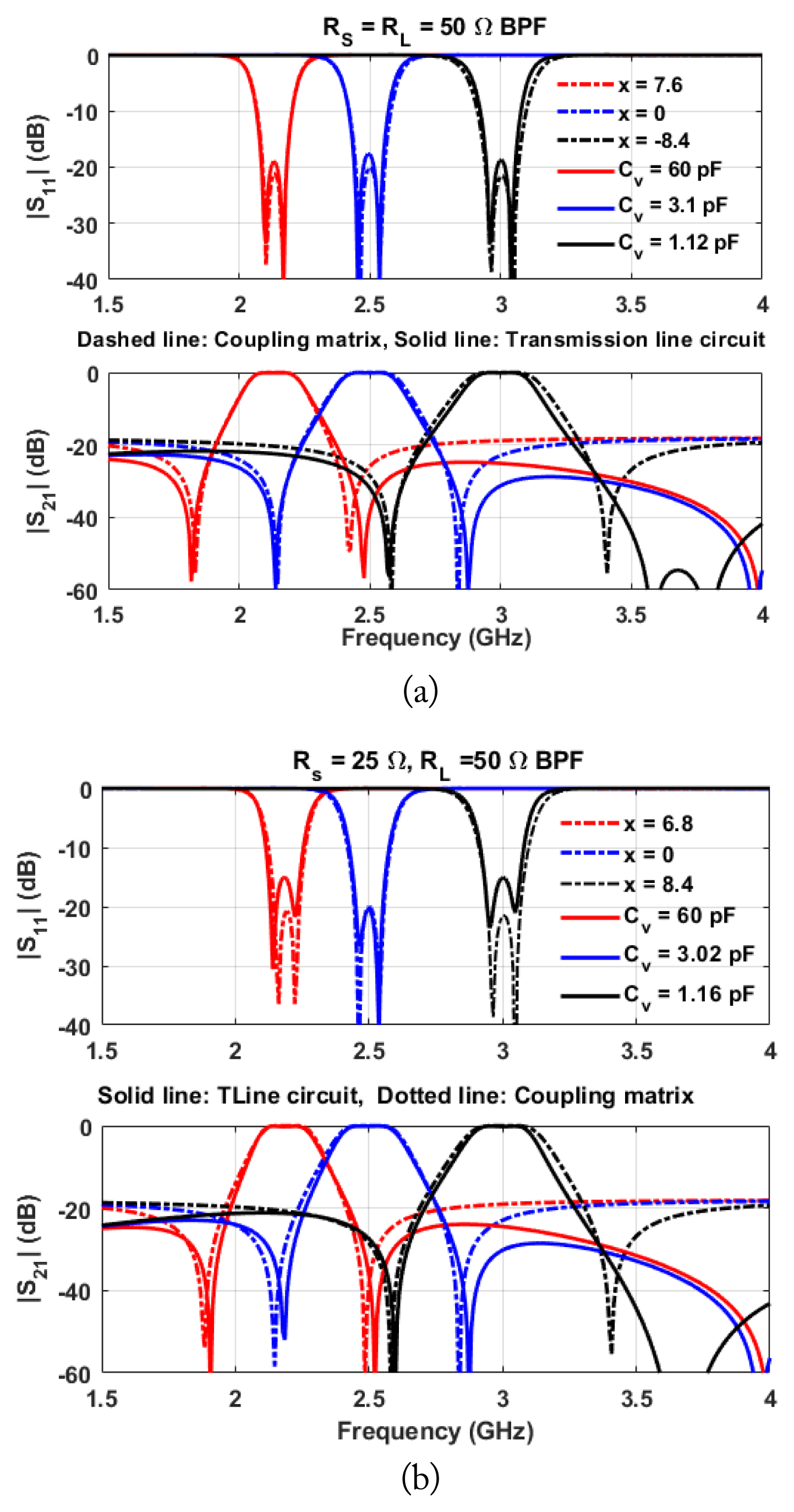
Fig. 2 shows the synthesis result of a tunable BPFs using a coupling matrix. The center frequency is tuned from 2.10 GHz to 3 GHz by varying x from −8.2 to 8.2. The TZs are located at the lower and higher frequencies of the passband. The location of the TZs can be controlled by changing the source-load coupling (MSL). Similarly, the TZs are also moved while tuning the center frequencies. These results indicated that even though the source and load termination impedances (RS and RL) of BPF are chosen arbitrarily, the response remans identical.

1. Proposed Dual-Mode Resonator

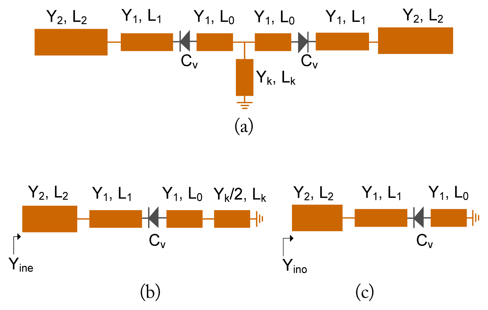
Fig. 3 shows the structure of the proposed dual-mode resonator, which comprises of series transmission lines (TLs) with characteristics impedance of Z2 and Z1, electrical lengths of θ2, θ1, and θ0; and a shunt short-circuited stub with a characteristic impedance of Zk and an electrical length of θk. Fig. 3(b) and 3(c) depict the even- and odd-mode equivalent circuits. Using these circuits, the even- and odd-mode input admittances are derived as follows:
(8a)
Yine=jY2YLe+Y2tanβL2Y2-YLetanβL2
(8b)
Yino=jY2YLo+Y2tanβL2Y2-YLotanβL2
where
(9a)
YLe=Y1Yine+Y1tanβL1Y1-YinetanβL1,YLo=Y1Yino+jY1tanβL1Y1-YinotanβL1
(9b)
Yine=ωCvAωCv(2Y1+YkcotβLktanβL0)+A
(9c)
A=2Y12tanβL0-YkY1cotβLk,Yino=ωCvY1cotβL0Y1cotβL0-ωCv.
The even- and odd-mode resonant frequencies (fe and fo) can be calculated by equating im(Yine)=0 and im(Yino)=0.
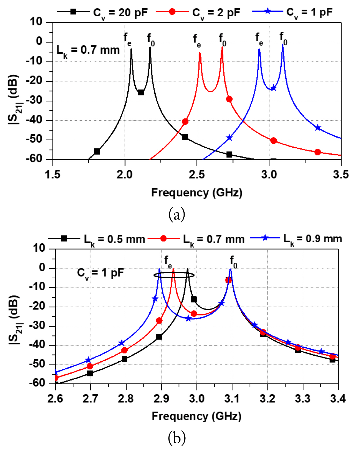
Fig. 4(a) shows the calculated resonant frequencies for different values of Cv. The frequencies fe and fo are tuned by changing the varactor diode capacitance from 1 pF to 20 pF. Similarly, Fig. 4(b) shows the simulated resonant frequencies for different values of Lk. Here, the value of Cv is maintained at 1 pF. As highlighted in this figure, the even-mode resonant frequency moves lower as the Lk increases, however, the odd-mode resonant frequency remains constant. These results confirm that the separation between the even- and odd-mode resonant frequencies can be controlled by Lk.

2. External Quality Factors

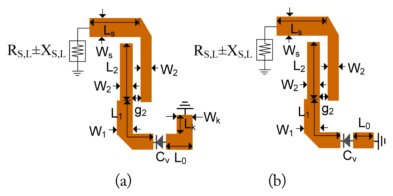
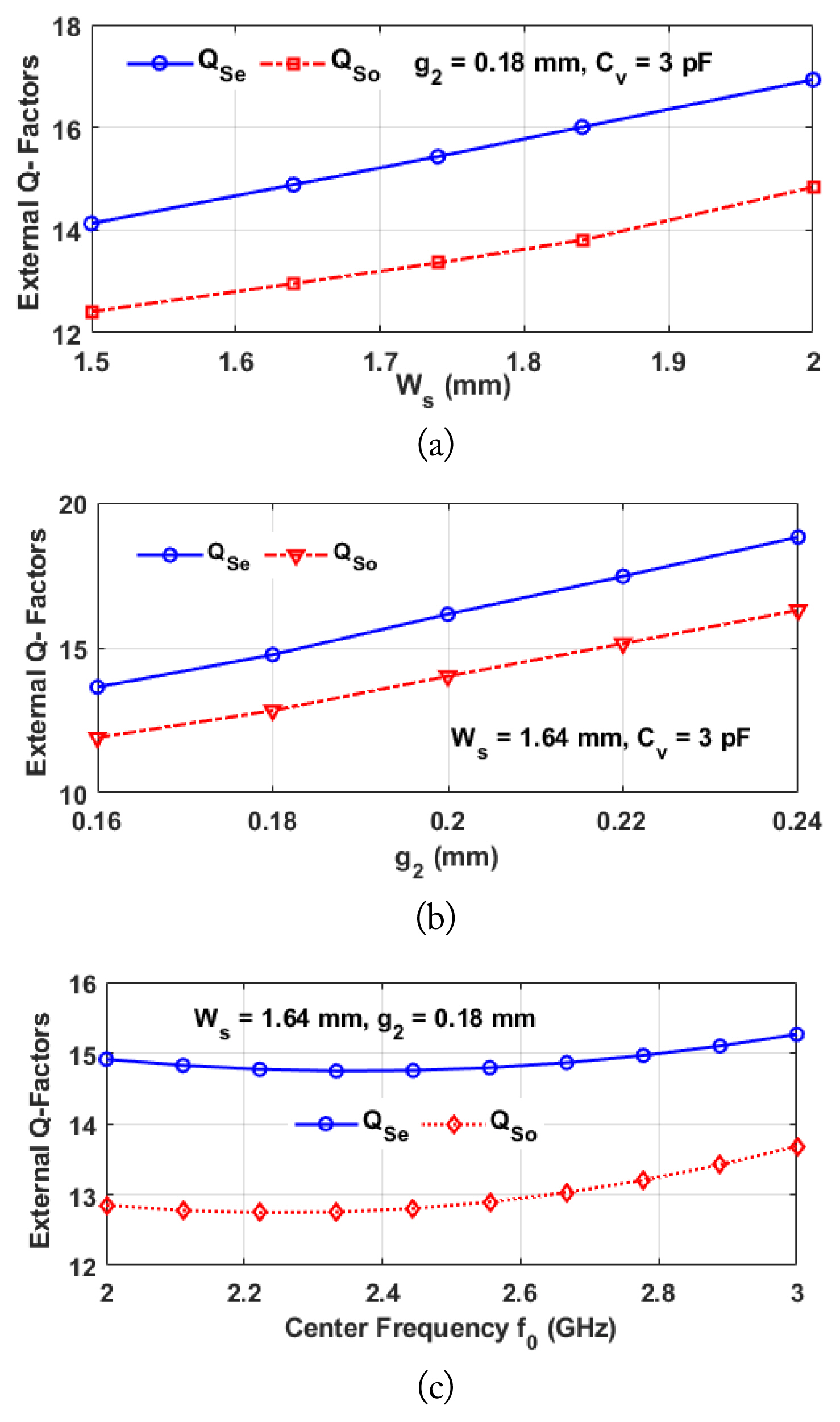
Fig. 5 shows the configuration of even- and odd-mode external Q-factors that are controlled by the series TL physical parameters Ws and Ls, as well as the coupled line physical parameter g2. The external Q-factors can be extracted using the method proposed in [20] as follows:
(10)
Qe=πfeτS11(fe)2,Qo=πfoτS11(fo)2,
where Qe and Qo indicate for even and odd-mode external Q-factors, respectively. Similarly, τs11 is the group delay at fe and fo.
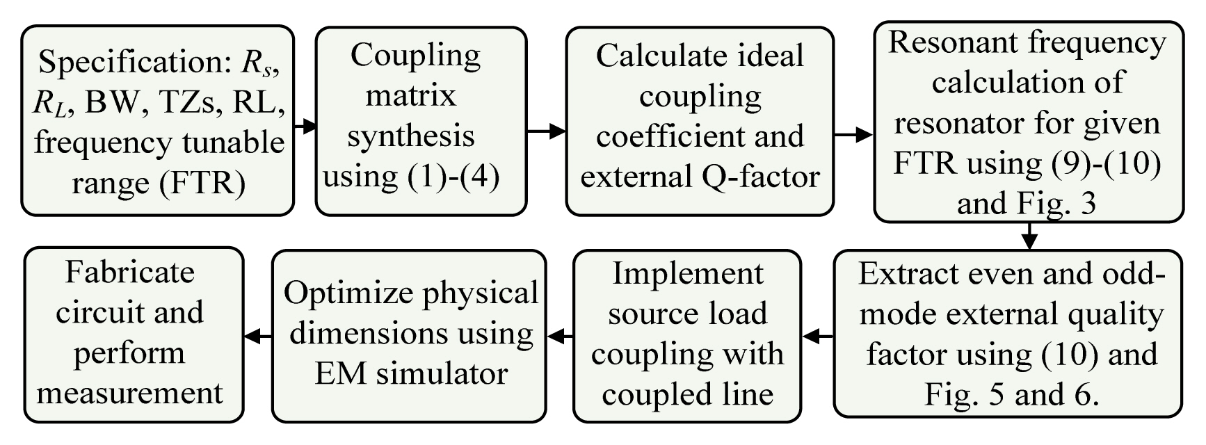
Fig. 6(a) and (b) show the extracted even- and odd-mode external Q-factors as functions of Ws and g2, respectively. The external Q-factors increases with the values of Ws and g2 and the desired external Q-factors are therefore obtained by controlling Ws and g2. Similarly, Fig. 6(c) shows the extracted Q-factor as a function of the center frequency. As indicated in this figure, the extracted Q-quality factors are nearly constant across a wide range of center frequencies. A summary of the step-by-step design method for the proposed BPF is provided in Fig. 7.
To validate the proposed arbitrary port-terminated tunable BPF, the simulation results of 50-to-50 Ω, 25-to-50 Ω and 20 + j10-to 50 Ω microstrip line BPFs as shown in Figs. 8 and 9, are compared with the coupling matrix synthesis results. The two TZs located at the lower and upper sides of the passband are generated by source-load coupling, which is implemented through a coupled line. The simulation results of microstrip line BPFs are consistent with the coupling matrix synthesis results.
These results indicate that the tunable BPF with input/output complex port impedances can be designed by modifying the input/output external quality factors and even-mode resonant frequency of the dual-mode resonator. The center frequency is tuned from 2.08 GHz to 3 GHz by varying the value of Cv from 1.16 pF to 60 pF. Moreover, the two TZs are also tuned as the center frequency is tuned.
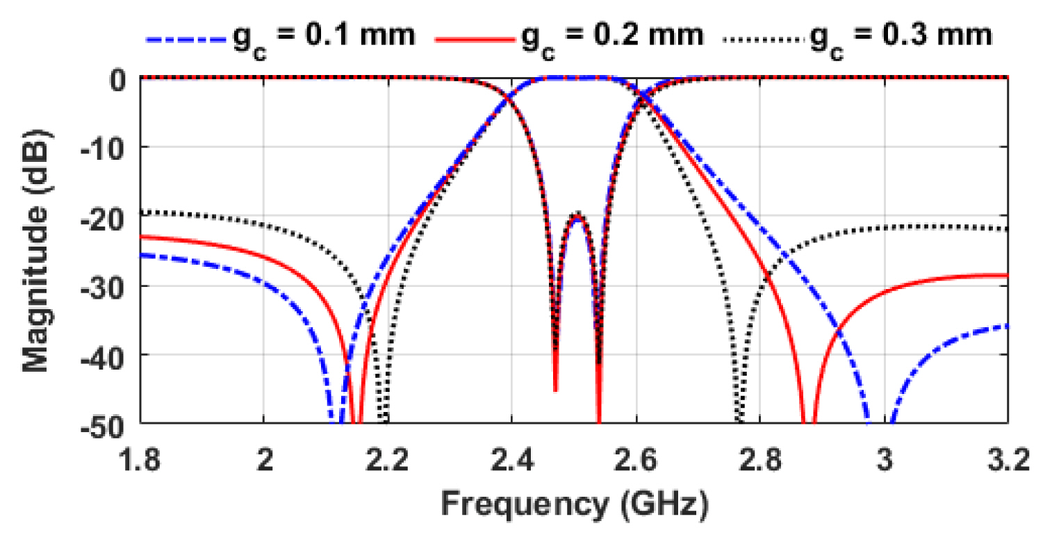
To investigate the effect of source-load coupling, the simulation results obtained with a different gap (gc) between the coupled lines, as shown in Fig. 10, are analyzed. As shown in the figure, the TZs move slightly away from the passband as the value of gc increases.

III. Simulation and Measurement Results

To experimentally validate the proposed BPF, three tunable BPF prototypes (50-to-50 Ω, 25-to-50 Ω and 20 + j10-to-50 Ω) are fabricated and measured using the Taconic substrate (dielectric constant ɛr = 2.20 and thickness h = 0.787 mm, and loss tangent tanδ = 0.0009). Each tunable BPF was designed using a Chebyshev response with a passband return loss of 20 dB for an FTR between 2.10 GHz and 3 GHz. Variable capacitances are implemented using varactor diode SMV 1233-079LF (Skyworks Corporation), which provides diode capacitance between 1.1 pF and 60 pF at 2 GHz by varying the reverse bias-voltage between 15 and 0 V. The physical dimensions of the fabricated the BPFs are shown in Table 1.
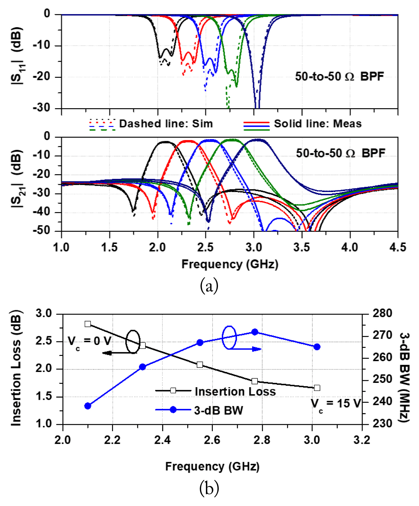
Fig. 11 shows the simulated and measured results of the 50-to-50 Ω (RS = RL = 50 Ω, Xs = XL = 0 Ω) tunable BPF. The measurement results are consistent with those of the simulation results, confirming that the center frequency is tuned from 2.1 GHz to 3.02 GHz (920 MHz or an FTR of 35.94%), while the insertion loss varies from 2.82 dB to 1.66 dB and the 3-dB BW varies from 238 to 265 MHz. Similarly, the measured return losses are better than 12.5 dB in the overall FTR.
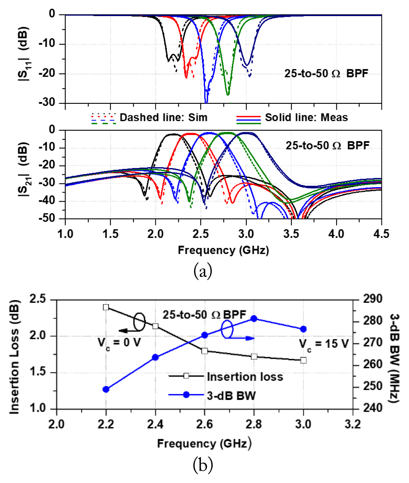
Fig. 12 shows the simulation and measurement results of the 25-to-50 Ω (RS = 25 Ω, RL = 50 Ω and Xs = XL = 0 Ω) tunable BPF. The measured center frequency is tuned from 2.2 GHz to 3.02 GHz (820 MHz) with an FTR of 31.42%. Similarly, the measured insertion loss varies from 2.4 dB to 1.67 dB whereas the 3-dB BW varies from 249 to 277 MHz. The measured return losses in the overall FTR are better than 12.5 dB.
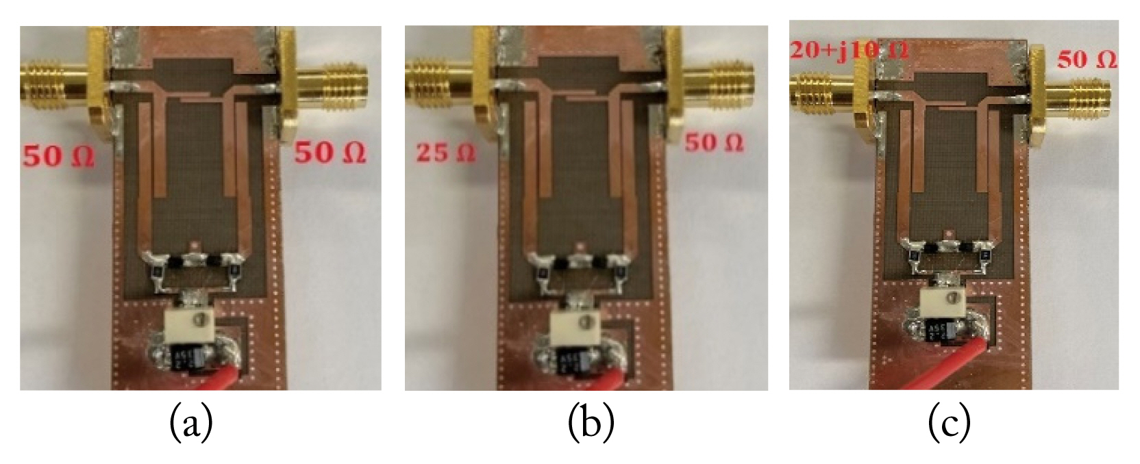
Fig. 13 shows the simulation and measurement results of the 20 + j10-to-50 Ω (RS = 20 Ω, Xs = 10 Ω and RL = 50 Ω, XL = 0 Ω) tunable BPF. The center frequency is tuned from 2.10 GHz to 3.01 GHz (910 MHz) with an FTR of 35.62%. Similarly, the measured insertion loss varies from 2.55 dB to 1.76 dB whereas 3-dB BW varies from 242 to 282 MHz. The measured return losses in the overall FTR are better than 12 dB. Photographs of the fabricated filters are shown in Fig. 14.
Table 2 compares the proposed tunable BPF with those described in previous studies. As observed from Table 2, the previously reported tunable BPFs have limited to a 50-to-50 Ω termination impedance filter design [1126]. Similarly, in [27] presents a direct coupling matrix synthesis of arbitrary input and output port impedances. In [28], a second-order all pole (without TZs) BPF with only one port complex impedance is demonstrated using substrate-integrated evanescent mode (EVA) cavity resonators. The work in [29] presents an active N + 3 coupling based BPF design by incorporating a transistor model for small-signal as input conjugately matched input impedance. In [30], the arbitrary input and output port complex impedances BPF without any TZs is designed and fabricated using an SIR. However, since these previous studies [2730] have experimentally demonstrated arbitrarily terminated BPF at a fixed center frequency, they might have faced difficulty in the physical realization of arbitrary input and output port impedance tunable BPFs. In contrast, the present study demonstrates arbitrarily terminated port impedance tunable BPFs (real-to-real and real-to-complex port impedances BPFs) over a wide FTR as well as two TZs. The result shows that the impedance transformer and frequency-selective tunable BPF can be integrated within a single circuit.

IV. Conclusion

In this paper, we demonstrated an arbitrarily terminated port impedances tunable BPF with transmission zeros. The proposed tunable BPF is based on a coupling matrix and a dual-mode tunable resonator. The designed tunable BPF with arbitrary termination impedance modified couplings between source/load and resonators of a 50-to-50 Ω BPF design. To validate the proposed design, three microstrip line tunable BPFs prototypes (50-to-50 Ω, 25-to-50 Ω, and 20+j10-to-50 Ω BPF) are designed and fabricated. The measurement results revealed that the center frequency is tuned across a wide frequency range.

Acknowledgments

This research was supported by National Research Foundation of Korea (NRF) grant funded by the Korea government (MSIT) (Grant No. 2020R1A2C2012057) and in part by the Basic Science Research Program through the NRF of Korea, funded by the Ministry of Education (Grant No. 2019R1A6A1A09031717).

Fig. 1
Structure of the proposed tunable BPF with arbitrarily terminated port impedance: (a) proposed BPF and (b) coupling diagram.
jees-2022-6-r-134f1.jpg
Fig. 2
Synthesis results of a tunable BPF using a coupling matrix with Δ = 4.4% and fc = 2.50 GHz.
jees-2022-6-r-134f2.jpg
Fig. 3
(a) Proposed structure of the dual-mode resonator, (b) even-mode equivalent circuit, and (c) odd-mode equivalent circuit.
jees-2022-6-r-134f3.jpg
Fig. 4
Resonant frequencies of the dual-mode resonator with Y1 = Yk = 1/70, Y2 = 1/60, L0 = 4.1 mm, L1 = 8.3 mm, L2 = 12.3 mm and various (a) Cv and (b) Lk. Substrate: Taconic with a dielectric constant of 2.2 and thickness of 0.787 mm.
jees-2022-6-r-134f4.jpg
Fig. 5
External Q-factor implementations: (a) even-mode and (b) odd-mode.
jees-2022-6-r-134f5.jpg
Fig. 6
External Q-factors with Ls = 10 mm, L0 = 3.86 mm, L1 = 8.26 mm, L2 = 12.3 mm, W1 = 1.36 mm, W2 = 1.20 mm, Wk = 0.25 mm, and Lk = 2 mm: (a) Ws, (b) g2, and (b) f0. Substrate: Taconic with a dielectric constant of 2.2 and thickness of 0.787 mm.
jees-2022-6-r-134f6.jpg
Fig. 7
Design flow chart of the proposed tunable BPF with arbitrarily terminated port impedances.
jees-2022-6-r-134f7.jpg
Fig. 8
Simulation results of the tunable BPFs: (a) 50-to-50 Ω BPF and (b) 25-to-50 Ω BPF. Solid line indicates coupling matrix and dashed line indicates transmission line circuit simulation.
jees-2022-6-r-134f8.jpg
Fig. 9
Simulation results of tunable 20 + j10-to-50 Ω BPFs. Solid line indicates coupling matrix and dashed line indicates transmission line circuit simulation.
jees-2022-6-r-134f9.jpg
Fig. 10
Simulation results with different transmission zero (TZ) locations according to gc.
jees-2022-6-r-134f10.jpg
Fig. 11
Simulation and measurement results of the 50-to-50 Ω BPF: (a) S-parameters, and (b) measured insertion loss and 3-dB bandwidth.
jees-2022-6-r-134f11.jpg
Fig. 12
Simulation and measurement results of 25-to-50 Ω BPF: (a) S-parameters, and (b) measured insertion loss and 3-dB bandwidth.
jees-2022-6-r-134f12.jpg
Fig. 13
Simulation and measurement results of 20 + j10-to-50 Ω BPF: (a) S-parameters, and (b) measured insertion loss and 3-dB bandwidth.
jees-2022-6-r-134f13.jpg
Fig. 14
Photographs of the fabricated tunable BPFs: (a) 50-to-50 Ω and (b) 25-to-50 Ω BPF, and (c) 20 + j10-to-50 Ω BPF.
jees-2022-6-r-134f14.jpg
Table 1
Physical dimensions of fabricated BPFs
50-to-50 Ω BPF (RS = 50 Ω, RL = 50 Ω, XS = XL = 0 Ω)
Ws Ls W2 L2 g2 W1
1.50 5 1.32 12 0.13 1.50
L1 L0 Wk Lk W3 L3
9 1.5 1.36 1.58 1.32 12
g3 WL LL WsL gsL LsL
0.13 1.2 5 0.6 0.13 4.8

25-to-50 Ω BPF (RS = 25 Ω, RL = 50 Ω, XS = XL = 0 Ω)

Ws Ls W2 L2 g2 W1
1.80 10 1.34 12 0.27 1.50
L1 L0 Wk Lk W3 L3
9 1.5 1.36 1.62 1.32 12
g3 WL LL WsL gsL LsL
0.14 1.20 5 0.4 0.13 4.8

20 + j10-to-50 Ω BPF (RS = 20 Ω, RL = 50 Ω, XS = 10 Ω, XL = 0 Ω)

Ws Ls W2 L2 g2 W1
2.1 8 1.30 12 0.30 1.50
L1 L0 Wk Lk W3 L3
9 1.5 1.36 1.62 1.32 12
g3 WL LL WsL gsL LsL
0.14 1.20 5 0.4 0.13 4.8

The dimensions are in millimeters.

Table 2
Performances comparison between the proposed design and those proposed in previous studies
Study Frequency (GHz) RS/RL (Ω) IL (dB) 3-dB BW (MHz) RL (dB) TZs NVR NCV
Gao and Rebeiz [11] 0.97–1.53 50/50 4.2–2.0 48–92a >10 Yes 7 4
Chiou and Rebeiz [12] 1.5–2.20 50/50 5.1–3.2 50–170a >10 Yes 9 3
Chiou and Rebeiz [13] 1.75–2.25 50/50 7.2–3.2 70–100a >10 Yes 5 2
Jung and Min [14] 0.255–0.455 50/50 1.8–1.40 70–76 >10 No 10 4
Chi et al. [15] 1.7–2.70 50/50 4.9–3.8 50–110 >10 Yes 7 4
Lu et al. [16] 0.70–1.78 50/50 4.5–2.0 70–98a >10 Yes 2 1
Chaudhary et al. [17] 2.36–2.85 50/50 3.52–1.45 NA >12 Yesb 3 2
Tang and Hong [18] 0.60–1.03 50/50 2.2–1.40 80–90 >10 Yesb 4 2
Lu et al. [20] 1.15–2 50/50 3.6–2.40 110–118a >10 Yes 2 1
Guo et al. [21] 1.35–1.60 50/50 4.90–2.30 NA >10 Yes 10 5
Chen et al. [22] 0.77–1.42 50/50 3.10–1.0 184–360 >10 No 6 3
Athukorala and Budi mir [23] 1.45–1.96 50/50 1.6–2.50 210–220 >10 Yes 2 2
Lu et al. [24] 0.8–1.21 50/50 3.8–1.8 130–140 >10 Yes 10 4
Lim et al. [26] 1.52–2.91 50/50 3.2–1.70 412–878 >10 No 3 1
Chen et al. [28] 3 3 – 5j/50 NA NA >12 No NA NA
Gao et al. [29] 10 NA NA NA >13 No NA NA
Kim and Jeong [30] 2.60 30 + 10j/50 0.89 140 >19.33 No NA NA
This work 2.10–3.02 50/50 2.82–1.66 238–265 >12.5 Yes 2 1
2.20–3.02 25/50 2.40–1.67 249–277 >12.8 Yes 2 1
2.10–3.04 20 + j10/50 2.55–1.80 242–285 >12 Yes 2 1

IL = insertion loss, RL = return loss, NVR = number of varactor diode, NCV = number of control voltage.

a 1-dB BW, TZs on both sides of passband frequency.

b TZs at only one side of passband frequency.

References

1. J.S. Hong and H.J. Lancaster, Microwave Filters for RF/Microwave Applications. Hoboken, NJ: John Wiley & Sons, 2004.

2. M. Rais-Zadeh, J.T. Fox, D.D. Wentzloff, and Y.B. Gianchandani, "Reconfigurable radios: a possible solution to reduce entry costs in wireless phones," Proceedings of the IEEE, vol. 103, no. 3, pp. 438–451, 2015.
crossref
3. A.J. Alazemi and G.M. Rebeiz, "A low-loss 1.4–2.1 GHz compact tunable three-pole filter with improved stopband rejection using RF-MEMS capacitors," In: Proceedings of 2016 IEEE MTT-S International Microwave Symposium (IMS); San Francisco, CA. 2016, pp 1–4.
crossref
4. S. Fouladi, F. Huang, W.D. Yan, and R.R. Mansour, "High-Q narrowband tunable combline bandpass filters using MEMS capacitor banks and piezomotors," IEEE Transactions on Microwave Theory and Techniques, vol. 61, no. 1, pp. 393–402, 2013.
crossref
5. B.W. Kim and S.W. Yun, "Varactor-tuned combline bandpass filter using step-impedance microstrip lines," IEEE Transactions on Microwave Theory and Techniques, vol. 52, no. 4, pp. 1279–1283, 2004.
crossref
6. K. Song, W. Chen, S.R. Patience, Y. Chen, A.M. Iman, and Y. Fan, "Compact wide-frequency tunable filter with switchable bandpass and bandstop frequency response," IEEE Access, vol. 7, pp. 47503–47508, 2019.
crossref
7. G. Chaudhary, H. Choi, Y. Jeong, J. Lim, D. Kim, and J. Kim, "Design of dual-band bandpass filter using DGS with controllable second passband," IEEE Microwave and Wireless Components Letters, vol. 21, no. 11, pp. 589–591, 2011.
crossref
8. G. Chaudhary, Y. Jeong, and J. Lim, "Harmonic suppressed dual-band bandpass filters with tunable passbands," IEEE Transactions on Microwave Theory and Techniques, vol. 60, no. 7, pp. 2115–2123, 2012.
crossref
9. B. Pal, M.K. Mandal, and S. Dwari, "Varactor tuned dual-bandpass filter with independently tunable band positions," IEEE Microwave and Wireless Components Letters, vol. 29, no. 4, pp. 255–257, 2019.

10. C. Chen, G. Wang, and J. Li, "Microstrip switchable and fully tunable bandpass filter with continuous frequency tuning range," IEEE Microwave and Wireless Components Letters, vol. 28, no. 6, pp. 500–502, 2018.
crossref
11. L. Gao and G.M. Rebeiz, "A 0.97–1.53 GHz tunable four-pole bandpass filter with four transmission zeros," IEEE Microwave and Wireless Components Letters, vol. 29, no. 3, pp. 195–197, 2019.

12. Y. Chiou and G.M. Rebeiz, "A tunable three-pole 1.5–2.2-GHz bandpass filter with bandwidth and transmission zero control," IEEE Transactions on Microwave Theory and Techniques, vol. 59, no. 11, pp. 2872–2878, 2011.
crossref
13. Y.C. Chiou and G.M. Rebeiz, "A quasi elliptic function 1.75–2.25 GHz 3-pole bandpass filter with bandwidth control," IEEE Transactions on Microwave Theory and Techniques, vol. 60, no. 2, pp. 244–249, 2012.
crossref
14. M. Jung and B.W. Min, "A widely tunable compact bandpass filter based on a switched varactor-tuned resonator," IEEE Access, vol. 7, pp. 95178–95185, 2019.
crossref
15. P. Chi, T. Yang, and T. Tsai, "A fully tunable two-pole bandpass filter," IEEE Microwave and Wireless Components Letters, vol. 25, no. 5, pp. 292–294, 2015.
crossref
16. D. Lu, X. Tang, N.S. Barker, and Y. Feng, "Single-band and switchable dual-/single-band tunable BPFs with predefined tuning range, bandwidth, and selectivity," IEEE Transactions on Microwave Theory and Techniques, vol. 66, no. 3, pp. 1215–1225, 2018.
crossref
17. G. Chaudhary, P. Kim, Y. Jeong, and J. Lim, "Dual-mode bandpass filter with independently tunable center frequency and bandwidth," In: Proceedings of the 2012 IEEE International Symposium on Radio-Frequency Integration Technology; Singapore. 2012, pp 56–58.
crossref
18. W. Tang and J.S. Hong, "Varactor-tuned dual-mode bandpass filters," IEEE Transactions on Microwave Theory and Techniques, vol. 58, no. 8, pp. 2213–2219, 2010.
crossref
19. G. Chaudhary and Y. Jeong, "Harmonic suppressed dual-band bandpass filter with independently tunable center frequency and bandwidths," Journal of Electromagnetic Engineering and Science, vol. 13, no. 2, pp. 93–103, 2013.
crossref
20. D. Lu, N.S. Barker, and X. Tang, "A simple frequency-agile bandpass filter with predefined bandwidth and stopband using synchronously tuned dual-mode resonator," IEEE Microwave and Wireless Components Letters, vol. 27, no. 11, pp. 983–985, 2017.
crossref
21. H. Guo, J. Ni, and J.S. Hong, "Varactor-tuned dual-mode bandpass filter with nonuniform Q distribution," IEEE Microwave and Wireless Components Letters, vol. 28, no. 11, pp. 1002–1004, 2018.

22. J.X. Chen, Y.L. Ma, J. Cai, L.H. Zhou, Z.H. Bao, and W.Q. Che, "Novel frequency-agile bandpass filter with wide tuning range and spurious suppression," IEEE Transactions on Industrial Electronics, vol. 62, no. 10, pp. 6428–6435, 2015.
crossref
23. L. Athukorala and D. Budimir, "Compact second-order highly linear varactor-tuned dual-mode filters with constant bandwidth," IEEE Transactions on Microwave Theory and Techniques, vol. 59, no. 9, pp. 2314–2320, 2011.
crossref
24. D. Lu, X. Tang, N.S. Barker, M. Li, and T. Yan Tang, "Synthesis-applied highly selective tunable dual-mode BPF with element-variable coupling matrix," IEEE Transactions on Microwave Theory and Techniques, vol. 66, no. 4, pp. 1804–1816, 2018.
crossref
25. J.R. Mao, W.W. Choi, K.W. Tam, W.Q. Che, and Q. Xue, "Tunable bandpass filter design based on external quality factor tuning and multiple mode resonators for wideband applications," IEEE Transactions on Microwave Theory and Techniques, vol. 61, no. 7, pp. 2574–2584, 2013.
crossref
26. T. Lim, A. Anand, J. Chen, X. Liu, and Y. Lee, "Design method for tunable planar bandpass filters with single-bias control and wide tunable frequency range," IEEE Transactions on Circuits and Systems II: Express Briefs, vol. 68, no. 1, pp. 221–225, 2021.
crossref
27. K.L. Wu and W. Meng, "A direct synthesis approach for microwave filters with a complex load and its application to direct diplexer design," IEEE Transactions on Microwave Theory and Techniques, vol. 55, no. 5, pp. 1010–1017, 2007.
crossref
28. K. Chen, J. Lee, W.J. Chappell, and D. Peroulis, "Co-design of highly efficient power amplifier and high-Q output bandpass filter," IEEE Transactions on Microwave Theory and Techniques, vol. 61, no. 11, pp. 3940–3950, 2013.
crossref
29. Y. Gao, X. Shang, and M.J. Lancaster, "Coupling matrix-based design of waveguide filters amplifiers," IEEE Transactions on Microwave Theory and Techniques, vol. 66, no. 12, pp. 5300–5309, 2018.

30. P. Kim and Y. Jeong, "A new synthesis and design approach of a complex termination impedance bandpass filter," IEEE Transactions on Microwave Theory and Techniques, vol. 67, no. 6, pp. 2346–2354, 2019.
crossref

Biography

jees-2022-6-r-134i1.jpg
Girdhari Chaudhary received his B.E. and M.Tech. degrees in Electronics and Communication Engineering from Nepal Engineering College (NEC), Kathmandu, Nepal and MNIT, Jaipur, India in 2004 and 2007, respectively, as well as a PhD degree in Electronics Engineering from Jeonbuk National University, Republic of Korea in 2013. He is currently working as a Contract Professor at JIANT-IT Human Resource Development Center, Division of Electronics Engineering, Jeonbuk National University, Korea. Previously, he worked as the Principal Investigator on an independent project through the Basic Science Research Program administrated by the National Research Foundation (NRF) and funded by the Ministry of Education. He is a recipient of the BK21 PLUS Research Excellence Award 2015 by the Korean the Ministry of Education. He is also a recipient of the Korean Research Fellowship (KRF) through the NRF funded by the Ministry of Science and ICT. His research interests include multi-band tunable passive circuits, in-band full duplex systems and high-efficiency power amplifiers and applications of negative group delay circuits.

Biography

jees-2022-6-r-134i2.jpg
Yongchae Jeong received his BSEE and MSEE, and Ph.D. degrees in Electronic Engineering from Sogang University, Seoul, Republic of Korea in 1989, 1991, and 1996, respectively. Between 1991 and 1998, he worked as a senior engineer at Samsung Electronics in Seoul, Republic of Korea. In 1998, he joined the Division of Electronic Engineering, Jeonbuk National University, Jeonju, Republic of Korea. Between July 2006 and December 2007, he worked as a Visiting Professor at Georgia Institute of Technology. At Jeonbuk National University, he had also served as Director of the HOPE-IT Human Resource Development Center of BK21 PLUS. Currently, he is a professor and Vice-President of Planning at Jeonbuk National University. His research interests include passive and active microwave circuit design, mobile and satellite base-station RF systems, periodic defected transmission lines, negative group delay circuits and their applications, in-band full duplex radio, and RFIC design. Prof. Jeong is a senior member of IEEE and a member of Korea Institute of Electromagnetic Engineering and Science (KIEES). He has authored and co-authored over 260 papers in international journals and conference proceedings.

ABOUT
ARTICLE CATEGORY

Browse all articles >

BROWSE ARTICLES
AUTHOR INFORMATION
Editorial Office
#706 Totoo Valley, 217 Saechang-ro, Yongsan-gu, Seoul 04376, Korea
Tel: +82-2-337-9666    Fax: +82-2-6390-7550    E-mail: admin-jees@kiees.or.kr                

Copyright © 2024 by The Korean Institute of Electromagnetic Engineering and Science.

Developed in M2PI

Close layer
prev next