Design of Compact Parallel-Connected Chained Function Filters
Article information
Abstract
The design of compact parallel-connected chained function filters is presented in this paper. The proposed filters will offer reduced sensitivity to manufacturing tolerance within the specified bandwidth in comparison to conventional Chebyshev filters for C-band applications. A new filtering function according to a chained configuration is derived for fourth-order filters, and the synthesis procedures are presented. To demonstrate the feasibility of this approach, the circuit simulation based on parallel-connected topology is performed in an advanced design system, while the design and simulation of a fourth-order filter in dielectric technology are carried out in high-frequency simulation software. The prototype of fourth-order microstrip topology is fabricated using open-loop resonators. The overall circuit size of the filter is 2.5 cm × 4 cm. The achieved simulation and measured insertion/return loss are 0.409 dB/20 dB and 2.674 dB/18.074 dB, respectively. Extensive sensitivity analysis is conducted to prove the fabrication tolerance of the filter. The reduced sensitivity of the proposed filter to manufacturing tolerance is fully demonstrated using an open-loop microstrip technology, and its reliability is proven by theoretical analysis. The prototype results in this research are validated and agree with the theoretical results. In terms of implementation, this design technique will be a very useful mathematical tool for any filter design engineer.
I. Introduction
Manufacturers are constantly under demand to minimize the time and cost of developing front-end millimeter-wave and microwave hardware for terrestrial and space applications [1]. High-performance filters are among the costliest components for such hardware, as they require high-quality materials, precise assembly, and, more importantly, post-manufacturing tuning [2]. Significant efforts have resulted in enhanced electromagnetic simulation tools in the context of such filters [3]. However, the improved simulation precision has shifted the focus of the problems to the manufacturing process [4]. To fully appreciate the benefits of enhanced modeling precision, the hardware must now be designed and produced with extremely low tolerance levels. Thus, the cost can rise [5]. Most millimeter-wave and microwave filters currently being developed and produced are made up of the conventional Chebyshev family [6]. This filter class has a specific filter order and offers the best rejection for an equiripple response [7]. The frequency distribution of return loss (RL) zeros in traditional Chebyshev filters is a crucial element for obtaining a good filter response [1, 8]. The relative frequency separation of RL zeros for narrow-band high-order filters becomes extremely small, necessitating a high accuracy in the manufacturing process [6]. Post-manufacturing tuning technique is applied to transform the filter response to the desired response [9]. To solve this issue, the filter’s sensitivity to the fabrication process and the constraints of existing production technologies must be addressed at the preliminary stage of approximation [10]. The desired filter specifications are simulated using a transfer function with higher order and reduced sensitivity. A new class of filtering function called chained is formed by combining the low-order functions of conventional Chebyshev polynomials [11]. The chained function polynomials can be found as a tradeoff between Butterworth and approximations of Chebyshev [12]. The technique offers several transfer functions to select from, each with unique properties and implementation requirements. Chained transfer functions can reduce filter complexity, manufacturing tolerance, and post-manufacturing tuning processes [3, 12]. Thus, they have the potential to extend current state of the art in higher-performance less-tuning filter production to higher operating frequencies and narrow bandwidth implementations.
This paper presents a new technique to design and implement the chained filtering function using a parallel-connected filter network. A fourth-order microstrip filter prototype is fabricated, and the measured results are included to prove the feasibility of this technique. The paper is sequenced as follows. Sections II and III present a clear theoretical analysis and chained function polynomial characteristics, respectively. Sections IV and V discuss the filter synthesis procedures and results, respectively. Section V presents the filter design and simulation using dielectric resonator technologies. Section VI presents the microstrip filter simulation results. Sections VII and VIII respectively discuss the filter prototype measured results and sensitivity analysis results. Finally, Section IX concludes.
II. Chained Function Characteristics
Fig. 1 demonstrates the characteristics of the chained function polynomial. The figure illustrates that the chained function passband ripple is a tradeoff between Butterworth and Chebyshev polynomial ripples. The ripples tend to overlap one another to form two poles spaced apart [12]. The closely spaced four-pole equiripple response is the Chebyshev model, which requires higher fabrication tolerance, while the Butterworth response has only one pole in the passband. The chained filtering function response can be achieved by selecting the appropriate seed-function order of {2,2} combinations. The selectivity of this filter will result in reduced sensitivity to fabrication tolerance compared to its Chebyshev counterpart, and its rejection performance is better than that of Butterworth but slightly less than that of conventional Chebyshev filters [13]. This filter class is not limited to sensitivity reduction but will lead to reduced complexity of filter design.
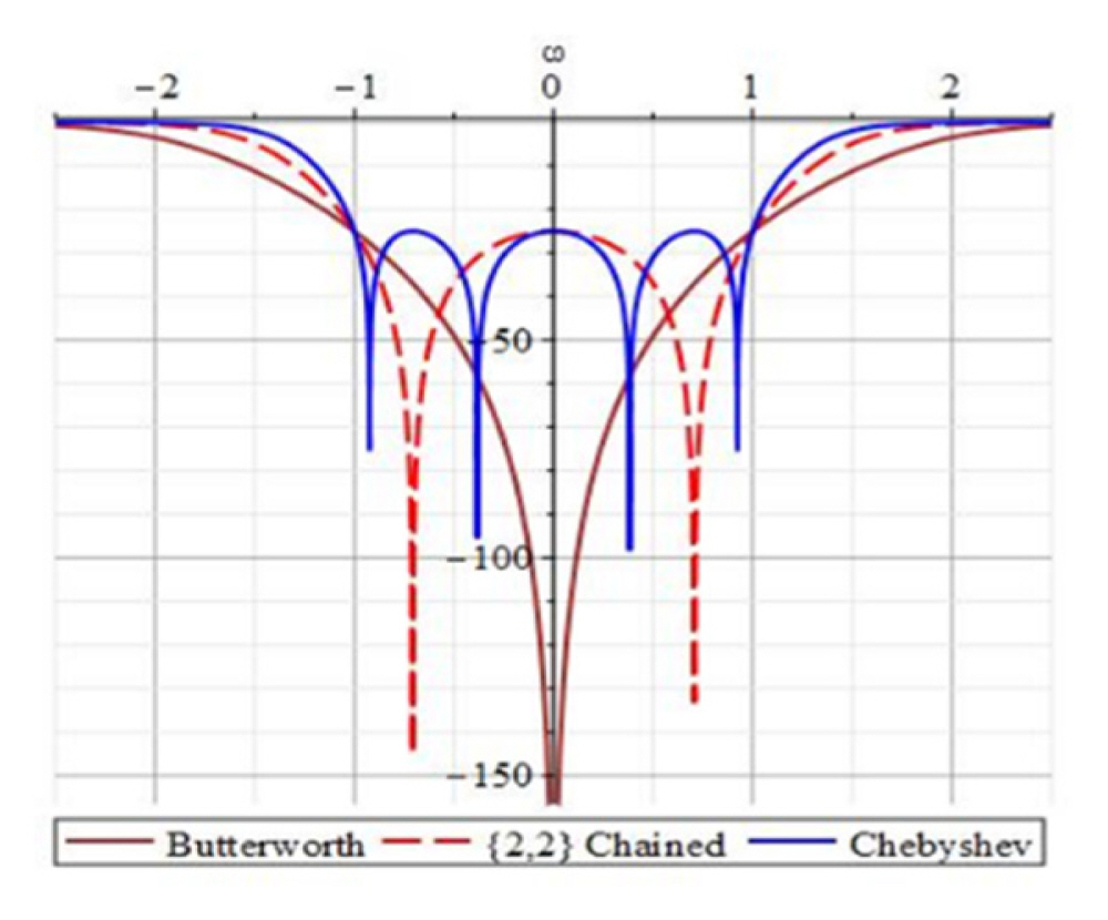
Chained function characteristics in comparison to the response of Butterworth and Chebyshev filters.
III. Chained Function Polynomial
A new polynomial generating function according to chained configuration can be defined using Eq. (1). This function is formed by multiplying the conventional Chebyshev product of lower-order functions called seed function. Each seed function has a selectable variety and provides ranges of transfer functions of the same degree, bandwidth, and RL level with different frequencies and implementation properties [11].
Eq. (1) is produced by multiple numbers of seed functions, each with a unique feature that allows it to fit within the predefined manufacturing constraints, thereby reducing the filter fabrication tolerance and production cost. Gμ(ω) is formed by the combination of the μ-seed function of Sns(k) and can be written as
where ns(k) is kth order seed function with a ms(k). nT represents the degree sum of constituent functions as defined in Eq. (3).
Table 1 illustrates chained combinations formed from the conventional Chebyshev lower-order seed-function polynomials for the fourth-order filter. The first row in Table 1 represents the Butterworth polynomial approximations, while the last row represents the conventional Chebyshev polynomial of the same order [14, 15].
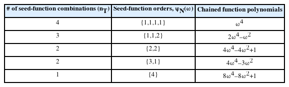
Chained function polynomial combinations for nT
IV. Parallel Chained Filter Synthesis Procedures
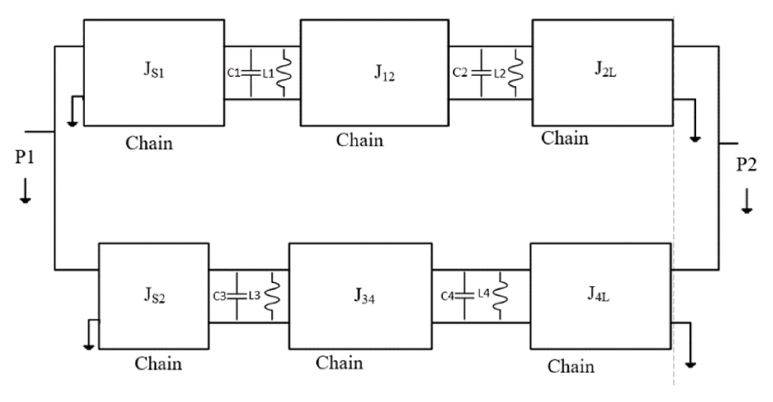
Consider the parallel chained connected coupled low-pass inverter network in Fig. 2.
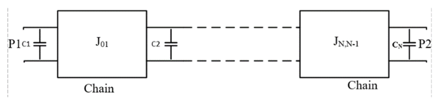
Parallel chained coupled low-pass inverter network.
The inverter network can be synthesized by solving the filtering function FN and S11, S21, defined as [2, 4]:
where ω is a frequency variable, FN is the filtering function, and ɛ is the ripple constant of 0.100503781.
The resonators are set up in parallel configurations by splitting using the partial fraction expansion in [2]. The even-mode admittance polynomial Ye can be derived by solving S11(p) roots as in [9, 10]. This function Ye is used to synthesize multiple branch resonators distributed across parallel-connected networks [4]. If the chosen circuit is symmetrical, then it is possible to solve any degree-ladder network, and for lossless networks, the even/odd mode reflection coefficients Se, So are expressed as [7, 8].
Ye and Yo can be further written as [5, 6]:
Eqs. (7) and (8) can be split by using partial fraction expansion to place the resonators in parallel configurations [1–4]. The parallel-connected chained transfer function can be written in terms of admittances based on the odd/even-mode reflection coefficients Se and So as expressed in [3, 13] to yield the following:
The matrix ABCD of the filter transfer function can be formed by choosing the appropriate expressions in [16, 17] and splitting them into partial fraction expansion, resulting in the placement of the resonators into a parallel network, [12, 18].
1. Fourth-order Parallel Chained Filter Synthesis
Fourth-order chained filtering function is formed by multiplying the {2,2} Chebyshev seed-function polynomial of the first kind. The synthesis technique is carried out first by deriving the even mode admittance [11, 19].
Step 1: The S-parameters are used to derive the zeros as follows:
Step 2: The left-hand plane polynomials are chosen as
Step 3: Ye, the chained filtering transfer function, can be derived as a two-branch parallel network, and then the roots of S11 and S21 are used to form the polynomial, P(p) as [3–5]:
Step 4: The zeros of P(p) are the same as the zeros of 1 + Ye(p) [2] and can therefore be derived using the formulas in [1, 6].
Step 5: The complex even/odd mode polynomials are obtained from Eqs. (15)–(18).
By using Eq. (15),
Step 6: From Eq. (18), an even-mode admittance inverter of 1 can be positioned before the network. Thus, Ye can be written as
Sep 7: The denominator is factorized using a partial fraction expression and
Step 8: The same technique can be extended to generate the same results in the odd-mode admittance network as follows:
The numerator values are the J-admittance, and the denominator is the capacitance values [1]. Ye, Yo can be further split down to a four-parallel network branch by dividing (24) by 2.
Hence,
The parallel network in Fig. 3 is formed using the admittance values derived for the even mode in Eq. (24). The circuit simulation S-parameter response is shown in Fig. 4.

Fourth-order two-branch parallel chained low-pass network (C1 = C2 = 1.0807 F, C3 = C4 = 2.1578 F, JS1 = J2L = 1, JS1 = J2L = 1, J12 = 0.8282, J34 = −3.3023).
Fourth-order low-pass filter S-parameter response.
The low-pass filter network can be transformed into a bandpass filter by applying the appropriate transformation expressions in [5, 15, 20]. The transformation network is shown in Fig. 5, and the S-parameter response is presented in Fig. 6.
Fourth-order two-branch parallel chained band-pass network (C1 = C2 = 991.423 pF, C3 = C4 = 748.35 pF, L1 = L2 = 0.0021 nH, L3 = L4 = 1.014).
Fourth-order parallel chained band-pass S-parameter response.
This design technique is useful for synthesizing circuits in different parallel configurations, such as four- and six-branch parallel networks [19].
2. Parallel Chained Filter Coupling Matrix Synthesis
The filter coupling matrix is mapped by chaining the seed functions generated from the polynomial function ψN(ω) [20]. The transmission and reflection coefficients S11 and S21, which are used to derive the coupling matrix for the filter network, are as follows:
where ω is the complex frequency parameter s = jω, and FN(ω), EN(ω) are the Nth-order filter polynomials of the chained functions [21]. The polynomials Es, Fs are applied to derive the even/odd-mode polynomials [22]. The parameters for short-circuit admittance y21, y22 can be derived from (29), and N which represents the even/odd mode.
where λk represent the pole for eigenvalue, and T1k and TNk are the respective orthogonal first and last rows of the matrix T. The orthogonal rows can be generated by using the Gram-Schmidt orthogonalization technique [21]. Similarity transformation and matrix element annihilation are performed and the complete coupling matrix M is obtained [22, 23]. To synthesize the coupling matrix of two pole parallel networks, the matrix is divided into subnetworks and a series of configurations are carried out for the entire matrix until the right coupling is achieved [14]. The full coupling matrix (M) for the fourth-order parallel chained filter is shown in Eq. (30), and the N+2 configuration routing structures are in Fig. 7.

Fourth-order filter coupling routing topology.
V. Simulation Results of Parallel Chained Dielectric Resonator Filter
1. Dielectric Resonator Configurations
Fig. 8 shows a single resonator mounted inside a squared cavity assumed to have a parameter defined as cavity width (Cx, Cy), cavity length (Cz), resonator diameter (Dr), resonator height (Lr), low permittivity dielectric support diameter (Ds), and support height (Ls). The chosen dielectric resonator is cylindrical and has a low dielectric permittivity. The design parameter values are defined in Table 2.

Dielectric resonator configuration inside an enclosure.

Dielectric resonator dimensions
2. Dielectric Resonator Mode Chart
The eigenmode solver window in High-Frequency Simulation Software (HFSS) is used to generate the mode chart as proof of the design idea. By increasing the resonator puck diameter to height ratio, the simulation is run multiple times. The diameter remains constant while the size of the resonator puck is reduced by half. It can be observed that as the ratio of D/L increases, the resonant frequencies of each mode will increase accordingly. This effect demonstrates that the resonant frequency can be designed to the desired frequency by adjusting the ratio of D/L [1]. Fig. 9 shows the resulting mode chart diagram for the first four modes of the dielectric resonator obtained using HFSS.
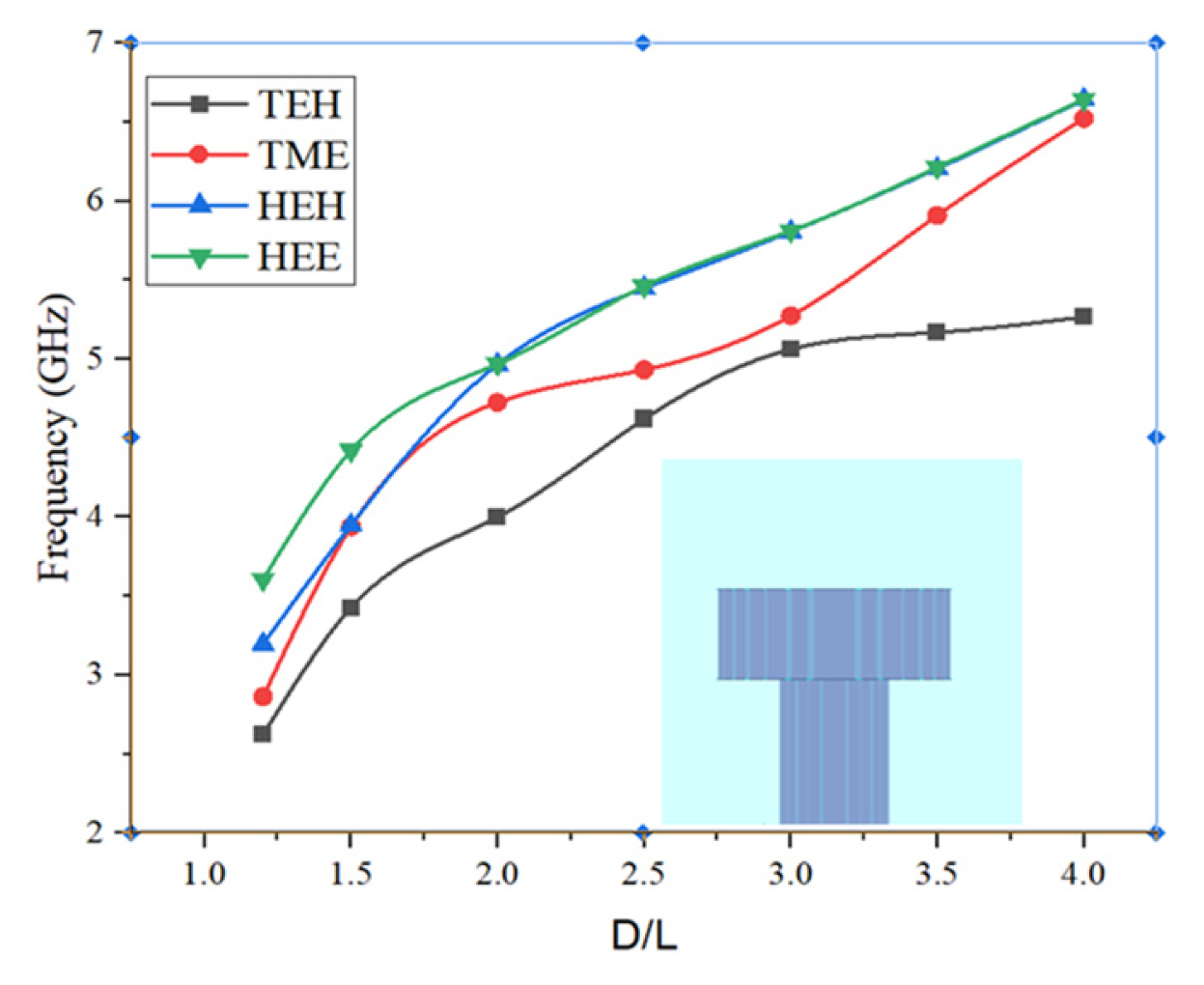
Mode chart of the first four dielectric resonator modes.
3. Dielectric Inter-Resonator Coupling
Achieving good coupling between resonators is based on extracting the external quality factor (Qe) and coupling coefficient (K) to form a parallel-connected network using Eqs. (31) and (32). We begin by investigating the coupling between two resonators that are symmetrically divided into separate resonators and terminated by either an electric wall or a magnetic wall. The coupling is determined by using the resonance frequency of the two distinct resonators [23, 24]. The coupling matrix (M) elements are normalized to the fractional bandwidth. Matrix M is a coupling element between two adjacent resonators. Fig. 10 shows the two coupled resonators together with their corresponding plot of coupling coefficient K versus W. The original cavity dimensions can be used to find the resonant frequencies for both even and odd modes in HFSS.
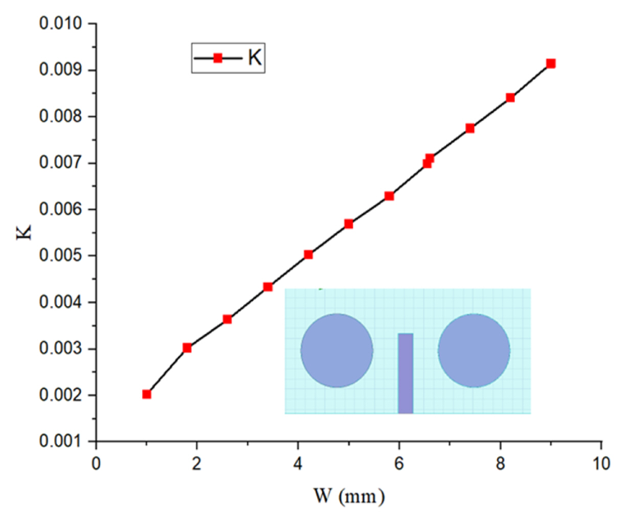
The coupling K plot against the width iris W.
The first eigenmode frequency is f1, the second is f2, the center frequency is fo, and R1 is the coupling resistance. The normalized coupling coefficient K and the filter bandwidth (BW) are all defined.
It can be observed in Fig. 9 that the coupling gap (W) increases as the coupling coefficient (K) increases, and vice versa. The weaker coupling results in a lower coupling coefficient and a strong coupling in a higher coupling coefficient.
4. Fourth-Order Dielectric Filter Simulation
The filter design and simulation are carried out using the ANSYS HFSS driven-model approach. The chained function polynomial ψN(ω) = 4ω4–4ω2+1 with the seed function of order {2,2} is transformed into a parallel network using dielectric resonators. The target center frequency of the filter is 3.5 GHz, with an RL of 20 dB and a fractional bandwidth of 0.67%. Fig. 11 shows the 3D-designed structural setup of the bandpass filter. The Iris thickness is maintained at 3 mm for all irises. The design is achieved by adjusting the dimension of one resonator branch with the connecting irises and the input probe until the desired response is attained. The process is repeated by inserting the output probe and the branch of the next resonator at the same time. The final parameters of the topology after the tuning process are D1 = D2 = D3 = D4 = 14.602 mm, W12 = W34 = 5.01 mm, and W14 = W23 = 5.1 mm. The S-parameter response of the filter is shown in Fig. 12. The center frequency is 3.5 GHz with a fractional bandwidth of 0.5%, and an RL level of 20 dB is achieved. The results are in good agreement with the theory.

Fourth-order parallel chained dielectric resonator 3D topology.
Simulation S-parameter response of the dielectric filter.
VI. Simulation Results of Parallel Chained Microstrip Filter
1. Microstrip Filter Inter-Resonator Coupling
The initial filter design parameters are the center frequency of 3.5 GHz, a bandwidth of 200 MHz, an insertion loss (IL) of <3 dB, and an RL of 20 dB. The microstrip substrate of Rogers RT/duroid 5880, with a thickness of 787 μm and a relative dielectric constant ɛr of 2.2 is used for the filter implementation [25–27]. The open-loop resonator is selected for this design because of its simplicity of manufacturing. The suitable electrical length at resonance is 180°. The coupling configuration between the adjacent resonators is a mixed coupling [24, 25]. The coupling coefficient (K) values in Table 3 are obtained using the line calculation approach in an Advanced Design System (ADS) simulation software.
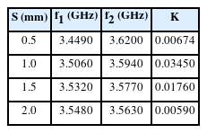
Coupling coefficient versus the resonator gap (S)
Fig. 13 illustrates the plot of the coupling coefficient and gap or distance between resonators. The gap or distance (S) increases as the coupling coefficient (K) decreases. Smaller coupling coefficients mean weaker resonator coupling.

Filter coupling coefficient (K) versus the resonator gap (S).
2. Fourth-Order Parallel Chained Microstrip Filter Design and Simulation
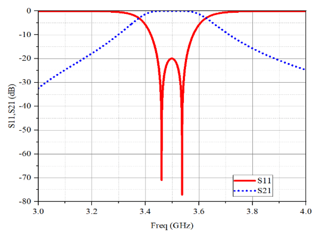
The polynomial function according to chained Gμ(ω) = 4ω4–4ω2+1 and seed order {2,2} is chosen. This function is transformed into a physical parallel network for optimum realization. The design is achieved via an ADS using open-loop microstrip resonators [28, 29]. The resonators are all connected in parallel and chained to the filter output. The simulated IL/RL achieved is 0.409 dB/20 dB. The out-of-band rejection observed is better than 18 dB. The final physical layout of the filter is shown in Fig. 14, and the corresponding S-parameters response is in Fig. 15.
Fourth-order parallel chained filter physical layout.
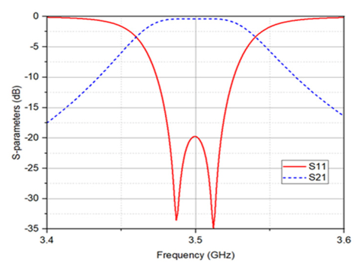
Filter simulation S-parameter response.
From the S-parameter responses achieved, the filter produced two poles as expected for chained function implementations. This outcome serves as the main benefit of chained function polynomials, which efficiently place multiple RL zeros at the same frequency, resulting in filters with reduced sensitivity to manufacturing error while preserving their response within the specified passband [27, 30]. In terms of theoretical analysis, the filters have proven to offer good rejection levels comparable to the Chebyshev filters, which are dependent on the proper seed-function selections.
VII. Prototype Design Results
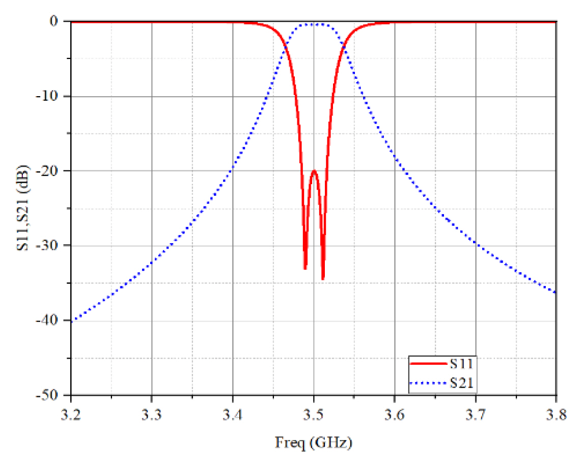
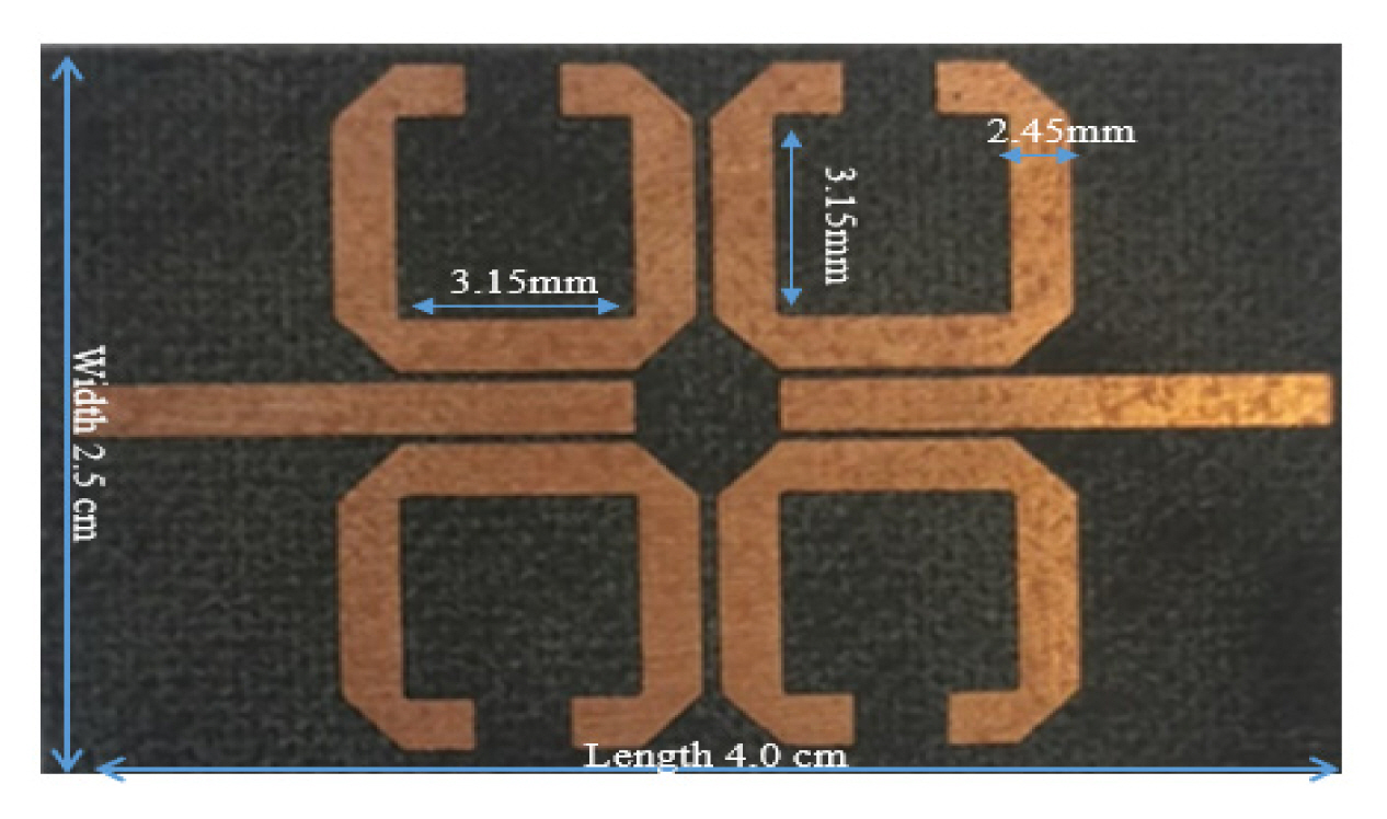
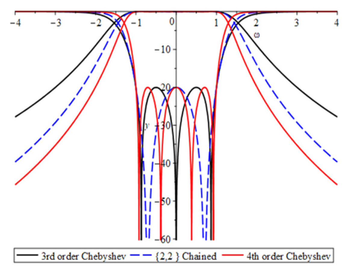
Rogers RT/duroid 5880 microstrip substrate with a thickness of 787 μm and 2.2 relative dielectric constants is used [31, 32]. The width and length of the resonator are 2.45 and 3.15 mm, respectively. The input/output ports are attached to an SMA 3.5 mm connector, and the feed lines between the resonators and connectors are 10 mm long. The filter prototype is shown in Fig. 16. The overall circuit size of the filter is 2.5 cm × 4 cm. The measured and simulation responses are shown in Fig. 17. The filter has proven the ability to produce two resonance poles within the desired bandwidth with a center frequency of 3.5 GHz achieved. The values of simulated and measured IL/RL achieved are 0.409 dB/20 dB and 2.674 dB/18.074 dB, respectively. There is a shift in the center frequency of the measured result compared to the simulation result. The shift is caused by discontinuities in the microstrip line junction, radiation, package parasitic, and dielectric loss of the material [26]. The transmission zeros of the filter can be controlled by changing the source capacitor values and the load coupling. This finding agrees with the theoretical analysis. Table 4 compares the results in this work with state-of-the-art implementations [17, 27, 30–33].

Microstrip prototype of parallel-connected chained function filter.

Simulated and measured transmission and reflection responses of parallel-connected chained filter.
Comparison with related work
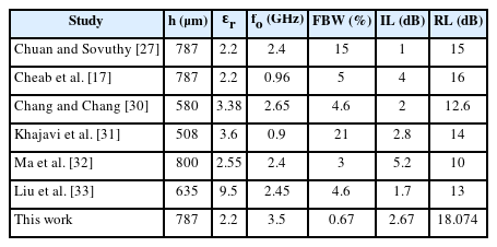
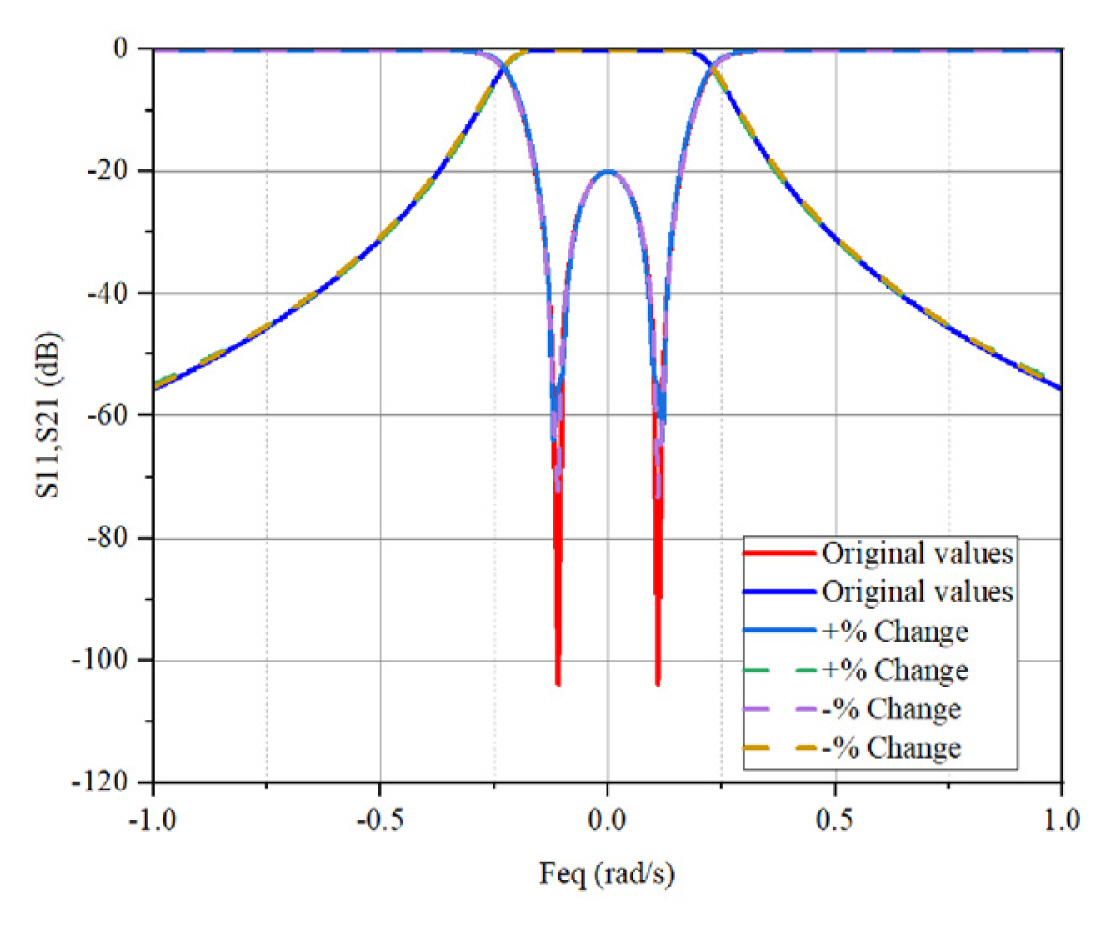
VIII. Sensitivity Analysis
Sensitivity analysis is conducted on parallel-connected chained-function filters to prove that the filters can be fabricated with better tolerance and their response preserved within a specified bandwidth in comparison to Chebyshev filters. To assess the effects of manufacturing tolerance, several experiments are conducted where the initial component values are changed to have differences of ± 1% and ± 2%. The distribution’s variance is chosen to provide a maximum error of approximately 5 μm, specified as the maximum tolerance of filter fabrication machines. The shifts in the passband for parallel chained function filters are recorded to be ± 0.025% and ± 0.07% compared to their original values and the Chebyshev counterparts, and the RL shifts are ± 1.5% and ± 2.5%. In all cases, the RL remains at 20 dB and is maintained. Figs. 18 and 19 show the result of this analysis. These findings greatly prove that parallel-connected chained function filters are less sensitive to manufacturing error and can preserve selectivity. This finding is demonstrated by the reduced percentage shift in RL distributions when random tolerance is applied. The further apart placement of the filter poles is evident, confirming higher manufacturing tolerance.
±0.025% and ±0.07% tolerance applied on fourth-order parallel chained function filter.
±0.025% and ±0.07% tolerance applied on the fourth-order Chebyshev filter.
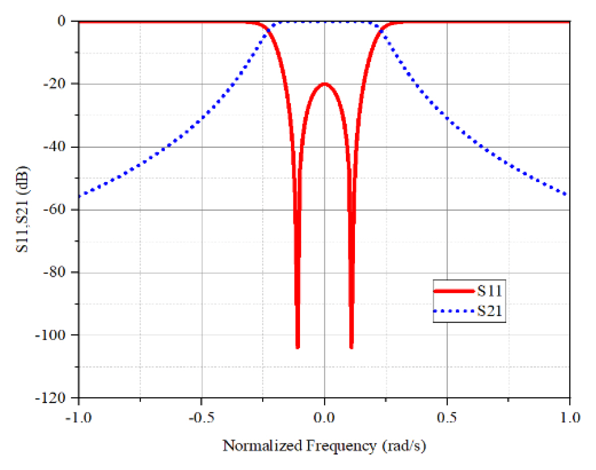
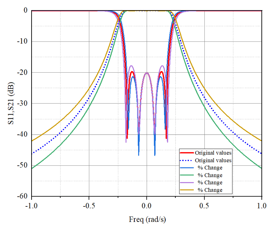
1. Comparison of Fourth-Order Parallel-Connected Chained Filter to Fourth- and Third-Order Chebyshev Response
Compared to Chebyshev’s third- and fourth-order filters, the chain function filter rejection is proven to be higher than that of the third-order Chebyshev but slightly lower than the fourth order. The passband of the chained function has only two poles placed further apart than those of the third-order Chebyshev response. The ability of the chained function polynomial to place multiple RL zeros at the same frequencies will result in the filter being less sensitive to fabrication error and still retaining the desired out-of-band rejection [5, 33]. Fig. 20 shows the theoretical comparison plot.
Comparison response of the chained function {2,2} order compared to Chebyshev’s third and fourth order.
IX. Conclusion
Fourth-order parallel-connected chained function filter prototypes are designed and fabricated. The overall circuit size of the filters is 2.5 cm × 4 cm. The filter achieves a measured IL/RL of 2.674 dB/18.074 dB. The theoretical and measured results are in good agreement with each other. Extensive sensitivity analysis is conducted, and the results prove the fabrication tolerance of the filter. The advantage of this filter prototype is that it offers reduced sensitivity to manufacturing tolerance while retaining rejection performance that is comparable to a conventional Chebyshev filter. The reduced sensitivity to manufacturing tolerance is fully demonstrated using an open-loop microstrip technology, and its reliability is proven. In terms of implementations, the filter is not limited to microstrip technology but can be applied to any given technology available. Lower- and higher-order filters can be easily implemented using chained function polynomials, thereby serving as a very useful mathematical tool for any filter design engineer.
Acknowledgments
The authors would like to thank YUTP (No. 015LC0-320) for providing the funding that allows this research to be viable and successful. The authors also appreciate all the individuals who have contributed directly or indirectly to complete this project.
References
Biography
Francis E. Chinda was born in 1983. He received his B.Eng. degree in Electrical and Electronics, major in Electrical and Electronics, from the prestigious University of Maiduguri, Nigeria. He completed his MSc in Electronic Communication and Computer Engineering from the University of Nottingham, United Kingdom, in 2015 and is currently pursuing a Ph.D. at Universiti Teknologi PETRONAS, Malaysia. He is also a Teaching/Research Assistant with the Department of Electrical and Electronic Engineering, Universiti Teknologi PETRONAS. His research interests include the design and synthesis of microwave bandpass filters for 5G, satellite, and millimeter-wave applications. Currently, he is working on passive filter design, implementation, and testing for RF front-end subsystem applications.

Socheatra Soeung was born in Phnom Penh, Cambodia, in 1986. He received his B.Eng. (Honors) degree in Electrical and Electronics, majoring in Computer System Architecture, in 2010 from Universiti Teknologi PETRONAS, Malaysia. He completed his MSc and Ph.D. degrees by research in RF Microwave Engineering at Universiti Teknologi PETRONAS, Malaysia in 2013 and 2018, respectively. He worked as a research officer under the project “Wireless Communication Using Evaporation Duct (WiDuct)” with the responsibility for RF front-end design, implementation, and testing. Currently, he works as a lecturer at Universiti Teknologi PETRONAS in the Electrical and Electronic Engineering Department. His research interests include passive filter design and synthesis, computer-aided tuning, and optimization techniques. He is currently an IEEE, MTT member, and committee member of IEEE ED/MTT/SSC Penang Chapter, Malaysia.
Sovuthy Cheab (M’15) holds a B.Eng. (Hons) in Electrical and Electronic Engineering, MSc, and Ph.D. in RF and Microwave Engineering from Universiti Teknologi Petronas. Before entering the industry, he worked as a lecturer for six years in the Electrical and Electronic Engineering Department, Universiti Teknologi PETRONAS, teaching electromagnetic theory, communication systems, and RF/microwave-related subjects. He supervised a total of 6 Ph.D. and 7 master’s students. In terms of research, he has secured many national and industry grant projects. Dr. Cheab has been an Executive Committee Member of the IEEE ED/MTT/SSC Penang Chapter since 2016 and was elected as the secretary of the Chapter for the 2021–2022 term. He served as the secretary of IMESS 2018, the MTT Technical Chair of IMESS 2019, and the Publication Chair of the ICIAS 2020 conference. He is a technical consultant on the design and synthesis of RF and microwave passive filters and other components for 5G applications and beyond. Currently, he is working on the design, simulation, and fabrication of the RF and microwave narrow band and broadband circulators. He now works for FILPAL (M) Sdn Bhd as the Technical Director. His role includes leading the training division in the company.
Muhammad S. Yahya (Student Member, IEEE) received his B.Eng. degree in Electrical and Electronics Engineering from Abubakar Tafawa Balewa University Bauchi-Nigeria (2010) and M.Eng. in Electronics and Telecommunications Engineering from Universiti Teknologi Malaysia (2016). He is currently pursuing his Ph.D. in Electrical and Electronics Engineering at Universiti Teknologi PETRONAS Malaysia. His research interests include antennas and propagation and RF/microwave circuits.
Huzein Fahmi Bin Hawari received his degree in Electrical and Electronics Engineering from the University Science of Malaysia (USM) in 1999 and a Master in Electronics Engineering from the University Technology of Malaysia in 2008. In 2015, he completed his Ph.D. at Universiti Malaysia Perlis (UniMAP), major in Mechatronics Engineering. In 1999, he joined Intel Microelectronics where he held various key posts, such as staff product engineer with Intel Design Centre. His last position with Intel was as a staff system validation, where he was responsible for the solid-state devices (SSD) system validation startup in Intel Malaysia. He is currently attached to the Department of Electrical and Electronics Engineering, Universiti Teknologi PETRONAS, Malaysia, as a senior lecturer, where he is also a Senior IEEE Member and registered Professional Engineer with the Board of Engineers, Malaysia. His research and interest fields are MEMs, sensors, nanodevices, sensor and communication systems, the Internet of Things (IoT), and deep learning.