I. Introduction
Modern wireless network standards have adopted higher modulation schemes in a bid to improve data rates while preserving the integrity of the highly packed data bits in each symbol transmission. The downside of these multi-carrier modulation schemes is the generation of signals with large peak-to-average power ratio (PAPR). Most importantly, the suitability of the power amplifier unit to efficiently amplify these signals while preserving a low error vector magnitude is critical to the successful operation of any transceiver unit.
Over the years, the Doherty power amplifier and the Chireix outphasing amplifier have been among the widely deployed amplifier architectures for designing highly efficient and linear radio frequency power amplifiers [1, 2]. Recently, however, the load modulated balance amplifier (LMBA) architecture has drawn significant interest [3].
In the conventional balanced amplifier, it was discovered that when a signal is fed at the isolation port of the output coupler, the balanced amplifier devices experience a load modulation effect [4]. Moreover, this modulation is isolated and independently controllable by what is termed as an amplitude and phase control. This characteristic has driven more research into the LMBA resulting in multiple variants, including the RF-input LMBA where a single supply is used for both the main balanced amplifier stage and the auxiliary control signal [5]. This resulted from the initial topology, which had independent supplies for both the balanced amplifiers and the auxiliary device. Thus, eliminating this dual input also got rid of the need for a regulated independent control signal.
In [6], the authors performed an in-depth analysis of the LMBA operation and illustrated a design technique for RF-input LMBA with Doherty-like efficiency enhancement characteristics. Another variant was also proposed in which the operations of the main balanced amplifier and the auxiliary amplifier are completely flipped [7]. Known as the “pseudo-Doherty LMBA,” the main balanced amplifier operates in the high-power region, whereas the auxiliary device sets off in the low-power region. Several other published works [8–11] that have adopted this approach have reported incredible performance, including an extended output power back-off range of up to 12 dB, with one even achieving a dual octave bandwidth operation [10]. Another variant, the orthogonal LMBA that eliminates the extra control signal device, has also been published [12]. Here, the control signal is fed at the isolation port of the balanced amplifier input coupler, and its main advantage is that the control signal gets amplified with the same efficiency as the principal signal without the need for an extra amplifier.
Broadening the LMBA horizon, this paper presents an LMBA with a two-stage control signal power amplifier. At the input, the power is split with an uneven Wilkinson divider, and through an empirical analysis, the optimal power splitting ratio for an optimal amplitude modulation is determined. A generalized load-pull analysis for the output matching network is used to determine the optimal impedances for the target efficiency peaks in the low- and high-power regions. At the same time, the second harmonic is well terminated alongside the output matching network. This in turn preserves the optimal load trajectory for high efficiency and a flat gain response, which allows for improved efficiency and linearity trade-off. To the authors’ knowledge, this topology has yet to be studied or published. A detailed analysis of the design and operation of this newly designed topology is presented and experimentally verified targeting the 3.3–3.8 GHz range.
II. Proposed LMBA Design
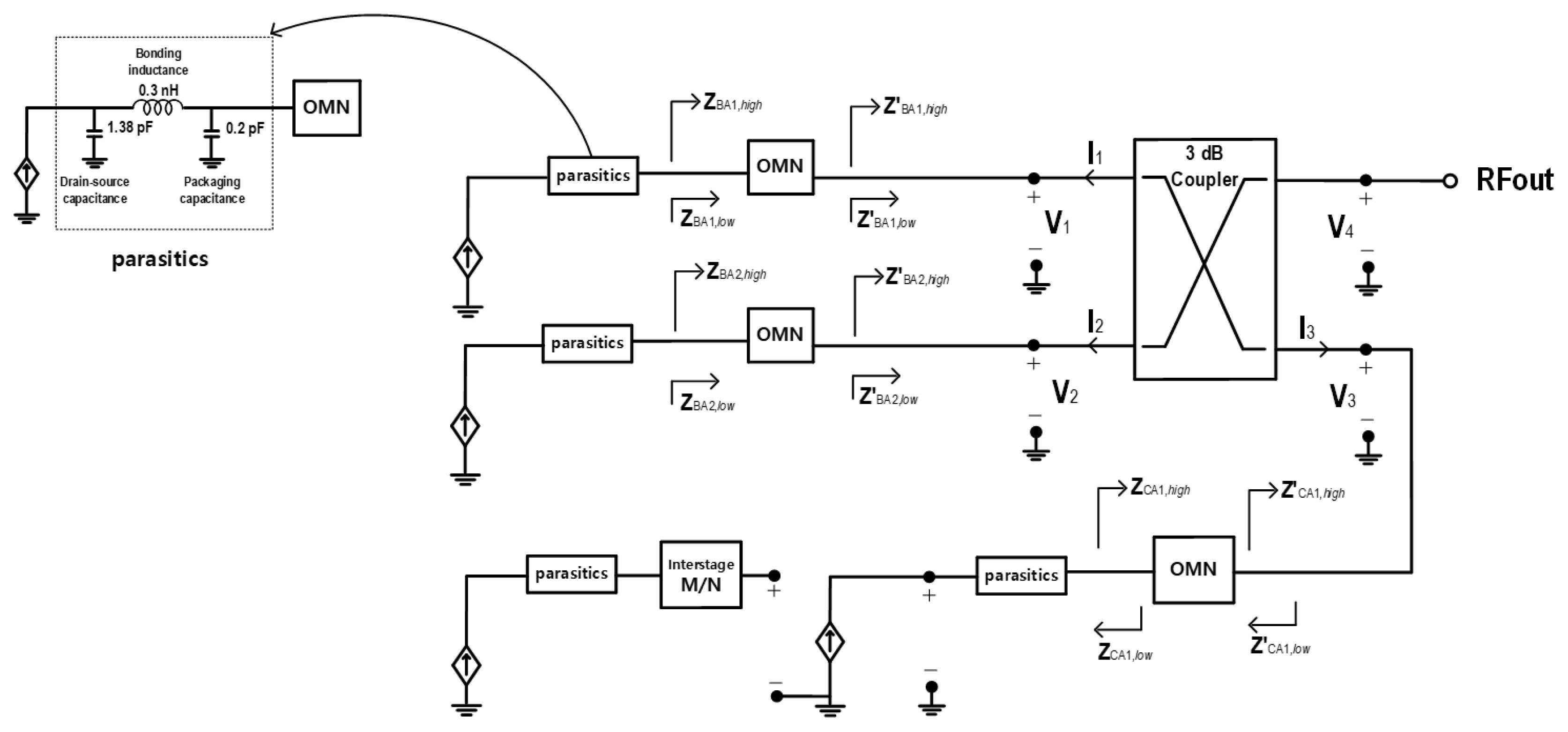
The LMBA was first introduced by applying the classical balanced amplifier to a control signal amplifier, which then modulates the balanced pair through the isolation port of the output 3 dB coupler. As the power through the port varies in amplitude and phase, the modulation effect is then realized. This phenomenon can be studied through the four-port Z-parameters of the 3 dB coupler and the current from each branch [13, 14]. As shown in Fig. 1, the equal amplitude quadrature current signals of the balanced pair can be represented as follows: bI1 and bI2, where b is the current drive levels at the balanced pair while I1 and I2 represent the currents in the balanced pair. The current drive level indicates the drain current normalized to the peak drain current and ranges between 0 and 1. At the same time, current from the control device can be represented as cI3, with c as the current drive level for the two-stage control auxiliary device.
Assuming the output is matched to an arbitrary Zo Ω load (e.g., 50 Ω), the voltage–current relationship through the isolation port can be represented as below:
The general evaluated four-port Z-parameters of the 3 dB coupler are as follows:
The above matrix is evaluated using the odd and even mode analysis of the coupler. The S-parameters are then converted to Z-parameters while including the respective voltage and current relationships for all four ports. Using the above current relations, the impedances seen by the balanced pairs are as follows:
Writing the current through the isolation port in terms of the current through other ports reveals that the auxiliary device power is always recoverable at the output. Considering the power contribution of the two-stage auxiliary device, the total output power can be represented as follows:
where k is a real value representing the indirect current drive level for the amplifier in the second stage. As such b and c are the current drive levels on the balanced pair and the two-stage control auxiliary devices, respectively. Ipk represents the peak drain current of the balanced pair. Similar to the conditions applied in [3], the output power can be computed inclusive of the two-stage control amplifier.
where β is the turn-on current drive level for the two-stage control auxiliary device. The two-stage control auxiliary devices are biased in Class C, where they are OFF when 0<b<β and ON when β≤b≤1. By applying the condition (6) on expression (5), the output power can be expressed as follows:
If the value of k = 1, then the output power beyond the drive level β is evaluated as
where IBO and OBO represent the input back-off and output back-off power, respectively. The OBO is computed as the power level at the output of an amplifier relative to the maximum output power. In contrast, IBO is the input power level relative to the input power associated with the maximum output power. The OBO and IBO can be graphed, and the gradients are used as an indicator of an amplifier’s linearity at a given output power.
Since the k = 1 condition models a conventional LMBA with a single control device, the drive level is fixed and the evaluated OBO and IBO vary as in [3], resulting in the inherent nonlinear property of the LMBA architecture. Conversely, with a two-stage control auxiliary device, the drive level in the control side can be controlled and there is a chance to improve the IBO and OBO relationship of the LMBA as shown in Eq. (8). This is because the value of k, which represents the indirect current drive level of the second stage active device in the two-stage control amplifier, can be controlled effectively to adjust the IBO and OBO variation inherent in the LMBA architecture.
The ideal Doherty power amplifier is linear. On the contrary, as shown by the mathematical expressions Eqs. (9) and (10), the output and input back-off levels in the ideal LMBA do not match, which verifies the nonlinear nature of the LMBA. However, with the contribution of the two-stage auxiliary device, the OBO can be ideally controlled to match the IBO, thus achieving a possible linear characteristic.
Moreover, as the power contribution of the two-stage auxiliary device is sufficient to maintain a high gain even in the high-power operation region of the power amplifier, this results in a flat gain response. The overall effect is a high and consistent gain in both high- and low-power regions of the amplifier device. The efficiency is also preserved at the same time, resulting in a linearity–efficiency tradeoff. Nevertheless, the classical two-stage power amplifier has a high gain, and in order to regulate the gain to match the balanced pair, the input power has to be unequally split [15].
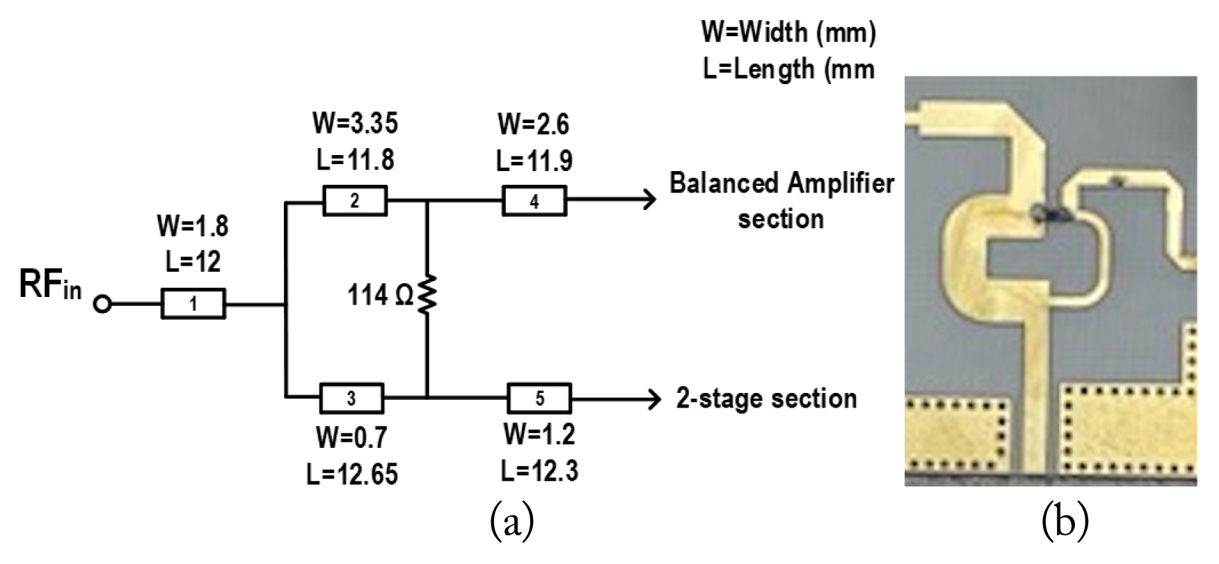
Beginning with the Wilkinson power splitter, an uneven splitter is specially designed to match the balanced amplifier with maximum gain. The optimum splitting ratio is empirically evaluated by electromagnetic simulation. A 35% split to the two-stage auxiliary device is found to achieve the target gain of 13 dB at both the balanced pair and the two-stage control auxiliary device across the 3.3–3.8 GHz band. Fig. 2 shows the schematic diagram in (a) and the photograph of the implemented unequal Wilkinson power splitter in (b).
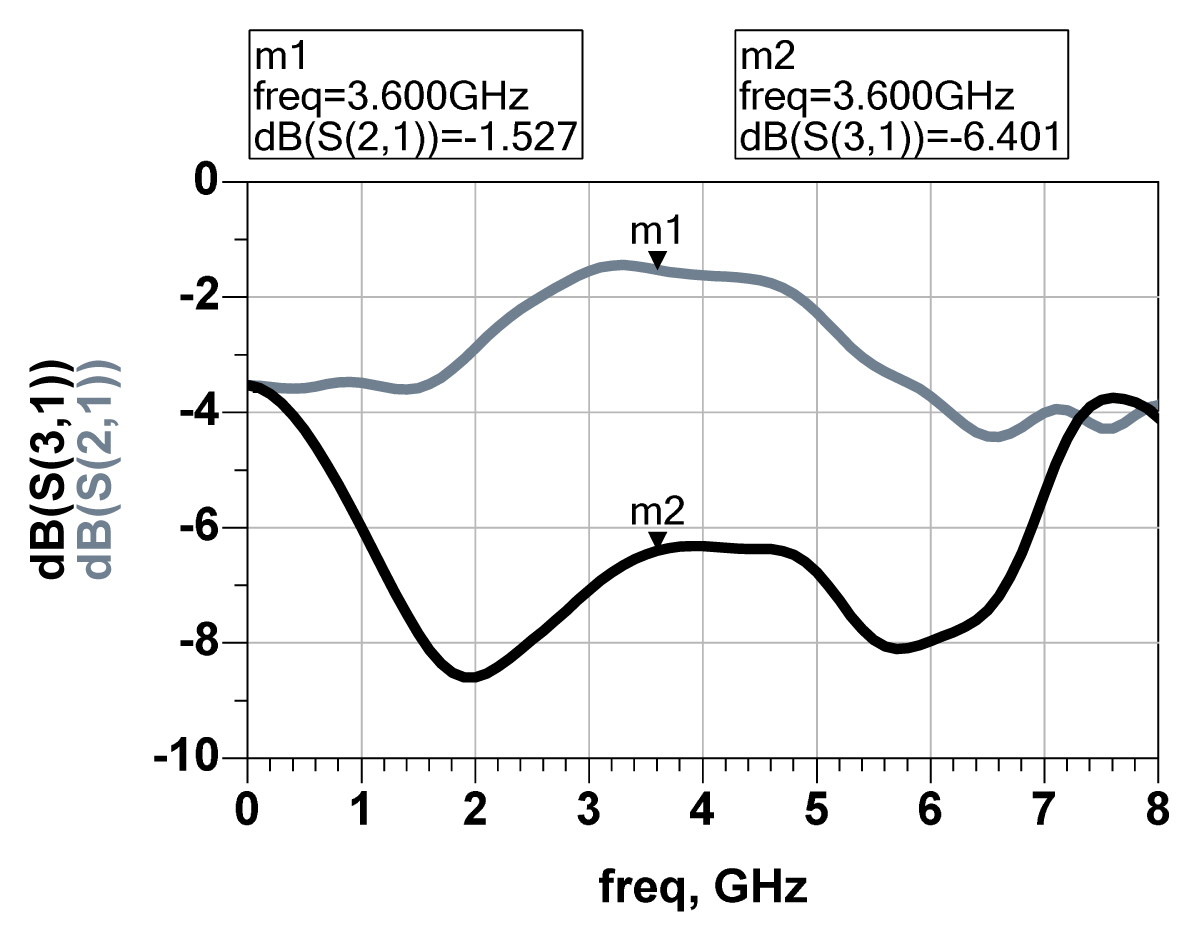
In Fig. 3, small signal power levels of −1.6 and −6.4 dB are fed to the balanced amplifier and the two-stage power amplifier respectively. After using the unequal Wilkinson splitter, the power to the balanced pair is split again using a 3 dB hybrid coupler.
At the output, a 3 dB hybrid coupler combines signals from the balanced pair and the two-stage control auxiliary device. As shown in Fig. 1, the device parasitics are well considered when designing the output matching networks. The balanced pair output matching network consists of two L-sections implemented in transmission lines. A standard
λ 4
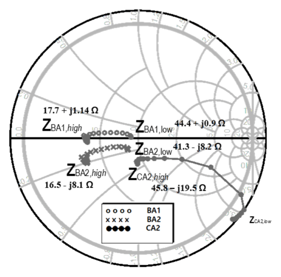
The following Smith chart illustrates the impedance trajectories at the current source planes describing the load modulation (Fig. 4).
To meet the target gain specifications, it is essential to have the input matching network appropriately designed with the output matching network already in place. Here, a Π-section is employed for both the balanced pair and the two-stage auxiliary device. However, the auxiliary device is tuned for optimal operation with maximum output gain considering that only 35% of the total input power is channeled to it. This proposal is implemented using similar active devices across the balanced pair and the two-stage auxiliary device, illustrating the similarities in structures of both input and output matching networks.
The proposed LMBA with a two-stage auxiliary device design begins with the selection of transistor devices. In this work, the CGH40006P device (Wolfspeed Inc., Durham, NC, USA) is selected and a transistor model is obtained to aid with the simulation design. Since the design is intended to be symmetrical, a low power device that can be experimentally analyzed is preferred. However, simulations with the second-generation CGH40010F device show insignificant performance variations.
With the transistor model in place, the resulting power contours are analyzed through load-pull simulations to establish the optimum impedance for maximum output power. Meanwhile, to deal with the packaged device parasitics, de-embedded data are utilized to obtain the optimal Ropt value helpful in configuring the output matching networks. The obtained load-pull data of the transistor model display an optimal resistance of 25 Ω while considering the intrinsic parasitic components of the device. Cree’s CGH40006P gallium nitride (GaN) high electron mobility transistor (HEMT) model is used to perform the load-pull simulations.
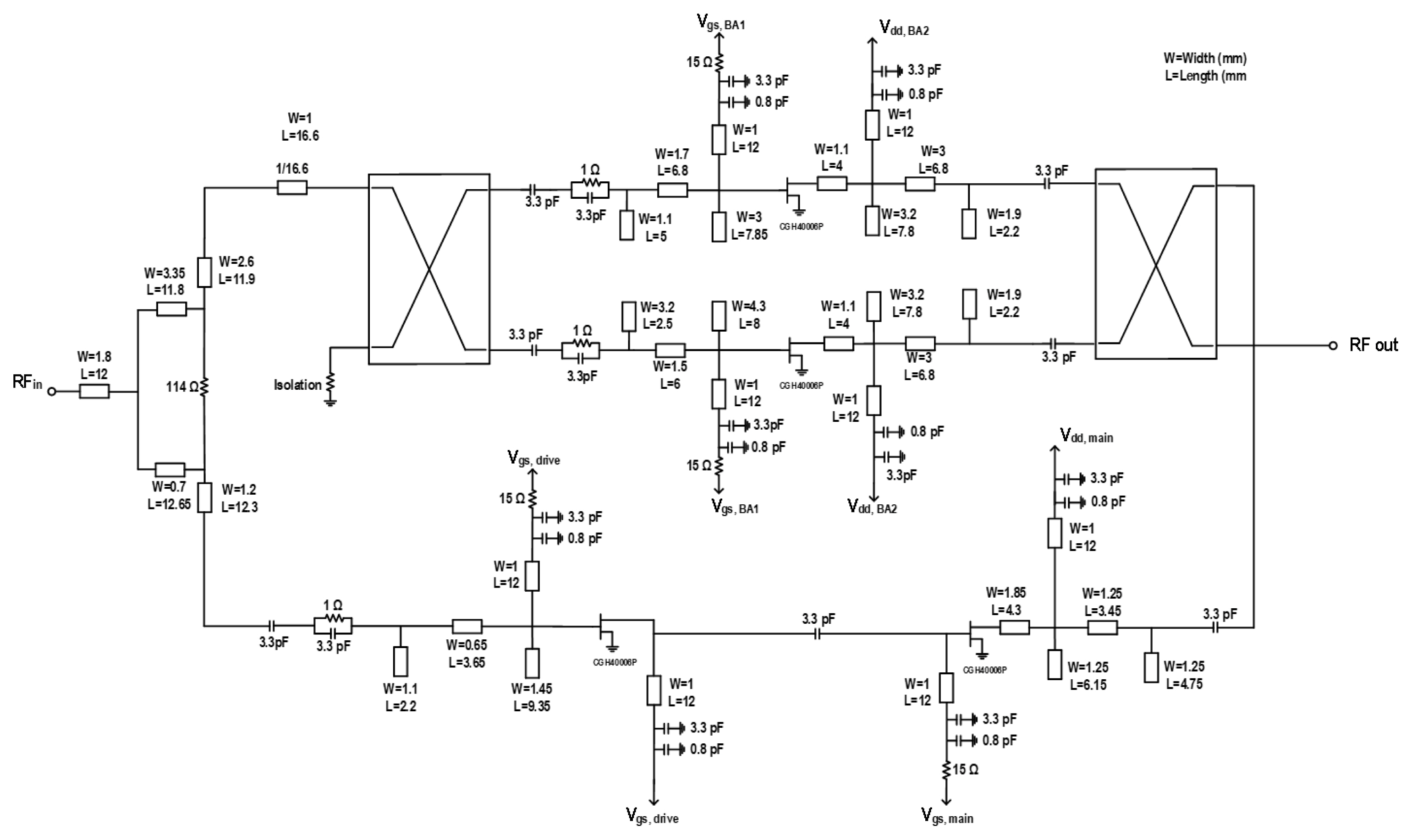
The full schematic of the designed power amplifier is shown in Fig. 5. The proposed LMBA with a two-stage control power amplifier is implemented on a 0.5 mm (20 mm)-thick Rogers 4350B printed circuit board (PCB) board with a dielectric constant of 3.48. A general design guideline can be summarized as follows:
1)Determine the design frequency band and target power requirements.
2)Based on (1), identify the appropriate devices for the balanced amplifier pair.
3)From load-pull analysis, find the optimum load impedances considering the intrinsic parasitic elements.
4)Design a 90° coupler for the target design frequency and the uneven Wilkinson power splitter for the target power split ratio.
5)Select devices for the two-stage control signal power.
6)Locate the optimal load for the two-stage control and design the interstage matching network.
7)Design the output matching networks according to the evaluated optimal impedances.
Design the input matching networks and the corresponding stabilization circuits.
III. Implementation and Measurements
The proposed LMBA is implemented on a Rogers 4003C substrate, and CGH4006P devices were used in both the balanced amplifier and two-stage control amplifier. Continuous wave (CW) measurements are performed with a single tone across 3.3–3.8 GHz. The measured gain remains above 10 dB in the low-power region and decreases slightly when approaching the high-power region. This observation is attributed to losses in the connectors, PCB, lumped components, and potential model inaccuracies in the turn-on phase of the Class C-biased two-stage auxiliary device. The imprecisely modeled turn-on state of the two-stage auxiliary device is a potential contributor to the varying measured and simulated performances. Similar observations have also been reported in previous works [6, 17, 18].
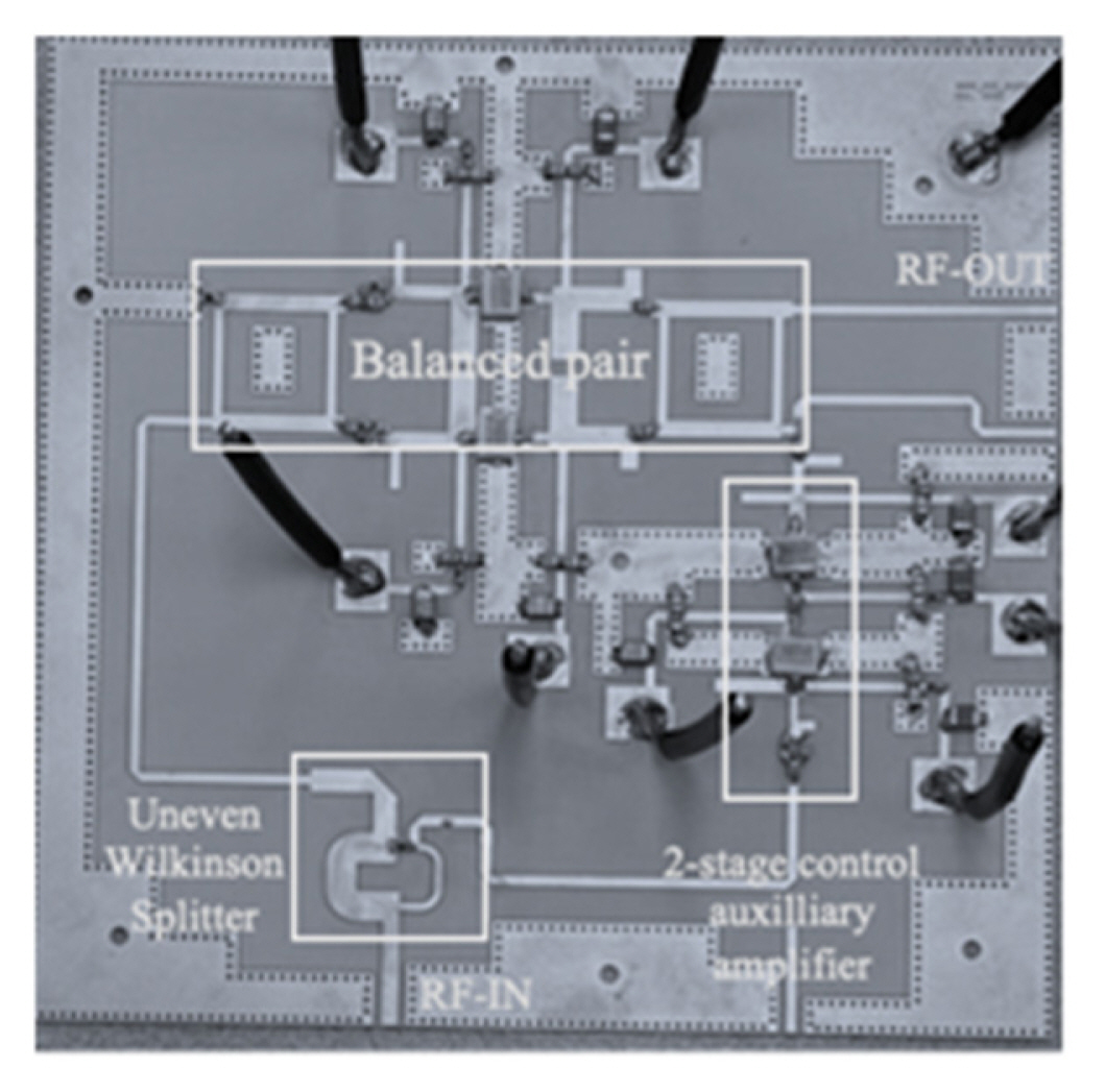
The fabricated LMBA with a two-stage control auxiliary amplifier is illustrated in Fig. 6. The PCB measures 11.3 cm × 11.55 cm. Both CW and wideband modulated signals are employed to perform measurements. The supply voltage of the balanced pair and control auxiliary is 28 V, and there is a quiescent current of 40 mA in each pair. The drive amplifier in the two-stage amplifier is adjusted to 22 V to ensure better linearity. The bias voltages for the balanced pair and the two-stage control auxiliary amplifier are −3 and −5 V, respectively. The S-parameter measured data are compared against the simulated data in Fig. 7.
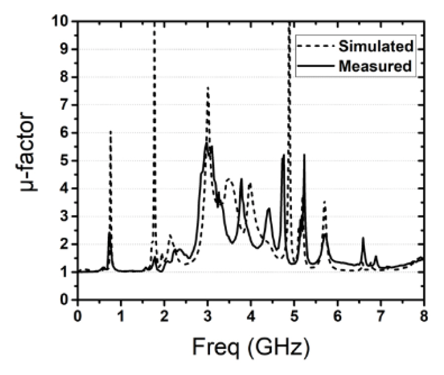
As already described, there is a pleasant consistency in the drain efficiencies of the measured and simulated data. Nonetheless, the gain performance, especially in the high-power region, indicates a slight drop. The measured stability characteristics of the implemented power amplifier are compared against the simulated data, as shown in Fig. 8. Unconditional stability is obtained across a broad frequency range with a μ-factor that is greater than 1.
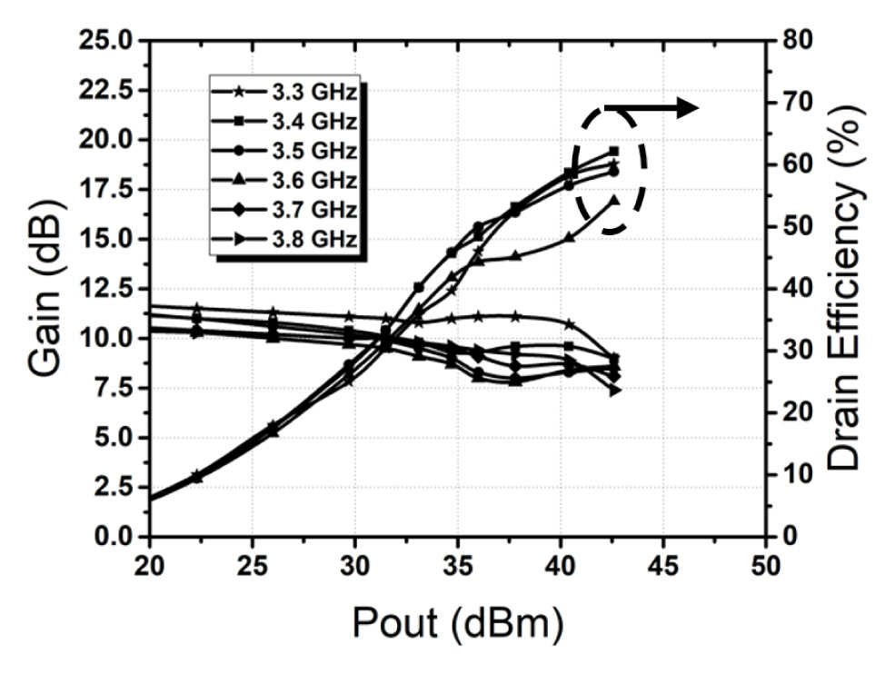
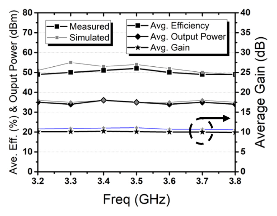
The frequency performance of the prototype is measured from 3.2 GHz to 3.8 GHz (Figs. 9, 10). The average gain, output power, and efficiency across the target frequency are summarized in Fig. 11. The peak drain efficiency is over 55% and above 45% within the target frequency band at 7.5 dB OBO. The values of gain performance in the low- and high-power regions measure above 10 and 7.5 dB, respectively. Performance comparison with previously published LMBAs of varying architectures are compared and summarized in Table 1 [3, 5, 7, 8, 10, 19–22].
IV. Conclusion
In this study, the LMBA has been modified as a two-stage control signal amplifier. The power contribution due to the additional amplifier on the control side provides for sufficient power in the high-power region operation of the power amplifier, resulting in a consistently high gain against the measured output power. This characteristic, along with the proper termination of the second harmonic, helps achieve the optimal load trajectories, thus allowing for high efficiency and good linearity tradeoff. In terms of input power utilization, the proposed topology is efficient as only less than 35% of the input power that is channeled to the auxiliary device is wasted. This is a direct consequence of the designed uneven Wilkinson power divider and happens when the auxiliary device is in the off state. At the target frequency of 3.3–3.8 GHz, the amplifier demonstrates a drain efficiency of 59%–64% at maximum output power and 46%–52% at 7.5 dB output back-off power.