A Folded Cascode CMOS Low Noise Amplifier with Transformer Feedback
Article information

Abstract
This study proposes a folded cascode CMOS low noise amplifier (LNA) with transformer feedback, implemented using a 0.13-μm CMOS process for wireless local area network front-end module applications. Compared to a conventional cascode inductive source degeneration LNA (ISDLNA), the folded cascode ISDLNA significantly improved the input-referred third-order intercept point (IIP3) as well as the 1-dB compression point (P1dB) by ensuring a large voltage headroom. Furthermore, the designed LNA also achieved a low noise figure (NF), while also saving the silicon area by magnetically coupling the source and folding inductors. When tested experimentally, the proposed LNA showed an S21 of 11.0 dB and an NF of 2.6 dB, while achieving an S11 of −7 dB at the operating frequency of 2.4 GHz. The measured input P1dB and IIP3 were −5.6 dBm and +2.5 dBm, respectively. The power dissipation was 9.6 mW from a 1.2-V supply voltage.
I. INTRODUCTION
Internet-of-Things (IoT) technologies connect devices, people, data, and processes across a wide range of applications, including healthcare, home automation, energy management, and environmental monitoring. Notably, the backbones of these highly reliable IoT systems are the various available wireless technologies (ZigBee, BLE, MBAN, and Wi-Fi). Among these, Wi-Fi has become a ubiquitous choice, as it supports an extremely diverse array of profiles while consuming varying levels of power and providing wide communication coverage. This is the consequence of the proliferation of its family of standards.
Since the 2.4-GHz ISM band is crowded by multiple strong sources of interference, such as cellular phones and CCTVs, Wi-Fi receivers need to be highly linear so as to minimize the degradation of the signal-to-noise-and-distortion ratio caused by inter-modulation, cross-modulation, saturation, and desensitization. In particular, the linearity burden in modern RF receivers pertains to the first building block of the low noise amplifier (LNA), since surface acoustic wave (SAW)-less techniques, such as the N-path filter from [1, 2], provide a high selectivity RF bandpass response with a very accurate center frequency set by the local oscillator, thus relaxing the linearity requirement of the subsequent building blocks (mixer, baseband analog chain, and analog-to-digital converter). Although various linearization techniques have been developed to improve the input-referred third-order intercept point (IIP3) of the LNA [3, 4], most are extremely sensitive to variations in process-temperature-voltage (PVT), and ultimately fail to improve large signal linearity, such as the input 1-dB compression point (P1dB) and blocker-induced noise figure (NF). In sum, an LNA with Wi-Fi applications should exhibit high input P1dB and IIP3 while maintaining a low NF of around 1 dB. This challenge becomes even more acute with the scaling down of the channel length of MOSFET devices due to the low supply voltage. In this paper, a folded cascode inductive source degeneration LNA (ISDLNA) with transformer feedback is proposed to simultaneously improve input P1dB and IIP3 without sacrificing NF performance and silicon area.
The remainder of this paper is structured as follows: Section II reviews conventional cascode and folded cascode ISDLNAs, while Section III presents an analysis of the input impedance, power gain, and NF of the proposed LNA. Following this, Section IV presents the design of the transformer and the completed LNA. The experimental results obtained on testing the proposed LNA are reported in Section V. Finally, Section VI presents the conclusions of this research.
II. REVIEW OF CONVENTIONAL CASCODE AND FOLDED CASCODE ISDLNAS
Fig. 1(a) depicts a conventional cascode ISDLNA used in a wide array of commercial narrowband receiver applications. These conventional ISDLNAs achieve excellent NF performance due to their simultaneous noise and input impedance matching. However, the relatively large voltage headroom used by the stacking topology of their common source (CS) and common gate (CG) transistors severely limits the output voltage swing under low supply voltage (VDD) conditions, resulting in poor input P1dB of the LNA. The drain-to-source dc bias voltage (VDS) of the CS and CG transistors in the cascode structure is approximately half of VDD, which means that the drain conductance (gds) nonlinearity of the CG transistor caused by the lower VDS can no longer be ignored. This causes additional IIP3 degradation. Additionally, as the operating frequency and gain increase, the CG stage limits the linearity of the LNA due to parasitic junction capacitance, including the drain-to-source capacitance of the CS transistor, gate-to-source capacitance, and the finite output resistance of the CG transistor [5].
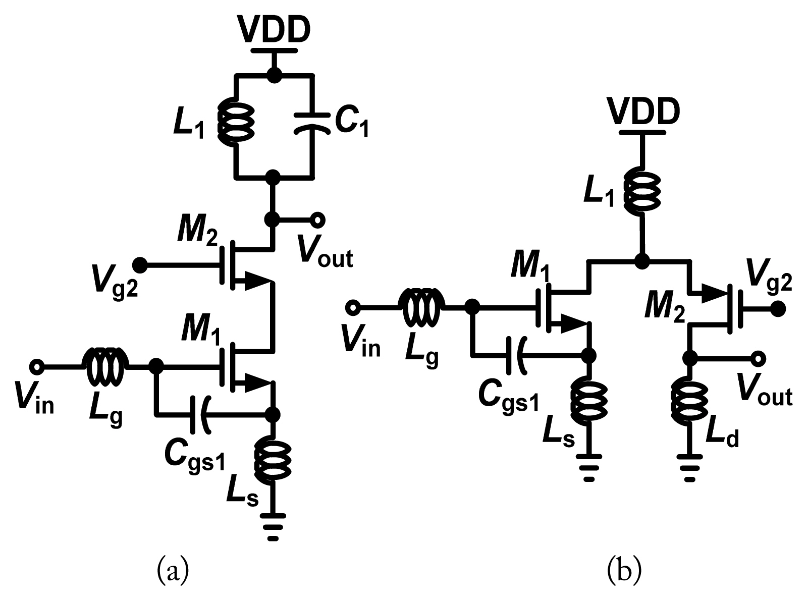
Schematics of (a) conventional cascode inductive source degenerated LNA (ISDLNA) and (b) folded cascode ISDLNA.
To overcome the drawbacks of the conventional cascode ISDLNA, a folded cascode ISDLNA, as depicted in Fig. 1(b), was reported in [6, 7]. The VDS of all transistors was set close to VDD due to the absence of the stacking gain stage (CG transistor), enabling the folded cascode ISDLNA to achieve exclusive advantages in terms of P1dB and IIP3. Furthermore, since a PMOS transistor typically exhibits higher output resistance than an NMOS transistor under the same channel length conditions, this mitigates the IIP3 degradation caused by the gds nonlinearity of the CG transistor. Some improvement in IIP3 can also be achieved through distortion cancellation by controlling the size and dc bias voltage of the CG transistor and canceling out the nonlinearities of the NMOS and PMOS transistors [8]. However, such an LNA requires a larger silicon area than a conventional cascode ISDLNA, owing to the inclusion of a folding inductor that operates as an RF choke.
III. ANALYSIS OF THE PROPOSED FOLDED CASCODE ISDLNA WITH TRANSFORMER FEEDBACK
Fig. 2 presents the proposed folded cascode ISDLNA with transformer feedback. An external matching network composed of two off-chip inductors (Lp and Lg), was adopted to achieve simultaneous noise and input impedance matching with minimal signal loss. To reduce the silicon area occupied by the onchip inductors, the transformer feedback was implemented by introducing magnetic coupling between the source inductor (Ls) and the folding inductor (L1), representing the primary and secondary coils of the transformer, respectively. These two coils had the same polarity, allowing them to form negative feedback. This transformer feedback effectively cancelled the Miller capacitance (gate-to-drain capacitance [Cgd]), neutralized the amplifier, and improved the linearity. In contrast to conventional resistive feedback or active feedback LNAs, in which the feedback network directly degrades the overall NF of the LNA, the proposed transformer feedback LNA minimized the NF degradation caused by the feedback network due to the realization of noiseless feedback between the two existing inductors. However, this transformer feedback requires detailed analysis regarding the effect of the qualify factor (Q-factor) and the coupling coefficient of the on-chip transformer on the input impedance (Zin), power gain (S21), and NF of the amplifier.
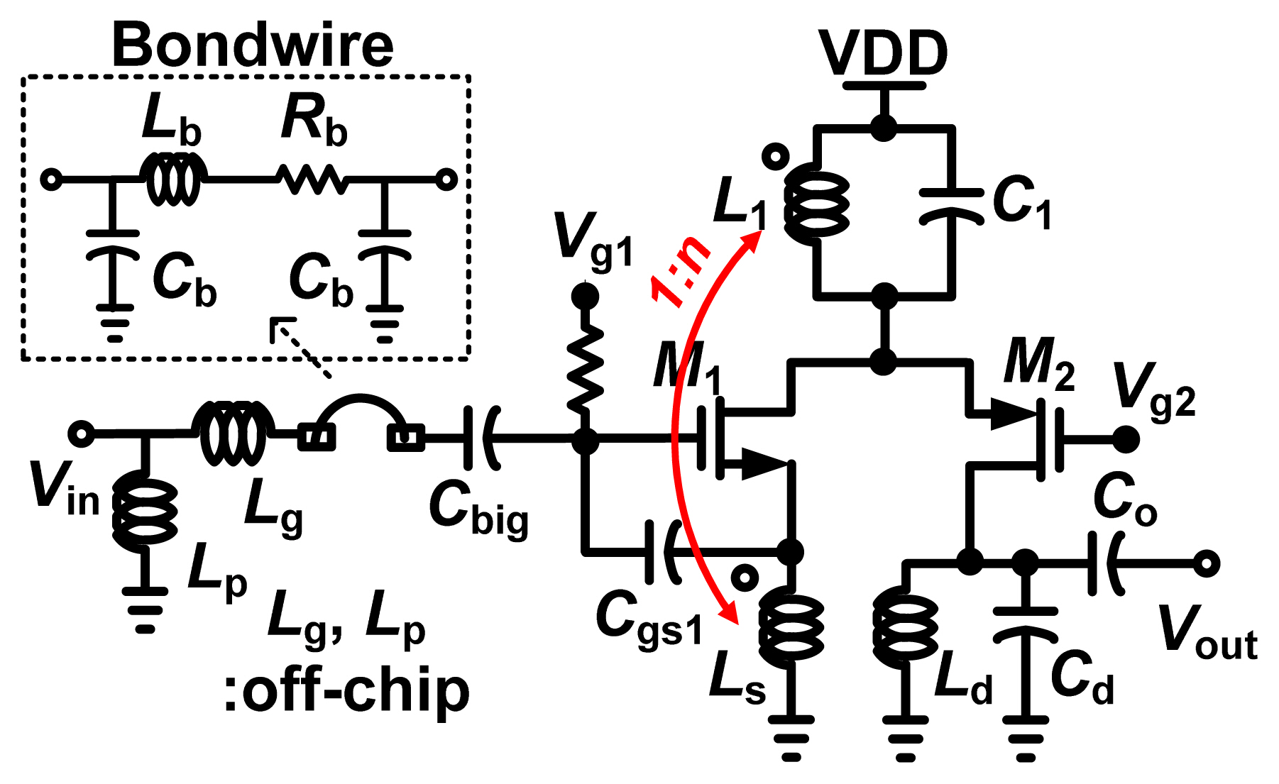
Schematic of the proposed folded cascode ISDLNA with transformer feedback. The channel length of all MOSFETs is 130-nm. The gate-to-source capacitance (Cgs1) is the sum of the intrinsic Cgs1 and any extra added capacitance. The capacitance C1 includes all node-to-substrate parasitic capacitances caused by MOSFETs as well as any extra added capacitance. The capacitance Cbig is an ac-coupling capacitor.
1. Input Impedance
Fig. 3 presents a small-signal equivalent circuit model of the proposed LNA, where i1 and i2 denote the alternating current (ac) flowing into the primary and secondary coils, respectively. Meanwhile, the effect of the transformer’s magnetic coupling is modeled as two current sources. The transformer turn ratio and coupling coefficient are denoted by n and k, respectively. Considering that the parallel L1//C1 circuit resonates at the operating frequency (ω0), the approximate Zin of the proposed LNA is calculated as follows:
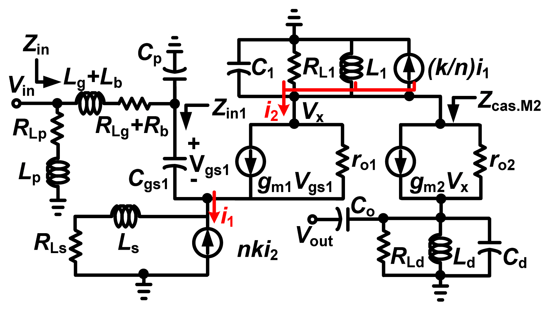
Small-signal equivalent circuit model of the proposed folded cascode ISDLNA with transformer feedback. The RLp, RLg, RLs, RL1, and RLd denote the series or parallel resistances resulting from the finite Q-factor of the inductors.
where gm1 and gm2 represent the transconductances of M1 and M2, respectively. Furthermore, ro1 and ro2 denote the output resistances of M1 and M2, while Zin1 and Zcas.M2 are the impedances looking into the gate node of M1 and the source node of M2 at the operating frequency, respectively. Meanwhile, Rd indicates the effective resistance of RLd and Rs/(ω0CoRs)2 in parallel, and Cp includes the effect of the Miller capacitance (Cgd1) of M1. The effect of the bond wire is also considered for calculating the Zin. Similar to the conventional cascode ISDLNA presented in Fig. 1(a), the real and imaginary parts of the Zin of the proposed LNA can be independently tuned by Lp, Lg, and Ls. The reactive parts were canceled at ω0, while the real part was set equal to the source resistance (Rs) for input impedance matching. In this design, considering the variations in Zin1, an input impedance matching network composed of Lp and Lg was designed to achieve an input return loss (S11) of less than −10 dB with a low NF across a wide range of k, as shown in Fig. 4.

Calculated input return loss (S11), S21, and NF of the proposed LNA according to variations of k of the transformer. The design parameters extracted from the foundry’s process design kit were used for this calculation.
2. Power Gain
When the reactive part of Zin is perfectly canceled at ω0 and the parallel L1//C1 and Ld//Cd//Co circuits resonate at ω0, the power gain (S21) of the proposed LNA at ω0 can be approximately calculated as (2). Furthermore, as shown in Fig. 4, increasing the value of k helps achieve a higher S21 and smaller chip area.
3. Noise Figure
Under the same conditions for the calculation of S21, the NF of the proposed LNA at ω0 can be approximately calculated as (3), where γn represents the bias-dependent channel thermal noise coefficient of MOSFET Mn and QLs is the quality factor (Q-factor) of the primary coil. Fig. 4 presents the calculated NF of the proposed LNA according to variations in k. The design parameter values of the small-signal equivalent circuit model listed in Fig. 4 were used in this calculation. Based on the electromagnetic (EM) simulation, the practical design parameter values of the on-chip transformer were also reflected in the calculation.
In the case of conventional folded cascode LNA employing transformer feedback reported in [9], a reasonably large variation in gain over the coupling coefficient (k) has been observed. As the value of k increased, its gain was severely degraded, while its NF was slightly improved. Unfortunately, the value of k was set at 0.1 to avoid a severe gain drop in the LNA, thus sacrificing the advantage of size reduction through transformer coupling. However, in the case of the proposed LNA, the variations in its gain and NF over k were quite small. Its gain was improved as the value of k increased, with the NF variation being approximately 0.1 dB when k was changed from 0.3 to 1. As a result, in contrast to the conventional LNA, it is desirable to increase the value of k to reduce the chip size. Drawing on this aspect, this work attempted to increase the value of k to achieve a higher S21 and smaller chip area.
IV. DESIGN OF THE TRANSFORMER AND THE COMPLETED LNA
Fig. 5 shows the physical layout of the designed transformer. To achieve a high Q-factor, ultra-thick metal (UTM) provided by the adopted process technology was used. The transformer was designed to have an n of 2 and k of 0.8 to optimize its key performances, such as Zin, S21, and NF. The line width was 9- μm, the space between lines was 3-μm, and the inner radius was 290-μm. The number of turns in the primary and secondary coils was 2 and 4, respectively. Fig. 6 presents the EM simulation results (inductance, Q-factor, and coupling coefficient) of the designed transformer, which was simulated using a 3D High-Frequency Simulation Software (HFSS) simulation tool. The thickness and resistivity of the handle wafer were 700 μm and 1 kΩ·cm, respectively. The UTM was made of aluminum (Al), and its thickness was 4.1 μm. At an operating frequency of 2.4 GHz, the inductance and Q-factor of the primary coil (secondary coil) were approximately 0.9 nH and 2.4 (3.2 nH and 2.4). The simulated k was about 0.89 at an operating frequency of 2.4 GHz.
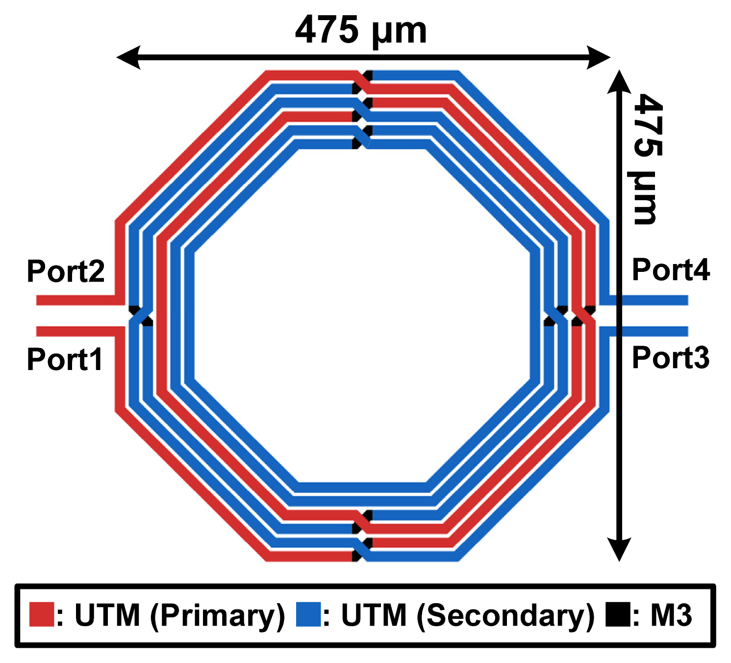
Physical layout of the designed transformer.

Electromagnetic simulation results of the designed transformer: (a) inductance, Q-factor, and (b) coupling coefficient.
Fig. 7 presents the pre-layout simulation results, post-layout simulation results, and calculation results of the completed LNA. Notably, the post-layout simulation included the effects of input/output (I/O) pads and electrostatic discharge (ESD) diodes. The designed LNA exhibits pre-layout simulated S21, S11, and NF values of 19.5 dB, −10.7 dB, and 1.2 dB, and post-layout simulated S21, S11, and NF values of 16.5 dB, −9.5 dB, and 1.4 dB, respectively. It is further observed that the pre-layout simulation results, which excluded the IO pads, ESD diodes, and parasitic components of the metal wires are well matched with the calculation results.
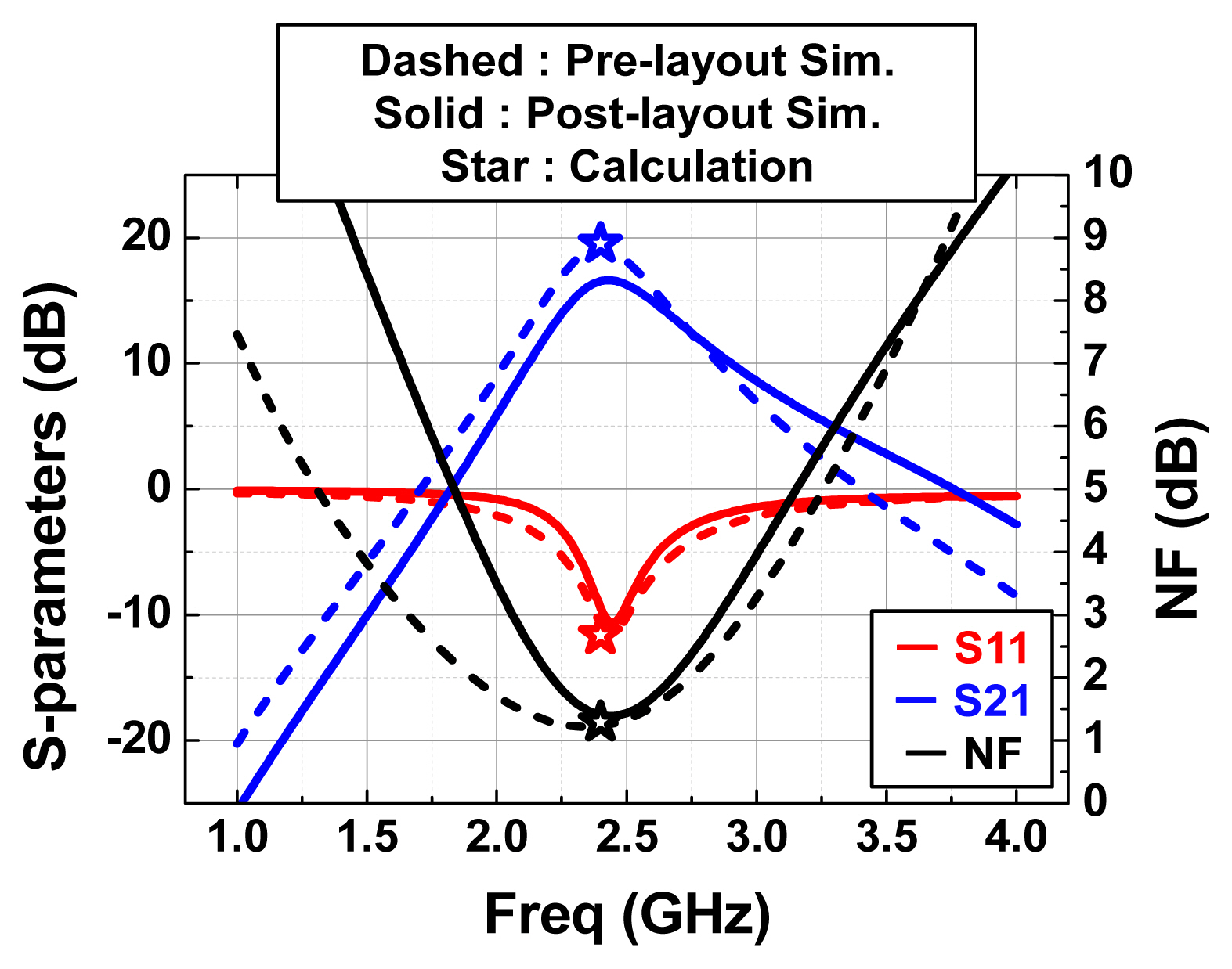
Pre-layout simulation results, post-layout simulation results, and calculation results of the completed LNA.
V. EXPERIMENTAL RESULTS
The proposed folded cascode ISDLNA with transformer feedback was implemented using a DB HiTek 0.13-μm RF CMOS process. Fig. 8 shows photographs of the conventional cascode ISDLNA from Fig. 1(a) and the proposed LNA from Fig. 2. The conventional cascode ISDLNA was implemented using the same process technology so as to directly compare its performance to that of the proposed LNA. Excluding the IO pads, the chip areas of the conventional cascode ISDLNA and the proposed LNA were approximately 0.2 mm2 and 0.3 mm2, respectively.
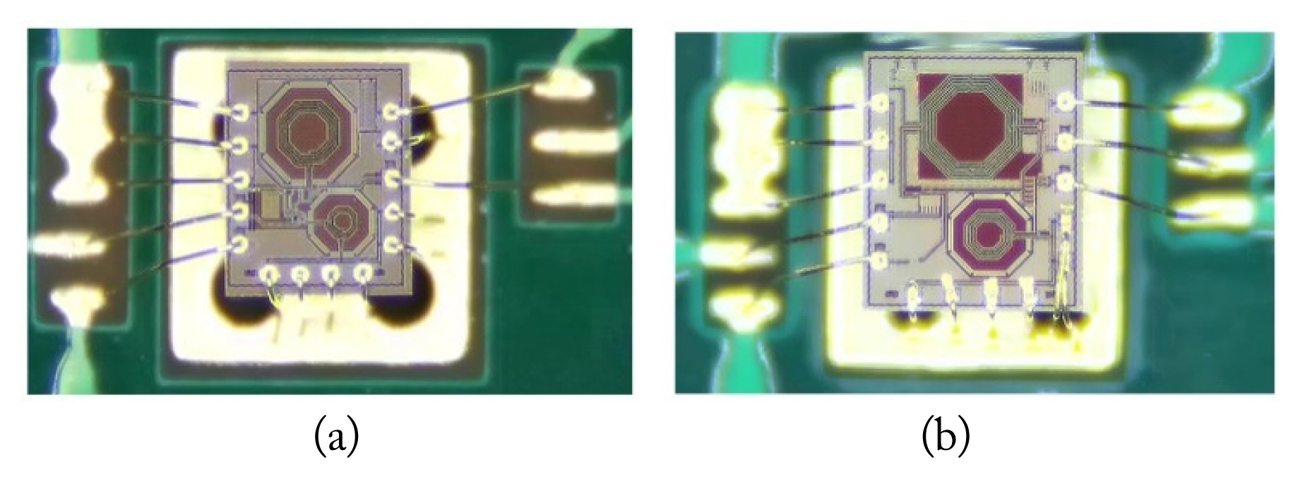
Photographs of the implemented chips: (a) conventional cascode ISDLNA illustrated in Fig. 1(a); and (b) the proposed LNA presented in Fig. 2.
Fig. 9 presents the measured S-parameters, NF, IIP3, and input P1dB of both LNAs. To ensure a fair comparison, the power consumption of both LNAs was set at 9.6 mW, drawn from a 1.2-V supply voltage. The two-tone spacing for the measurement of IIP3 was 10 MHz. The conventional cascode ISDLNA showed an S21 of 15.7 dB, an NF of 1.1 dB, an IIP3 of −8.5 dBm, an output-referred third-order intercept point (OIP3) of +7.2 dBm, and an input P1dB of −14 dBm, while achieving an S11 of less than −10 dB at an operating frequency of 2.4 GHz. In contrast, the proposed LNA exhibited an S21 of 11.0 dB, an NF of 2.6 dB, an IIP3 of +2.5 dBm, an OIP3 of +13.5 dBm, and an input P1dB of −5.6 dBm while achieving an S11 of −7 dB at the operating frequency of 2.4 GHz. As predicted, the proposed LNA significantly improved OIP3 and input P1dB with nearly the same power consumption and chip area compared to the conventional cascode ISDLNA. These results may be attributed to the inherently high linearity characteristic of the folded cascode topology. In addition, considering the simulated OIP3 of the folded cascode LNAs obtained with and without the transformer feedback, an additional OIP3 improvement of about 2 dB was observed when using the transformer feedback. Unfortunately, a peak gain degradation of 6 dB and an average NF degradation of 1.1 dB were observed in the experimental measurements which were not seen in the post-layout simulation. The main reason for this degradation could be the shifted resonance frequency of L1 and C1 from 2.4 GHz, resulting from an inaccurate EM simulation of the transformer.
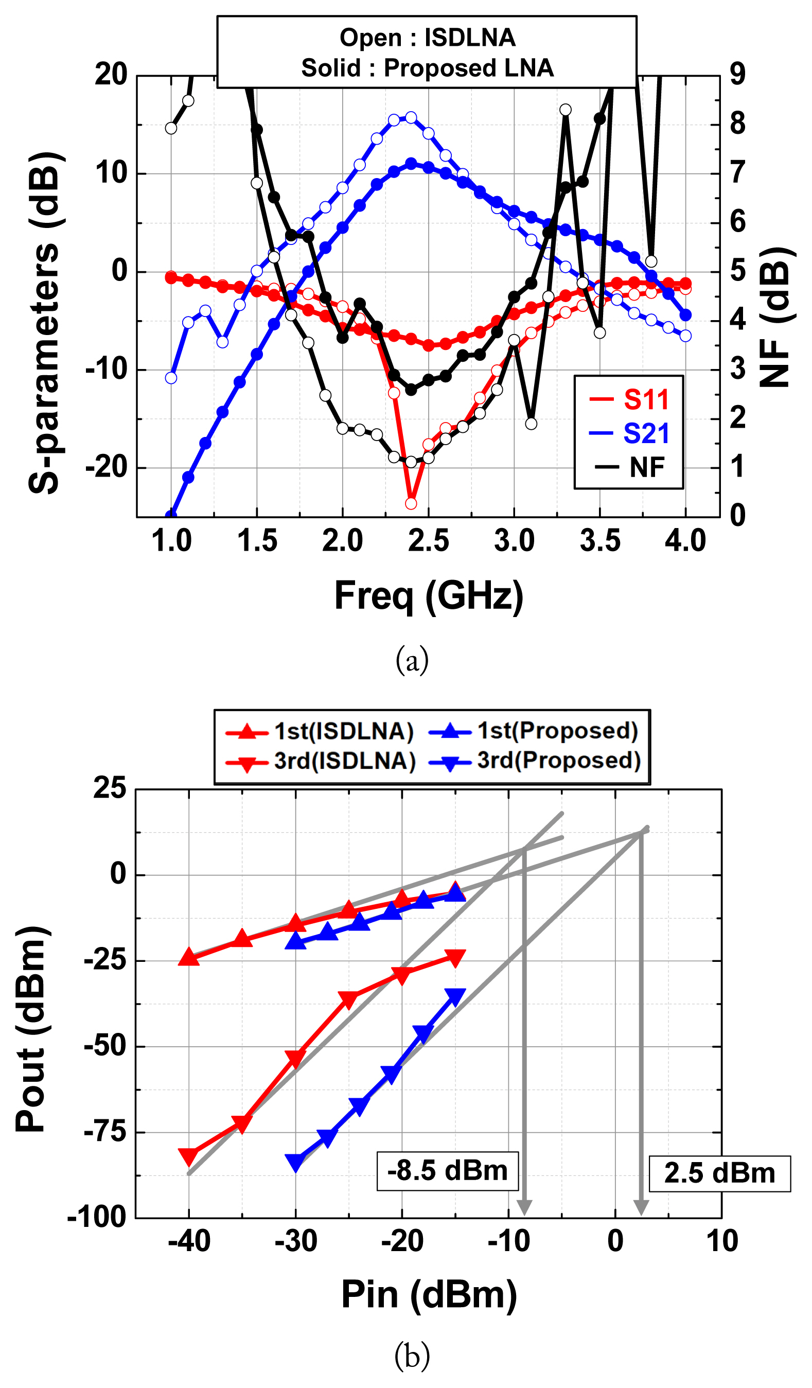
Measured RF performances of the conventional cascode ISDLNA and the proposed LNA: (a) S-parameters, NF, and (b) IIP3.
Table 1 compares the performance of the proposed LNA to that reported in previous works [10–14]. The figure-of-merit (FoM) is derived in accordance with [15], as follows:

Performance summary and comparison
where Pdc refers to dc power dissipation. Compared to previous works, including the conventional cascode ISDLNA, the proposed LNA achieves a higher OIP3 and input P1dB with comparable NF performance due to its folded cascode topology and the transformer feedback. Moreover, the silicon area occupied by the proposed LNA is nearly identical to that used by the conventional cascode ISDLNA.
VI. CONCLUSION
A folded cascode CMOS LNA with transformer feedback was proposed for use in wireless local area network front-end module applications. Compared to previous works, including a conventional cascode ISDLNA, the proposed LNA significantly improved the IIP3 and input P1dB with exhibiting a somewhat degraded NF, while also saving silicon area by magnetically coupling the source and folding inductors. In terms of experimental results, the proposed LNA exhibited an S21 of 11.0 dB, an NF of 2.6 dB, an IIP3 of +2.5 dBm, an OIP3 of +13.5 dBm, and an input P1dB of −5.6 dBm while also achieving an S11 of −7 dB at the operating frequency of 2.4 GHz. The power consumption was 9.6 mW from a 1.2-V supply voltage.
ACKNOWLEDGMENTS
This work was supported by a grant from the National Research Foundation of Korea (NRF), funded by the Korean government (MSIT) (No. 2021R1A4A1032234), and by a grant from the National Research Foundation of Korea (NRF), also funded by the Korean government (MSIT) (No. 2022R1A2C2011267). The EDA tool was supported by the IC Design Education Center (IDEC), Korea.
References
Biography

Dongmyeong Kim, https://orcid.org/0000-0002-9830-4664 received his B.S. and M.S. degrees in electronic engineering from Jeonbuk National University, Jeonju, Korea, in 2019 and 2021, respectively. He is currently working toward a Ph.D. degree in electronic engineering at Jeonbuk National University. His doctoral research focuses on RF front-end circuit designs, such as highly linear sub-1dB NF low noise amplifiers and reconfigurable power amplifiers in CMOS.

Haseon Song, https://orcid.org/0009-0006-8525-7164 received his B.S. and M.S. degrees in electronic engineering from Jeonbuk National University, Jeonju, Korea, in 2021 and 2023, respectively. His research during M.S. course was focused on highly linear low noise tunable poly-phase filters and image rejection mixers for wideband and fast spectrum sensing applications.

Ilku Nam, https://orcid.org/0000-0001-7326-2253 received the B.S. degree in electronics engineering from Yonsei University, in Seoul, Korea, in 1999 and the M.S. and Ph.D. degrees in Electrical Engineering and Computer Science from Korea Advanced Institute of Science and Technology (KAIST), in Daejeon, Korea, in 2001 and 2005, respectively. His Ph.D. work at KAIST was related to low-power CMOS RF transceiver integrated circuits (IC) design for low-power IoT applications. From 2005 to 2007, he was a senior engineer with RF development team, Samsung Electronics, Korea, where he was involved in developing world first multistandard multiband mobile digital TV tuner ICs supporting DVB-H/T, T-DMB, and ISDB-T/H. In 2007, he joined the Department of Electrical and Electronics Engineering, Pusan National University, Busan, Korea, where he was involved in the design of the 60 GHz WiGig circuits. His research interests include CMOS RF/mmWave/analog integrated circuits and RF security system for wireless communications, such as IoT and 5G mobile systems.

Donggu Im, https://orcid.org/0000-0003-2892-6254 received the B.S., M.S., and Ph.D. degrees in electrical engineering and computer science from the Korea Advanced Institute of Science and Technology (KAIST), Daejeon, Korea, in 2004, 2006, and 2012, respectively. His doctoral research focused on integrated RF front-ends with antenna switch, power amplifier, directional coupler with transmitter leakage suppression, and tunable impedance matching circuit in silicon-on-insulator (SOI) CMOS. From 2006 to 2009, he was an Associate Research Engineer with LG Electronics, Seoul, Korea, where he was involved in the development of universal analog and digital TV receiver ICs. From 2012 to 2013, he was a Post-Doctoral Researcher with KAIST, where he was involved in the development of the first RF SOI CMOS technology in Korea with SOI business team in National NanoFab Center (NNFC), Daejeon, Korea, and was responsible for the design of antenna switch, digitally tunable capacitor, power MOSFETs, and ESD devices. In 2013, he joined the Texas Analog Center of Excellence (TxACE), Department of Electrical Engineering, University of Texas at Dallas, as a Research Associate, where he developed ultra-low-power CMOS radios with adaptive impedance tuning circuits. In 2014, he joined the Division of Electronic Engineering, Jeonbuk National University, Jeonju, Korea, and is now an associate professor. His research interests are CMOS analog/RF/mm-wave ICs and system design for wireless communications. Dr. Im was the recipient of the Bronze Prize in the 18th Human-Tech Paper Awards from Samsung Electronics, Korea, in 2011.