An Effective Experimental Optimization Method for Wireless Power Transfer System Design Using Frequency Domain Measurement
Article information
Abstract
This paper proposes an experimental optimization method for a wireless power transfer (WPT) system. The power transfer characteristics of a WPT system with arbitrary loads and various types of coupling and compensation networks can be extracted by frequency domain measurements. The various performance parameters of the WPT system, such as input real/imaginary/apparent power, power factor, efficiency, output power and voltage gain, can be accurately extracted in a frequency domain by a single passive measurement. Subsequently, the design parameters can be efficiently tuned by separating the overall design steps into two parts. The extracted performance parameters of the WPT system were validated with time-domain experiments.
I. Introduction
Wireless power transfer (WPT) technology has undergone remarkable developments in recent years, which has enhanced the convenience and mobility of electronic devices. WPT technology can be applied to many applications such as biomedical applications [1, 2], mobile phones [3], electric vehicles, and battery charging systems [4, 5].
Today, WPT research has mainly focused on magnetic resonance and inductive coupling methods because of their high efficiency and simplicity. The magnetic resonance method using four coils has an operating frequency of several MHz and can transfer energy across a midrange distance due to the high quality factors (Q-factors) of the coils [6, 7]. Since high frequency operation at several MHz causes critical switching loss in semiconductor devices for high-power applications, the magnetic resonance method is appropriate for low-power applications across a midrange distance.
Meanwhile, the inductively coupled WPT method operating at a low frequency below 1 MHz is basically similar to the coupling of a transformer in typical resonant power converters, although the coupling coefficient in the WPT is much lower [8]. By employing a proper compensation network, the inductively coupled WPT shows quite high power transfer efficiency at short distances. However, the efficiency decreases rapidly when the distance between the two coils is increased; therefore, this method is more suitable for high-power applications at relatively close distances.
Due to the low coupling coefficient between the coils in the inductive coupling WPT system, the leakage inductance of the coils is larger than the magnetizing inductance, resulting in a large input reactance. To reduce the input imaginary power and increase the power transfer efficiency, effective compensation topologies have been introduced and analyzed in [9]. In addition, many researchers have made significant contributions in different areas, such as with a high-efficiency power source [10, 11], analysis and modeling of coupling systems, [12–14], and optimal load [15, 16].
Most WPT research utilizes full-wave simulation tools to characterize self-inductance and mutual inductance of the coils and to construct the circuit model. The WPT system, which includes coils and an impedance compensation network, is then simulated in a circuit solver, such as SPICE, prior to experiments with a power source [17]. Since most WPT systems are very sensitive to the impedance matching condition and operating frequency, the parasitic components in the impedance matching network and manufactured coils should be accurately characterized to achieve an exact operational target. Although full-wave simulations are quite time-consuming, the simulated results of the coil characteristics and resultant WPT system performances can still differ from actual measured results due to discrepancies between modeling and manufacturing. In addition, after the WPT system is modeled in a circuit fashion using the full-wave simulation results, it is difficult to consider the frequency-dependent variations of inductances and the parasitic resistances of coils caused by the skin effect and the proximity effect of wires. It is also difficult to characterize parasitic stray inductances or contact resistances in the printed circuit board (PCB) layout and assembly.
In this paper, a new experimental optimization method for WPT systems based on frequency domain measurements is proposed. Various power transfer characteristics can be extracted with one passive measurement by considering the overall parasitic components in the compensation networks, the coils, and even the PCBs. From the extracted performance parameters of the designed WPT system, the real WPT operation can be efficiently optimized in a frequency domain.
To demonstrate the proposed design method, the previous design flow of a WPT system is summarized in Section II, and the experimental optimization method is proposed in Section III. Section IV shows the design example of the WPT system to demonstrate the proposed design flow. In Section V, the performance parameters of the designed WPT system are extracted and validated with time-domain experiments, including implementation of a DC-AC inverter. Conclusions are drawn in Section VI. The major contributions of the proposed design method are summarized as follows: (1) the operating conditions of a WPT system can be efficiently optimized based on various performance parameters extracted by frequency domain measurements; (2) unexpected parasitic components can be considered in the frequency domain measurements, and the extracted performance parameters are very accurate; and (3) the performance of AC-AC stages, including the coils and compensation networks, can be separately characterized, before the power source and rectifier are implemented. Therefore, the design parameters can be tuned much more efficiently.
II. Previous Design Flow for a WPT System
The design method of a WPT system has been introduced in several research studies such as [5], in which optimal topologies and device parameters were analyzed by mathematical calculations or simulations. In this paper, rather than the design method of a specific WPT topology or a coil, the overall design flow to implement a general WPT system is considered. Additionally, the focus here is a WPT system for high-power applications, which employs a DC-AC inverter in front of the AC input stage.
Fig. 1 describes a previous typical design process to implement a WPT system. First, the design target is specified in Step 1. In Step 2, the proper types of coils and compensation networks are selected. Then, the structure and geometry are designed using the corresponding analytical expressions. Full-wave simulations can also be performed to design coils of arbitrary shapes, including ferrite shields or metal chassis. The various performance parameters of power transfer characteristics are analytically derived from the WPT circuit models in [17]. WPT performance can be predicted in the design stage prior to manufacturing. The optimal operating frequency ωo and AC input voltage V1 for specific load conditions can also be determined by calculations or simulations.
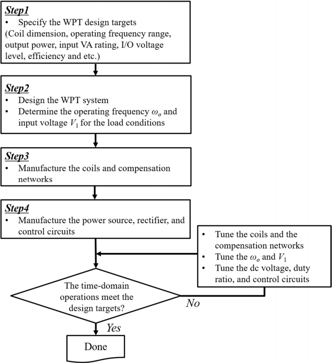
Previous typical design process of a WPT system.
Step 3 and Step 4 are manufacturing processes to implement the designed WPT system. Passive coils and compensation networks are implemented in Step 3, and the power source with active devices is implemented in Step 4. The rectifier is also implemented to obtain DC output voltage, if necessary. If the experimental tests of the WPT performances are well matched with the desired target performance, the design of the WPT system has been successfully completed.
In most cases, however, the performance of the implemented WPT system is quite different from the desired performance due to unexpected errors and parasitic components in the devices. Device parameters and coil geometries have specific tolerances. Thus, production errors can cause significant mismatches of the operating targets, since the operation of most WPT systems is very sensitive in terms of maintaining a high Q-factor. Therefore, device parameters and coils should be accurately tuned and debugged to achieve the desired performance, which requires several repeated efforts, as indicated by the feedback loop in the design flow of Fig. 1.
Tuning of the coils and compensation networks is usually performed, and the operating frequency ωo or AC input voltage V1 can also be adjusted. The design parameters of the power source, such as the DC input voltage, duty ratio, and gate-driving control circuits, are also adjusted to obtain the desired AC voltage level. As a result, the various design parameters in the WPT system, including coils, compensation networks, the power source, and even the rectifier, should all be tuned and debugged in the final step. Hence, finding the root causes of the discrepancies between the design targets and the achieved experimental results is quite challenging, and a high level of engineering experience and iteration techniques are required to achieve the desired performance of a WPT system.
III. Proposed Design Flow for a WPT System
This section proposes an experimental optimization method for WPT systems prior to the implementation of a power source or rectifier. The formulation and the new design flow are proposed herein. Using the proposed method, the tuning and debugging process of a WPT system should be much easier and more effective.
1. Formulation of WPT Performance Parameters with Impedance Parameters in a Frequency Domain
Many WPT research projects have employed frequency domain measurement to estimate the efficiency, output power, or voltage gain of a WPT coupling network in a frequency domain [18, 19]. However, the source and load impedances are usually assumed as 50 Ω to be matched with the characteristic impedance of the instruments and cables. Especially for high-power applications, a source impedance of 50 Ω is far different from the impedance of a real power source, which is predominantly determined by the on-switching resistance in the inverter and is usually below several ohms. A larger source impedance can significantly degrade power transfer efficiency and can also cause heat problems. Load impedance can also be different from 50 Ω and freely changed from several ohms to hundreds of ohms, depending on the end-side DC-DC converter and battery condition [15].
In [18], external impedance transformation circuits were employed to change the load conditions for frequency domain measurement. However, the external circuits cause additional parasitic components and efficiency degradation in practical implementations.
The performance parameters of power transfer characteristics for an arbitrary source and load impedances are formulated using the impedance (Z)–parameters herein. Fig. 2 shows the overall WPT system from a DC power source to an output load. The DC voltage Vdc is supplied by a DC voltage supply or an AC-DC converter with a DC-link capacitor, Cdc. ZL represents the impedance of the rectifier and output load. Since the frequency domain formulations are intended to analyze the AC-AC characteristics of the WPT system, Port 1 is located at the AC input stage after the DC-AC inverter, and Port 2 is located at the AC output stage before the rectifier, as depicted in Fig. 2. Also, in the frequency domain analysis, the DC-AC inverter side should be disconnected, so that V1 and I1 at Port 1 represent the AC driving voltage and current. In the conventional frequency-domain characterization method, only the WPT coils and compensation networks are characterized as a two-port network. The load is separately characterized by additional measurements and combined with the two-port network to investigate the whole performance of the WPT system. However, the separate measurements should increase the overall errors in predicting the performance parameters. In this paper, the performance parameters are derived by a measurement with the load also connected, which can include all parasitic stray inductances or contact resistances in the PCB layout and assembly. This can significantly increase the accuracy in the frequency-domain characterization.
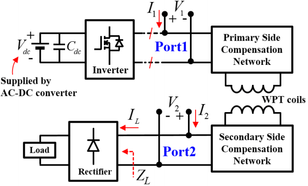
Configuration of WPT system from DC power source to arbitrary load.
The WPT performance parameters from the AC driving side to the load can then be expressed by impedance parameters between the two ports. First, the input real power Pin, imaginary power Qin, and apparent power Sin are expressed as:
where Yin|I2=0 represents the input admittance at Port 1 when I2 is zero, which is identical to the inverse of the Z11 parameter. V1 is also a complex number representing the magnitude and phase of the input sinusoidal voltage. Actually, the AC voltage from the DC-AC inverter output is usually a rectangular waveform with the amplitude of Vdc. Therefore, V1 corresponds to the fundamental frequency component of the rectangular waveform, if the power transfer of the harmonic components is negligible.
Apparent power is another important design parameter and is as important as the real power, because the VA rating should not exceed the capability of the power supply. Therefore, the imaginary power needs to be reduced to effectively transfer the real power through the WPT coils. To describe the ratio of the real power to the apparent power, the power factor can be obtained from (1) and (3) as:
Power transfer efficiency and output-transferred power, which are the main interests of most WPT research, can also be derived from the Z-parameters as:
where IL is the current through the load impedance ZL, as illustrated in Fig. 2. I2 is zero in all the expressions, and the Port 2 termination of the measuring instrument has no effect.
The information of load impedance in the frequency domain, ZL, is required for (5) and (6). If the load impedance is purely resistive as RL, the equations are simplified as:
which are already given in [20]. The assumption of a purely resistive load is reasonable, if the parasitic reactive components of the rectifier with an output resistive load are negligible [21].
Lastly, voltage gain Gv can also be obtained from the Z-parameters as:
The analysis of voltage gain is essential for the load as a battery charging system, since battery charging usually requires a proper voltage range.
Consequently, (1)–(9) show that the various performance parameters of any WPT system can be extracted by the two port Z-parameters in a frequency domain. The expressions are similar to those in [17], but do not require any circuit models in advance. In the proposed experimental optimization method, the Z-parameters are experimentally obtained from the S-parameters measured by a vector network analyzer (VNA). Since the expressions are not restricted by a load impedance as well as a source impedance, the WPT performance parameters obtained from (1)–(9) in a frequency domain are compatible with those of the final WPT system in a time domain. The WPT performances extracted experimentally using the proposed method should be much more accurate than any calculations or full-wave simulations, since the results are obtained from measurements with the actual WPT system being designed.
2. Proposed Systematic Design Flow
The proposed design flow for a WPT system is summarized in Fig. 3. Steps 1–3 are the same as those of the previous design flow in Fig. 1. The difference is that an additional validation step is introduced as Step 3′ prior to Step 4, as depicted in the red lines in Fig. 3. That is, before the power source and rectifier are implemented, the various performance parameters of the manufactured WPT system are extracted from (1)–(9) by frequency domain measurements using VNA. As mentioned, the WPT performance results extracted from the manufactured coils and compensation networks can differ from the initial design targets due to high frequency sensitivity and unexpected effects, and a tuning process is usually necessary. During this tuning process, the coils and compensation components as well as the optimal operating point of ωo and V1 can be tuned and optimized in advance of manufacturing the power driving and load circuits. When the power transfer characteristics of the WPT system expected from the manufactured coils and compensation networks agree well with the design targets, the power source, rectifier, and control circuits are manufactured at Step 4. After finishing all manufacturing, the actual power transfer experiments in a time domain are finally conducted with all the manufactured parts. If the overall operations in the time domain meet the design target, the design and implementation of the WPT system has been done successfully. Otherwise, the remaining design factors such as the input DC voltage and dead-time (or duty ratio) are adjusted to consider parasitic loss at the power source and rectifier stages, since the manufactured AC-AC stage of the WPT system is already validated with the frequency domain measurement in Step 3′.

Proposed design flows for WPT system design using the performance extraction method with frequency domain measurements.
The greatest advantage of the proposed design method is that the performance of the WPT system can be characterized and predicted by simple frequency domain measurements using only the coils and compensation networks, before the power source and rectifier are implemented. Therefore, the various tuning options are divided into two categories: one is the passive circuit parts of the coils and compensation networks, and the other is the active circuit parts of the power source, rectifier, and control system. In this way, a WPT system can be manufactured and tuned much more efficiently by including unexpected manufacturing parameters. In addition, the sensitivity of the WPT system to the operating frequency can be easily visualized in a frequency domain, which helps the design of frequency tracking or impedance matching control circuits. Any distorted periodic waveforms of the actual input voltage can still be analyzed using the proposed design flow by Fourier series and first harmonic approximation.
To demonstrate the detailed procedure of the proposed design flow, an example of the WPT system design process is shown in Section IV. The proposed performance extraction method is then validated with the time-domain measurements using a power analyzer.
IV. Example of the WPT System Design
As a first step, the design targets of the WPT system prototype should be specified. As an example, the design targets are summarized in Table 1. The target output power is 100 W for a 40 Ω load resistance, where the rectifier with output resistive load is modeled as an AC equivalent resistance. The load resistance can vary to a much higher value in operation with a low-level output current. The target efficiency for the WPT AC-AC stages is specified. The input VA rating is also important, since the maximum apparent power should not exceed the capacity of a power source. The switching devices in the power source should be available in the target operating frequency range, and the power transfer characteristics of the coils must be ensured in the target operating frequency range.
Summary of the WPT design targets
1. Design for WPT Coils
The design procedure for the WPT coils is most important part to achieve a highly efficient power transfer. The values of self-inductance and mutual inductance should be accurately controlled. In many research studies, 3-D full-wave numerical calculations, such as the finite element method (FEM) and the method of moment (MoM), have been employed to characterize the arbitrary shapes of coils, including ferrite shields or metal chassis [22]. In addition, much research has been done on deriving analytical expressions for the inductance of simple coil structures, such as circular single-turn coils, circular spiral coils, and square-shaped spiral coils. Calculations using analytical expressions are very fast and accurate for simple coil geometries, whereas the full-wave numerical methods are quite time-consuming.
Square-shaped spiral coils were chosen for the WPT coils in the design example herein, and the corresponding analytical expressions in [23] were used to quickly estimate the inductance variations depending on the number of turns and coupling distance. Once a prototype coil is designed using either analytical expressions or numerical calculations, accurate characteristics can be optimized and tuned using the proposed experimental method for the WPT performance parameter extraction in Section III.
According to Table 1, the dimension of a coil is specified as 500 mm × 500 mm, and power is transferred between two coils through an air gap larger than 150 mm. To calculate the inductances of square-shaped spiral coils, a multi-turn spiral coil in Fig. 4(a) was approximated to a set of single-turn filament coils with a gradually decreasing size from the outer to inner boundaries. The mutual inductance between two coaxial single-turn filament coils can be obtained by [23, Eq. (11)]. The equation for mutual inductance is not valid for the self-inductance expression due to the singularity. The self-inductance of a single turn square coil is obtained by [24, Eq. (2)]. Consequently, the total self-inductance of an n-turn square spiral coil can be obtained as:
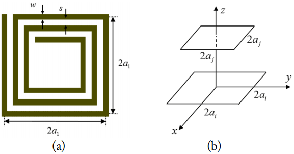
(a) A multi-turn spiral coil and (b) two single-turn filament coils.
where MS1,ij is mutual inductance between two coaxial single-turn coils, while the LS1,i is self-inductance of the coils. Additionally, the mutual inductance between an n-turn coil and m-turn spiral coils with distance d is obtained as:
For design simplicity, the coils are symmetrically designed. Fig. 5(a) shows the self-inductance and mutual inductance with a varying number of turns. Mutual inductance is also obtained when the air gap between two coils is set as 150 mm and the corresponding coupling coefficient is plotted in Fig. 5(b). The higher coupling coefficient is advantageous to efficiently transmit power because high magnetizing inductance can reduce the circulating current at the primary side, so a higher number of turns seems to be better. However, a longer wire decreases power efficiency due to the conductor resistive loss, resulting in a trade-off in coil design.
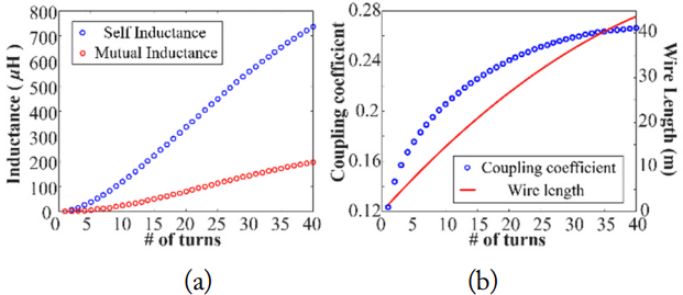
Calculated results of coil characteristics according to the number of turns: (a) self-inductance and mutual inductance and (b) coupling coefficient and wire length.
In this design, the number of turns selected is 15, since the coupling coefficient tends to be saturated at a higher number of turns. Self-inductance and mutual inductance calculated by analytical expressions (10) and (11) are summarized in Table 2. The analytical results were very similar to the 3-D simulation results using a commercial solver, Ansys Maxwell.
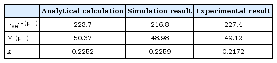
Self-inductance and mutual inductance of the design coils
The square-shaped spiral coils were manufactured using a Litz wire to reduce AC conductor resistance, and the self-impedance and transfer impedance of the coils were measured using the VNA. The inductance values extracted from the impedance measurements are predominantly constant at frequencies from 1 kHz to 200 kHz. The analytical, simulation, and experimental results show good agreement, as summarized in Table 2.
2. Design of Compensation Networks
A compensation network is essential for WPT systems, since the imaginary part of input impedance should be removed to achieve high-power transfer efficiency. Capacitors are usually employed for the compensation, and there are several topologies depending on how the capacitors are connected at the primary and secondary side coils, such as series-series (SS), series-parallel (SP), parallel-series (PS), and parallel-parallel (PP). Other high-order topologies, such as the LCC topology, are also applicable to practical WPT systems. The power transfer characteristics of different compensation topologies are well summarized in [9], and a proper topology can be selected to minimize the VA rating and achieve constant voltage or current.
A SS compensation network was employed for the WPT design here, which is the simplest topology for impedance compensation. Fig. 6 shows the circuit model of WPT coils and SS compensation networks with the arbitrary load ZL. For the symmetric primary and secondary coils, n1 = n2, the leakage inductance Lleak is calculated as (Lself − M), and the magnetizing inductance Lm is identical to the mutual inductance M [25]. Rloss implies the parasitic resistance from each coil and compensation network, including the equivalent series resistance (ESR) of the capacitors. The impedance parameters, Z11 and Z21, can be derived from the circuit model as:

Circuit model of the AC-AC stage of SS WPT topology with the load ZL, where n1 and n2 represent turn numbers of primary and secondary side coils.
where ZM = jωLM, Zleak = jωLleak, and Zc = 1/(jωC). Rloss is usually much smaller than the load impedance, and the summation of Rloss and ZL in (12) and (13) can be simply approximated to ZL.
There are two typical strategies for designing the SS compensation network. One is compensating for the self-inductance of a coil, which includes both leakage inductance and magnetizing inductance as shown in [26]. When the self-inductance compensation network is adopted at an operating frequency ωo,1, which implies (ZM + Zleak) + Zc = 0, ωo,1 can be written as:
Another compensation strategy is compensating for leakage inductance [8]. When the leakage inductance compensation network is adopted at the operating frequency ωo,2, which implies Zleak + Zc = 0, ωo,2 is written as:
Capacitors of 60 nF are chosen in this design so that the self-inductance compensation frequency ωo,1 and the leakage inductance compensation frequency ωo,2 are within the target frequency range for the manufactured coils. The self-inductance compensation frequency ωo,1 was obtained as 2π · 43.4 krad/s regardless of the distance between the coils. The leakage inductance compensation frequency ωo,2 was obtained as 2π·49.5 krad/s for a coil distance of 150 mm, but the frequency decreases with increased coil distance or any misalignments.
Substituting (12)–(15) into (1)–(6) and (9), the performance parameters can be consistently obtained using Z-parameters. The approximated expressions for the two compensation conditions are summarized in Table 3. It is assumed that Rloss is much smaller than the magnitudes of ZM and ZL. RL and XL represent the real and imaginary parts of the load impedance, respectively.

Performance parameters for two compensation conditions
As shown in Table 3, the self-inductance compensation can achieve the zero-phase angle (ZPA) condition at operating frequency ωo,1, if the imaginary part of the load impedance is negligible. Therefore, the output power is maximized at frequency ωo,1 regardless of the mutual inductance and load variation. However, one weakness of this compensation strategy is that input power, output power, and voltage gain can be significantly changed, depending on the distance between coils and load variation, which causes difficulty in the control circuit design of the power source or rectifier. Nevertheless, the leakage inductance compensation strategy can achieve the unity voltage gain at operating frequency ωo,2 regardless of the load variation. However, the operating frequency ωo,2 itself is changed by the distance and misalignment between two coils, since the leakage inductance depends on mutual inductance. Therefore, another control technique is needed to adjust the operating frequency. The expressions of the power transfer efficiency at both ωo,1 and ωo,2 are identical according to Table 3; yet, the efficiency variations around the frequencies ωo,1 and ωo,2 differ from each other due to the different assumptions for Rloss, which will be shown in the next section with the experimental results.
The operating frequency is initially set as ωo,1 in the WPT design herein. According to the analytical calculation results, the |V1| should be 30.71 to achieve 100 W output power at a 40 Ω load for the 150 mm air gap between the coils.
It should be noted that the proposed WPT performance extraction technique is a general design approach that can be used for arbitrary types of coupling coils and compensation networks. The SS compensation topology as well as the spiral coil shape have been chosen just as a design example.
V. Experimental Setup and Validations
Fig. 7(a) is the experimental setup for extracting the performance parameters of the manufactured WPT system in a frequency domain. A two-port VNA is used and ferrite beads are mounted on measurement cables to reduce common-mode (CM) noises. Cement resistors of 40, 60, 80, and 120 Ω are used as the equivalent AC resistance of the rectifier and load.
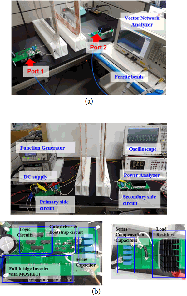
Experimental setup for (a) measurements using the VNA in a frequency domain and (b) power transfer measurements in a time domain.
The S-parameters of the AC stages in the WPT system have been measured with the load resistor connected, but the DC-AC power source disconnected, as depicted in Fig. 2. The measured S-parameters are then converted to Z-parameters, and Z11 and Z21 are substituted to (1)–(6) and (9). The impedance of the cement resistors, including large parasitic inductances, were separately characterized by the VNA measurements to achieve high accuracy, rather than directly utilizing the Eqs. (7) and (8). As mentioned in Section III, V1 corresponds to the fundamental frequency component of the DC-AC power source. When the power source is implemented with the full-bridge inverter and the first harmonic approximation is valid, the magnitude of V1 is equal to 4/π times that of Vdc. For the power source as the half-bridge inverter, it is 2/π times that of Vdc.
Fig. 7(b) is another experimental set-up for the actual power transfer measurements in a time domain to validate the WPT performance parameters extracted using the proposed method. A simple full-bridge inverter is implemented as the DC-AC power source in front of the primary compensation capacitors. Digital logic circuits are designed to generate the synchronous gate inputs to power MOSFETs. The gate driving inputs to the high-side MOSFETs are achieved by exploiting a bootstrap circuit with external fast transition diodes and bootstrap capacitors. The DC input voltage of 25 V is applied in front of a DC-link capacitor, and the maximum output power is expected to be 107.4 W for a 40 Ω load, according to the analytical result in Table 3. However, considering Rloss and switching loss in the inverter, the actual output power should be lower than the expected value. The power analyzer is used to simultaneously measure the input and output powers of the AC-AC stage.
Fig. 8 shows the measured voltage and current waveforms at different operating frequencies of 20 kHz and 40 kHz when the load resistance is 40 Ω and the distance between the two coils is 150 mm. At the 20 kHz operation, the high frequency harmonic distortion is significant, which is different from the operation at 40 kHz. The waveforms at the 20 kHz operation are also decomposed to each frequency component by Fourier series in Fig. 9. At the output stage, the third harmonic components are more dominant than the fundamental components. This indicates that the first harmonic approximation was not valid in this case, since the power transfer characteristics of the AC-AC stage are very poor at 20 kHz. The total powers and the powers of the first harmonic components at both input and output are plotted in Fig. 10. The first harmonic component is dominant at the frequencies above 25 kHz. Therefore, the effect of high frequency distortion is negligible near the target operating frequencies of 43.4 kHz and 49.5 kHz.
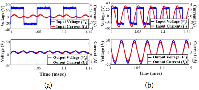
Voltages and currents measured by an oscilloscope at the operating frequency of (a) 20 kHz and (b) 40 kHz.

Fourier series of the measured waveforms for 20 kHz operation at (a) input and (b) output stages.

The total powers (Pin,total, Pout,total) and the powers of the first harmonic components (Pin,fund, Pout,fund) measured using a power analyzer at both the input and output stages.
In Fig. 11, the WPT performance parameters extracted by VNA measurements are compared with those from the measurements using the power analyzer in a time domain, when the distance between two coils is at 150 mm and the-load resistance changes. It should be noted that the measurements using the power analyzer are very sensitive to the parasitic impedances of the instrument and cables. Especially, only a few degrees of phase error at the input AC stage significantly affect the ratio of input real power and imaginary power in the WPT system. Therefore, the phase errors should be compensated to compare the measurement results using the power analyzer.
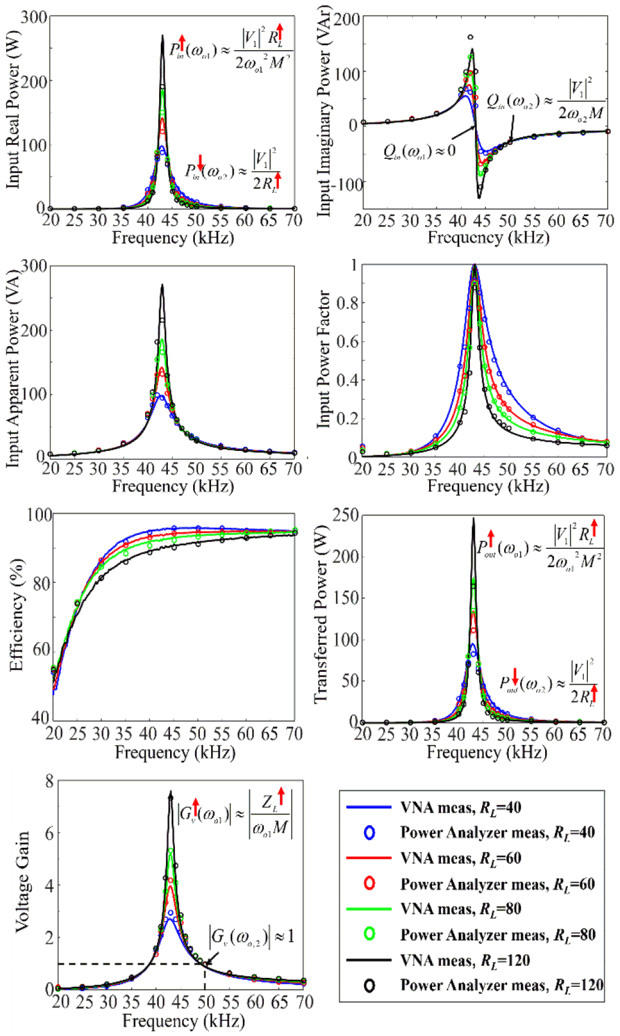
WPT performance parameters with various load resistances RL.
The zero imaginary power is achieved at 43.0 kHz, which is slightly smaller than the designed operating frequency ωo,1. Additionally, the unity gain is achieved at 50.0 kHz, which is also slightly different from the operating frequency for leakage inductance compensation ωo,2. The power efficiencies at 20 kHz, extracted using the two methods, have relatively large discrepancies due to the high frequency distortion. However, except for the input power factor and the power transfer efficiency at the 20 kHz operation, the discrepancies at other operating frequencies are acceptable by considering the tolerance of the components and the distance between two coils.
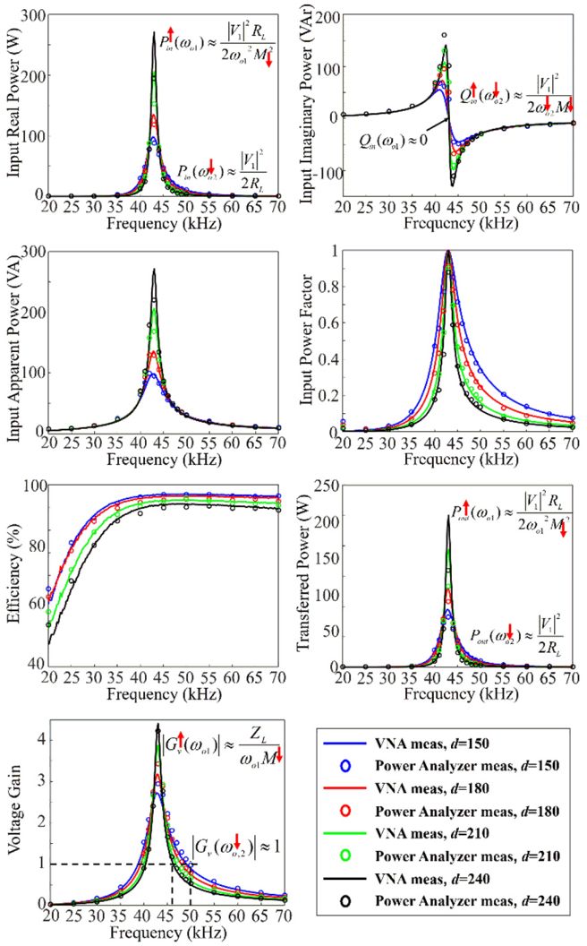
Fig. 12 shows the WPT performance parameters with different distances between two coils, which implies that the mutual inductance changes. The zero imaginary power is still achieved at 43 kHz regardless of the distance, because the self-inductance is independent of the mutual inductance. However, the gain is no longer constant at 50 kHz, since the leakage inductance depends on mutual inductance and the operating frequency ωo,2 decreases down to 46 kHz. The efficiencies in all the frequency ranges change by similar amounts, which is a different trend than in Fig. 11.
WPT performance parameters with various distances between two coils.
The efficiency and output power extracted by the VNA measurements are plotted again in Fig. 13 as a function of the load resistance and the distance between two coils, respectively. From these plots, the sensitivities of the efficiency and output power to the operating frequencies near 43 kHz and 50 kHz can be clearly compared. The transferred power is maximized but is very sensitive to the frequency near 43 kHz.

Efficiency and output power according to (a) the load resistance and (b) the distance between coils. The sensitivities to the operating frequencies near 43 kHz and 50 kHz are compared.
The output power at 43 kHz significantly increases as the load resistance and distance increase. It should be noted that the input impedance of the WPT system at the self-inductance compensation condition is expressed as the (ωo,1M)2/RL from equations (12)–(14). Thus, the input impedance at the self-inductance compensation frequency decreases when the load resistance increases or mutual inductance decreases; then, the input power increases if the input voltage is constant. However, when the power transfer efficiency through the WPT system does not decrease that much, the output transferred power also significantly increases.
If the input impedance of a WPT system is much lower than the source impedance of the power source, the power cannot be transferred through the WPT system. However, when the on-switching resistance in the inverter is very small to several hundred mΩ, the input and output power constantly increases at the self-inductance compensation frequency. Therefore, when the operating frequency for compensating the self-inductance is adopted, the operating frequency should be very accurately tuned, considering the tolerance of the device components and coils.
In summary, the operating frequency of 43 kHz can achieve a high output power and voltage gain, but the maximum value is drastically changed by any variations of frequency, load, and the distance between coils, as shown in Fig. 13. Meanwhile, an operating frequency around 50 kHz is relatively robust to frequency variations, but it is difficult to achieve a high output power and voltage gain, compared to the self-inductance compensation strategy. Therefore, instead of the two frequencies, operations at 42 kHz or 44 kHz could be a good option for a practical WPT system design. As shown in the Fig. 13, the transferred output power at 44 kHz is quite robust to variances of load and coil distance, while the output power is slightly smaller than at 43 kHz. The robustness can significantly reduce the burden in designing the control circuits of the power source and rectifiers for a practical high-power WPT system.
Considering the above practical design issues, the final operating frequency was selected as 44 kHz; thus, the DC input voltage should be increased to 31 V (|V1| = 39.47) to achieve the design target of 100 W output power at this operating frequency. The final performance parameters at the operating condition are summarized in Table 4. The final performance parameters from the time domain measurements are compared with those from the proposed method using VNA, when the load resistance is 40 Ω and the distance is 150 mm. The final measurement results in the time domain agree well with the estimation by the proposed method using frequency domain measurements as well as the initial design targets.
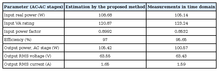
Final performance of the manufactured WPT system
VI. Conclusion
A new experimental optimization method for WPT systems based on frequency domain measurements was proposed. Various power transfer characteristics can be extracted by one passive measurement with consideration of the overall parasitic components in the compensation networks and coils. From the extracted performance parameters of the designed WPT system, the operational target for real WPT operations can be efficiently optimized in a frequency domain. The proposed method was demonstrated with an example for employing the WPT system design for an SS compensation network.
The proposed method provides the power transfer characteristics of only the AC-AC stages due to the limitations of frequency domain measurements. To consider the effects of power source and rectifier stages, additional circuit models of the inverter and rectifier losses can be further incorporated in the performance extraction step. With the proposed design flow, the performance of AC-AC stages and the optimal operational target of a WPT system can be accurately characterized and determined prior to the implementation of the power source and rectifier, which will facilitate an effective design process.
Acknowledgements
This work was supported by the Basic Science Research Program through the National Research Foundation of Korea (NRF) funded by the Ministry of Education (No. NRF-2016R1D1A1B03934382).
References
Biography

Sangyeong Jeong
received the B.S. degree in electrical engineering from the Ulsan National Institute of Science and Technology, Ulsan, Korea, in 2015, where he is currently pursuing the Ph.D. degree. His current research interests include electromagnetic compatibility (EMC) problems in the power system and the noise reduction techniques.

Mina Kim
received the B.S. degree in electrical engineering from the Ulsan National Institute of Science and Technology, Ulsan, Korea, in 2015. She is in combined M.S./Ph.D. course in UNIST. Her research interests include wireless power transfer (WPT), power electronics, and real-time simulation of power conversion systems.

Jee-Hoon Jung
received the B.S. degree in electronic and electrical engineering and the M.S. and Ph.D. degrees in electrical and computer engineering from the Department of Electronics and Electrical Engineering, Pohang University of Science and Technology (POS-TECH), Pohang, Korea, in 2000, 2002, and 2006, respectively. From 2006 to 2009, he was a Senior Research Engineer in the Digital Printing Division, Samsung Electronics Company Ltd., Suwon, Korea. From 2009 to 2010, he was a Postdoctoral Research Associate in the Department of Electrical and Computer Engineering, Texas A&M University at Qatar (TAMUQ), Doha, Qatar. From 2011 to 2012, he was a Senior Researcher in the Power Conversion and Control Research Center, HVDC Research Division, Korea Electrotechnology Research Institute (KERI), Changwon, Korea. From 2013 to 2016, he was an Assistant Professor in the School of Electrical and Computer Engineering (ECE), Ulsan National Institute of Science and Technology (UNIST), Ulsan, Korea, where he is currently an Associate Professor. His research interests include DC–DC converters, switched-mode power supplies, motor drives and diagnosis systems, digital control and signal processing algorithms, power conversion for renewable energy, and real-time and power hardware-in-the-loop simulations of renewable energy and power grids. Recently, he has been researching high-frequency power converters using wide bandgap devices, smart power transformers for smart grids, power control algorithms for DC microgrid, and wireless power transfer techniques for home appliance applications. Dr. Jung is a Senior Member of the IEEE Industrial Electronics Society, IEEE Power Electronics Society, IEEE Industry Applications Society, and IEEE Power and Energy Society. He has served as a Member of the Editorial Committee of the Korea Institute of Power Electronics.

Jingook Kim
received his B.S., M.S., and Ph.D. degrees in electrical engineering from Korea Advanced Institute of Science and Technology, Daejon, Korea, in 2000, 2002, and 2006, respectively. From 2006 to 2008, he was with DRAM design team in Memory Division of Samsung Electronics, Hwasung, Korea, as a senior engineer. From January 2009 to July 2011, he worked for the EMC Laboratory at the Missouri University of Science and Technology, Missouri, USA, as a postdoc fellow. In July 2011, he joined the Ulsan National Institute of Science and Technology (UNIST), Ulsan, Korea, where he is currently an associate professor. His current research interests include high-speed I/O circuits design, 3D-IC, EMC, ESD, RF interference.