Study on Timing Characteristics of High-Voltage Pulse Generation with Different Charging Voltages
Article information
Abstract
The time synchronization of each sub-unit of a pulsed generator is important to generate an output high-power radio frequency (RF) signal. To obtain the time synchronization between an input RF signal fed by an external source and an electron beam produced by an electric pulse generator, the influence of different charging voltages on a delay and a rise time of the output pulse waveform in the electric pulse generator should be carefully considered. This paper aims to study the timing characteristics of the delay and the rise time as a function of different charging voltages with a peak value of less than −35 kV in the high-voltage pulse generator, including a trigger generator (TG) and a pulse-forming line (PFL). The simulation has been carried out to estimate characteristics in the time domain, in addition to their output high-voltage amplitude. Experimental results compared with those obtained by simulation indicate that the delay of the output pulses of the TG and PFL, which are made by controlling the external triggering signal with respect to different charging voltages, is getting longer as the charging voltage is increasing, and their rise times are inversely proportional to the amplitude of the charging voltage.
I. Introduction
Pulsed power systems with a high-voltage pulse have been developed to produce a high-power electromagnetic pulse using a switch that can handle the high-voltage capacity and that can be triggered by an external triggering pulse to synchronize with the system. For example, the high-power electromagnetic pulse can be produced by sending the external triggering signal into a spark gap switch installed before a broad impulse antenna, after charging the high-voltage spark gap switch regulated by changing the insulating gas pressure and the gap distance between the two main electrodes of the spark gap switch [1]. Another way to produce a high-power electromagnetic pulse is using a vacuum amplifier that emits an intense electron beam from the cathode that interacts with a microwave provided by an external driver in an input cavity. For an efficient interaction between an intense electron beam and the input cavity, the voltage for the cold cathode emission needs to reach above a threshold level of 140 kV [2]. Therefore, key technical points to get the high-power electromagnetic pulse are essentially dependent on whether and how much electrical pulse energy with more than a couple hundred kilovolts is gained. This is because it is related directly to an electron beam acting as a key factor when it interacts with the external radio frequency (RF) input signal at the input part in the vacuum tubes [3]. There are largely two steps to generate an electrical pulse with more than a couple hundred kilovolts in a pulsed generator. First, direct current (DC) volts will be charged up to several tens of kilovolts. Then, high-voltage stacking will be conducted using a trigger generator (TG) to produce a high-voltage electrical pulse by charging many capacitors in parallel. If there is no voltage loss in this circuit, the target amplitude of the voltage is equal to the result of multiplying the number of stacking capacitors by the amplitude of the voltage of the single capacitor. To get the optimum value of the target voltage amplitude, therefore, the characteristic of a high-voltage switch connecting one stage to another in the capacitor bank plays a key role [4]. Moreover, it can influence the general performance of a pulsed generator. This is why it is so important to research the characteristics of the high-voltage switch.
Another thing that must be considered to generate a good waveform at the output of a pulsed generator after achieving an acceptable high-voltage level at the voltage stacking structure is a pulse-forming line (PFL) as a sub-system of a pulsed generator. It can largely be categorized into a pulse-forming network [5–8] and a PFL [9–12]. The pulse-forming network can be applicable to creating a long pulse duration, but it has the disadvantage of having many parasitic components and low flexibility to the impedance of the load comparatively. However, the PFL can be useful for creating a short pulse duration, and it has good compatibility with the load impedance match compared to the pulse-forming network.
Fig. 1 shows the general timing diagram for generating a high-power RF signal in a pulsed power system including a vacuum tube. It indicates how the vacuum tube is operated. First, a driver can be ready by receiving the trigger by signaling a pulse modulator and the enable time signal sequentially, which results in its RF pulse. Second, a pulsed magnet for producing a sufficient magnetic field to guide the electron beam in the vacuum tube given by a pulsed generator during the enable time can be operated by the external trigger on the signal. Third, a pulsed generator can produce an electron beam when the triggering signal is given. Lastly, the RF pulse from the output port of the vacuum tube can be attained within the duration of the electron beam.
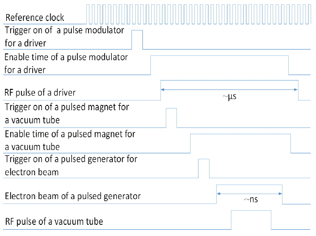
General timing diagram for capturing an RF signal in a vacuum tube.
As explained above, an analysis in the time domain is important to determine whether all of the parameters related to the high-power RF generation through a vacuum tube are synchronized with each other. Particularly, time synchronization in a pulse generator should be analyzed because it has a time length in nanoseconds, and the characteristics of the output electric short pulse of a pulsed generator can have a significant impact on the generation of an electron beam as a source of the vacuum tube.
If the output RF pulse level of the pulsed generator is tuned by the variation in the electron beam intensity with the fixed input RF pulse level driven by a driver instead of the variation in the driver’s RF pulse power level, the interaction timing in an input cavity of a vacuum tube between the input RF pulse and the electron beam driven by the electric pulse generated by high-voltage pulse generator can largely affect the output RF pulse power level of the pulsed generator.
However, conventional studies have relatively rare data on the time-varying characteristics of a high-voltage pulse with the amplitude of more than −500 kV. Therefore, a time analysis of the generation of an electric high-voltage pulse driving the electron beam of a pulsed generator is the focus of this paper. In particular, pulse characteristics over time produced by a TG and a PFL are researched in detail, because the output power level and efficiency of a vacuum tube depend largely on the time synchronization of the electron beam driven by the electric high-voltage pulse with the input RF signal in the vacuum tube.
II. Design
1. Design of the Capacitor-Charging Power Supply
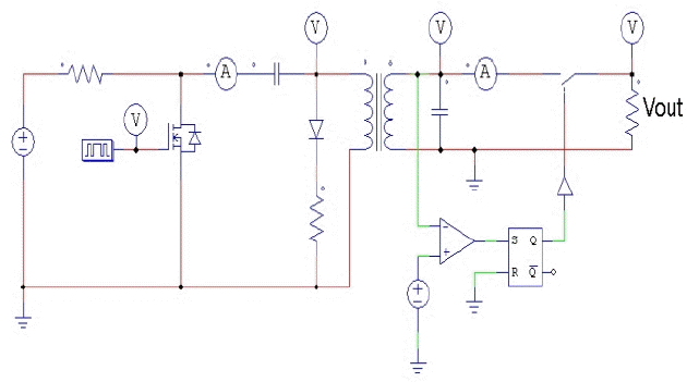
A capacitor-charging power supply (CCPS) having an output voltage of more than 100 kV is designed to charge capacitors in the high-voltage stacking circuit (HVSC) and is simulated with PSIM [13].
It is designed to work from 60 Hz with three-phase and 380 volts in alternating current (VAC). Its AC input is full-wave rectified through the rectifier. After that, a filtered voltage at the capacitor attained on the secondary of the first transformer is delivered to the second transformer, called the main transformer, through the inverter module to get the target-filtered voltage by the full-bridged rectifier on the secondary of the second transformer, as shown in Fig. 2. It has a rise time of less than 2 ms to reach the desired output voltage of 100 kV, as shown in Fig. 3.
Circuit diagram of the CCPS.
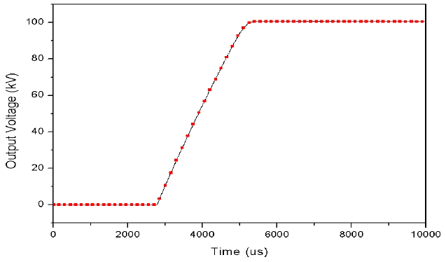
The simulated maximum output voltage of the CCPS.
Fig. 4 indicates the primary current with the maximum value of 572 A of the main transformer having a turn ratio of 196 to 1, and Fig. 5 shows the secondary current with a maximum value of 2.91 A of that in the CCPS.

The simulated primary current of the main transformer in the CCPS.
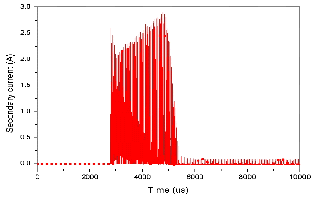
The simulated secondary current of the main transformer in the CCPS.
2. Design of the TG
Fig. 6 indicates the circuit diagram of the TG simulated by PSIM. Its applied input voltage is set to 300 VDC as a bus voltage by taking into account the full-wave rectification and power loss with the input voltage, frequency, and phase at 220 VAC, 60 Hz, and single, respectively. Detailed values in millimeters of the design parameter of the spark gap of the TG are shown in Fig. 7.
Circuit diagram of the TG.
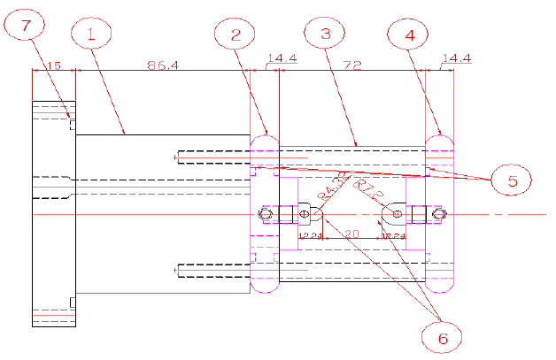
Designed spark gap of the TG.
Fig. 8 indicates the primary current and voltage at the transformer having the turn ratio of 2 to 400. When the critical level of the output voltage in the circuit with the load resistance of 6 MΩ is set to −60 kV, the characteristic of the rise time is shown in Fig. 9.
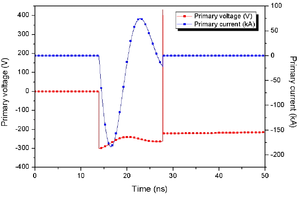
The simulated primary current and voltage of the transformer in the TG.
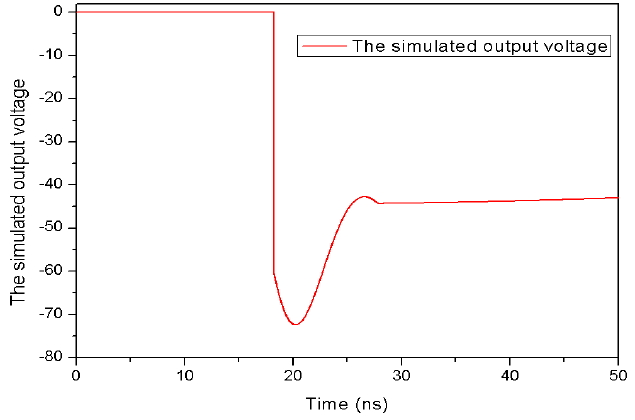
The simulated output voltage of the TG.
The spark gap of the TG is set to remain at a high resistance to the circuit initially so that capacitor installed in front of the spark gap is allowed to charge until the breakdown voltage of the spark gap is reached.
The number in Table 1 describing parameters of the design of the TG indicates the index circular number, as shown in Fig. 7.

3. Design of the PFL
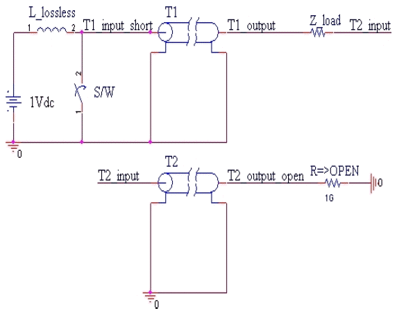
To produce a pulse duration of more than 100 ns and to keep the same amplitude between the charging voltage and the load voltage, a PFL, called the Blumlein PFL [14], with two transmission lines, as shown in Fig. 10, is designed if it is more sensitive to parasitic inductance.
Circuit diagram of a PFL with two transmission lines.
The load impedance (ZL) of the PFL, comprised of two lossless transmission lines, is shown in Eq. (1).
where Zo,PFL is the characteristic impedance of the transmission line, ɛr is the relative permittivity of deionized water as a dielectric, μr is the relative permeability of deionized water as a dielectric, Ro is the radius of the PFL’s outer conductor, and Ri is the radius of the PFL’s inner conductor.
The maximum pulse duration on the condition of a full width at half maximum (FWHM) can be defined, as shown in Eq. (2)
where l is the length of each transmission line and c is the speed of light in a vacuum.
If a pulsed generator with this PFL is one of the sub-systems in a transceiver system, the pulse duration, which is dependent on the PFL, plays a crucial role as a system parameter in terms of whether its performance is effective against any threat, because the pulse duration is related to the transit time in a vacuum tube with a cavity.
Fig. 10 shows a conceptual configuration of the PFL with two lossless transmission lines. When the voltage Vinput = 1 VDC is applied to the input terminal and then the switch is closed, an input voltage signal will flow toward the load Z_load, where it will be reflected with a reflection coefficient of 0.5.
The part where inner and middle conductors are connected has a reflection coefficient of −1, and the reflection coefficient at the end of the transmission line comprised of middle and outer conductors is 1.
If the switch is closed at the time of 60 ns after charging and the transmit time of two transmission lines of T1 and T2 is 60 ns each, the lossless PFL can produce a pulse duration of 120 ns. Figs. 11 and 12 describe the voltage formation at both end terminals of T1 and T2 over time.

Voltage distribution formed on the left and right terminals of T1 over time.

Voltage distribution formed on the left and right terminals of T2 over time.
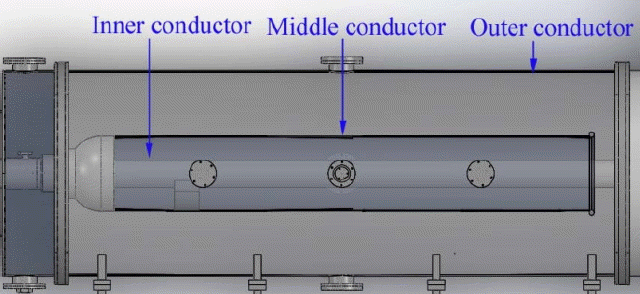
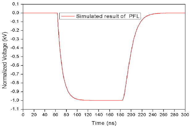
The structural diagram of the PFL is shown in Fig. 13. A simulated pulse duration of 120 ns on the condition of a FWHM with a voltage of −1 kV is shown in Fig. 14.
Schematic of the PFL structure.
The simulated pulse waveform of the PFL.
To withstand the applied high voltage of down to −500 kV without the electric breakdown and to lessen the physical length of the PFL, the deionized water was used as a dielectric of the PFL. Table 2 indicates the radius and physical length of each connector of the PFL. Two designed transmission conductors have been submerged in deionized water to calculate the characteristic impedance of the PFL as a coaxial cable structure.
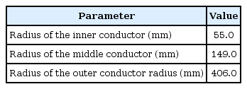
Design parameters of the PFL
All of conductors making up the PFL have been designed to be immersed in the deionized water with a relative permittivity of 78.3 to calculate the characteristic impedance of the PFL as that of a coaxial structure [15].
III. Experiment Results
The fabricated spark gap of the TG is shown in Fig. 15. The measured rise time of the TG is shown in Fig. 16, and it is 7 ns longer than its simulated rise time at the point where it reaches an output voltage of −60 kV.

Fabricated spark gap of the TG.
Measured rise time of the output voltage of the TG.
This slight rise time difference between the measured and simulated results can be explained by the inference, which is caused by the difference in capacitance between the output port cable of the TG and the high-voltage probe of the measurement instrument. In addition, the time difference in reaching the peak output voltage would result from the effect of the capacitance and inductance in the circuit.
The experiment was carried out 10 times, as shown in Fig. 17, with a time step of one minute and two different N2O2 gas pressure levels of 0.3 MPa and 0.4 MPa. A bare cable composed of metal composite wire having a combination of tungsten combined with copper at a percentage of 30% to 70%, respectively, has been applied to achieve an output voltage of down to −100 kV of the TG.
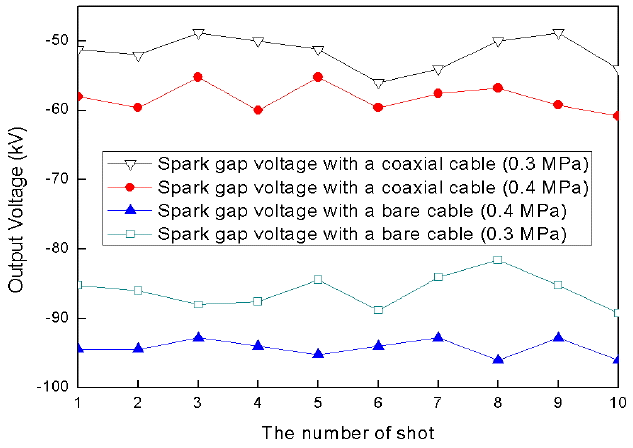
Breakdown voltage with different cable types and pressure levels.
The breakdown voltage is higher when a bare copper cable is applied compared to a coaxial cable and a higher pressure is applied. For each shot, it can be seen that it is constant typically if the experimental condition is the same.
The time delay between the applied charging voltage and the breakdown voltage is approximately linearly proportional to the amplitude of the breakdown voltage, as shown in Fig. 18.
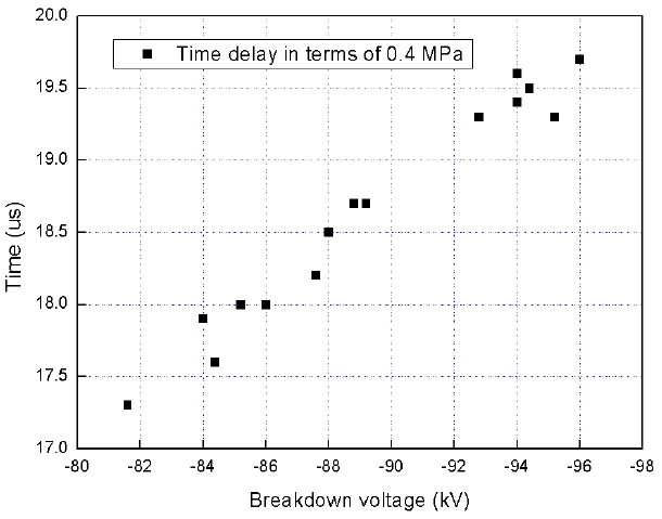
Time delay in terms of 0.4 MPa.
We have conducted an experiment by applying the output signal of the TG to the HVSC comprised of eight high-voltage spark gap switches to analyze how the rise time will change when the applied voltage increases. The spark gap switch of Model 40265 made by L3 is used as an active load instead of a resistive load in this experiment.
As the charging voltage increases, the rise time of the output voltage signal gets shorter generally, as shown in Fig. 19. Special care with the gas pressure across the electrodes within the spark gap switch must be taken to ensure the spark gap is closed without any effect of variations in pressure across two electrodes.
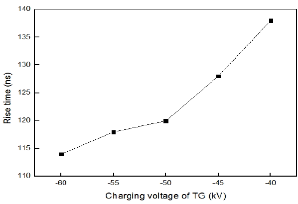
Fitting curve of the rise time with respect to different charging voltages.
The measurement setup for analyzing the time delay of a pulsed electric generator is composed of the CCPS, the TG, the HVSC, and the PFL.
A fabricated PFL is shown in Fig. 20. Ground impedance was set to be less than 10 Ω to suppress the floating noises in which the high-frequency components are related to the very fast rising part of the transient, while the low-frequency components are related to the long tail part. High-voltage waveforms are well captured simultaneously over time from the TG, the HVSC, and the PFL.
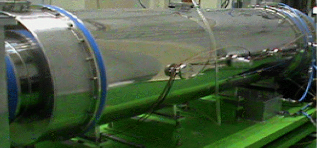
Fabricated PFL.
Typical waveforms over time are formed, as shown in Fig. 21. The time sequence is largely divided into three stages. First, the output voltage of the TG is produced, and then this signal is applied to the HVSC to charge the high-voltage target to drive the PFL. Finally, charging and discharging occur in the PFL to generate a high-voltage short pulse with the designed pulse duration.
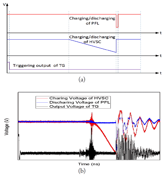
Typical waveforms with respect to time. (a) Individual charging and discharging sequence. (b) The triggering output of the TG, the charging of the HVSC, and the discharging of the PFL.
Once the control signal being actively high is optically delivered to the TG, the output pulse signal of the TG is generated after reaching the target charging voltage level of the TG in around 2–7 μs. Then, the HVSC is charged up to the breakdown level for around 3 μs, as shown in Fig. 22.
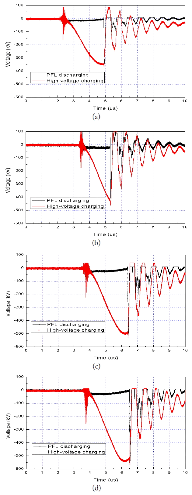
Time characteristic of measured output waveforms with respect to the change in charging voltage: (a) −35 kV, (b) −45 kV, (c) −50 kV, and (d) −55 kV.
The PFL begins charging and discharging for a time designed by twice the electrical length of the transmission. Reflected pulse signals emerge after the main pulse is generated due to a stray impedance condition. For example, if the HVSC is charged down to −45 kV, the amplitude of the output pulse signal of the PFL reaches around −450 kV, as shown in Fig. 22.
The reason why the charging time is longer when the charging voltage is higher is discussed. As the target charging voltages of the spark gap switch installed in the TG are −35, −45, −50, and −55 kV, as shown in Fig. 22, the output signals of the TG appear around 2.5, 3.5, 3.7, and 3.8 μs, respectively. Each delay reflects how long it takes to get the target breakdown voltage amplitude, as the wanted breakdown level is higher. As soon as the output signal of the TG is generated, the high-voltage process in the HVSC is started. The process of charging the HVSC is completed from 5.0 to 6.5 μs, depending on the amplitude of the output voltage of the HVSC. A high-voltage pulse is produced after completion of charging the HVSC for the period during which the pulse duration is linearly proportional to the electrical length of the PFL. This means the internal triggers in the pulsed generator must be matched with the delay and the rise time of the electric high-voltage pulse generated by the high-voltage pulse generator in a time domain when the amplitude of the charging voltage in the pulse generator is lowered or raised to get the changeable output RF pulse level of the pulsed power generator with the fixed input RF pulse level driven by a driver instead of the variation in the input RF pulse power level driven by it.
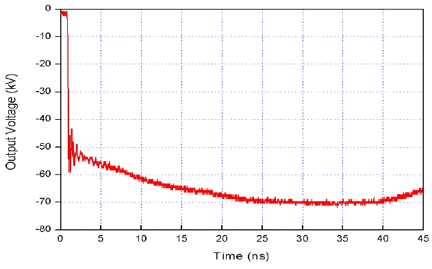
The agreement on the simulated and measured amplitudes of the output voltage with down to −500 kV at the peak point is shown in Fig. 23, and the measured rising trace is followed by the simulated rising trace. Furthermore, the measured pulse duration is around 120 ns at the FWHF compared to the simulated pulse duration. However, the measured voltage pulse contains a slight ripple due to a stray capacitance.
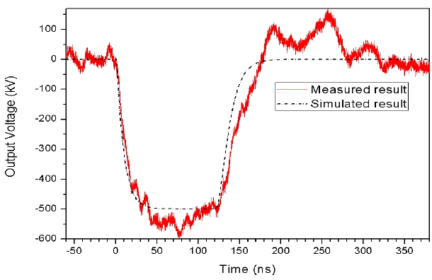
The result of the output pulse waveform of PFL.
IV. Conclusions
In this paper, a time analysis with the output electric pulses of the TG and the PFL composing the pulsed generator was performed.
It was found that the delay in the output electric pulses of the TG and the PFL, which are made by controlling the external triggering signal through different charging voltages, is proportional to the amplitude of the charging voltage, and their rise time gets shorter as the charging voltage increases.
The simulation has been carried out using PSIM and PS-PICE codes to estimate characteristics over time, such as the high-voltage amplitude, the rise time, and the pulse duration of its output pulse waveform. Data achieved through the simulation have been used for its fabrication. It has been tested to verify that the high-voltage pulse waveform has been generated without breakdown, and its delay and rise time attained repeatedly have a consistent relation with the change in the amplitude of the charging voltage. Results from simulations have been compared with those obtained experimentally.
The time analysis presented in this paper can be helpful for designing a vacuum tube to produce a relativistic output RF signal in terms of the time synchronization of an input RF signal with an intense electron beam.
References
Biography

Ki Wook Lee received B.S. and M.S. degrees in electronic engineering from Kwangwoon University, Seoul, Korea, in 2000 and 2002, respectively. He is currently working toward the Ph.D. degree in the department of electrical and electronic engineering at the University of Yonsei, Seoul, Korea. He was a research engineer from 2001 to 2004 at LG Innotek. Since 2005, he has been with LIG Nex1 at the R&D laboratory of Electronic Warfare, especially Electronic Attack. His current research interests include high-power vacuum amplifiers, high-voltage pulsed generators, and high-power microwaves.

Wangyong Lee received a B.S. degree in electronic engineering from Kyungpook Sanup University, Gyeongsan, Korea, in 1995 and an M.S. degree in information and electronic engineering from Ajou University, Suwon, Korea, in 2008. Since 1995, he has been working as a system engineer in Electronic Warfare division at LIG Nex1 Co. Ltd. His current interests include EW high-power array transmitters and EW systems.

Jung Ho Kim received B.S., M.S., and Ph.D. degrees in physics from Pohang University of Science and Technology, Pohang, Korea, in 2002, 2006, and 2010, respectively. Since 2010, he has been working as a researcher at LIG Nex1 Co. Ltd. His current interests include high-power microwaves and THz systems.

Woo-Joong Kim received a B.S. degree in electronics and information from Kyung Hee University, Suwon, Korea, in 2011, and he is currently working toward the M.S. and Ph.D. degrees in electrical and electronic engineering from Yonsei University, Seoul, Korea. Since 2011, he has been working as a Research Assistant at Yonsei University involved in the project of channel modeling. His research interests include radio propagation, underwater acoustic channels, high-power microwaves, and high-power antennas.
Seungsub Oh received a B.S. degree in electronic engineering from Chosun University, Gwangju, Korea, in 1989. Since 1989, he has been working as a research engineer at LIG Nex1 Co. Ltd. His current interests include high-power microwaves and EW systems.

Young Joong Yoon received B.S. and M.S. degrees in electronic engineering from Yonsei University, Seoul, Korea, in 1981 and 1986, respectively, and a Ph.D. degree in electrical engineering from the Georgia Institute of Technology, Atlanta, USA, in 1991. From 1992 to 1993, he was a Senior Researcher with the Electronics and Telecommunications Research Institute (ETRI), Daejeon, Korea. In 1993, he joined the faculty of Yonsei University, where he is currently a Professor with the Department of Electrical and Electronics Engineering. In 2012, he was president of the Korean Institute of Electromagnetic Engineering & Science (KIEES). His research interests include high-power antennas, high-power microwaves, and radio propagation.