Sensitivity Enhancement of a Vertical-Type CMOS Hall Device for a Magnetic Sensor
Article information
Abstract
This study presents a vertical-type CMOS Hall device with improved sensitivity to detect a 3D magnetic field in various types of sensors or communication devices. To improve sensitivity, trenches are implanted next to the current input terminal, so that the Hall current becomes maximum. The effect of the dimension and location of trenches on sensitivity is simulated in the COMSOL simulator. A vertical-type Hall device with a width of 16 μm and a height of 2 μm is optimized for maximum sensitivity. The simulation result shows that it has a 23% better result than a conventional vertical-type CMOS Hall device without a trench.
I. Introduction
Magnetic sensors are commonly used in various applications, such as the contactless measurement of current [1], magnetic resonance imaging [2], or biosensors [3], which require the accurate measurement of the magnetic field. A Hall sensor is a type of magnetic sensor that is widely used because of its capability to integrate into the CMOS process. The typical architecture of a Hall sensor consists of a Hall device, a chopper-stabilized amplifier, and a modulator, among others [4–6]. Although a Hall sensor includes circuits that can reduce the DC offset and amplify the signal for a high signal-to-noise ratio, a Hall device is still the most important because it is the front-end block that turns the external magnetic field into an electrical signal. Two types of Hall devices are implemented in the CMOS process: a horizontal-type Hall device (HHD) and a vertical-type Hall device (VHD). An HHD is designed to sense an external magnetic field, which is perpendicular to the wafer surface. However, in some applications such as magnetic communication, the measurement of a magnetic field in 2D or 3D is necessary for better accuracy in a space, which mandates the sensing of a magnetic field that is parallel to the wafer surface. A VHD depends on the vertical current flow in N-well and can be used in combination with HHDs for the 2D or 3D sensing of a magnetic field. However, VHDs suffer from low sensitivity and a large offset when compared with HHDs [7]. Sensitivity is critical for a CMOS VHD because a magnetic input signal is usually small, and the DC offset and 1/f noise are not negligible at a low-frequency region [8]. One of the most popular methods to reduce the offset of a VHD is a four-folded and three-contact (4F-3C) structure, but its sensitivity is still limited [9, 10]. This structure consists of four basic VHDs, and the sensitivity of each VHD contributes to the overall sensitivity. Therefore, the sensitivity of a single VHD needs to be improved regardless of the offset reduction feature. We intend to introduce a technique to achieve high sensitivity. The current-mode operation of a VHD is advantageous because its temperature dependency is low, and the ohmic voltage drop in the interconnection barely affects the performance [11]. It also provides better sensitivity [12]. For these reasons, current-mode VHDs are used throughout this work.
This paper is organized as follows. Section II analyzes a conventional VHD and explains its operation. A method to improve sensitivity is then proposed. Section III shows the optimization process of a VHD and some of the simulation results obtain from the COMSOL simulator.
II. Vertical-Type Hall Device
1. Operation and Analysis of the Current-Mode VHD
In a VHD, the current does not flow straight as in an HHD. Fig. 1 shows the current-mode VHD model implemented in the CMOS process with a bias current of Ibias. The bias current goes into the VHD through the input terminal C2 in the middle, and it propagates as illustrated in Fig. 2. As the two current output terminals are on the sides of the input terminal, most of the current flows along the wafer surface, and only a small portion of the current flows near the bottom, making a long detour due to Ohm’s law. Therefore, the horizontal current density is higher than the vertical current density near the input terminal. The direction of the current density significantly affects the Hall output current and thus sensitivity.

Current-mode VHD implemented by N-well in the CMOS process.
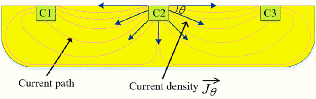
Current density distribution and current path in the 2D VHD model.
The current density in Fig. 2 is expressed by Eq. (1), the charge velocity by Eq. (2), and Lorentz force by Eq. (3).
where μn is the Hall mobility, n is the carrier concentration, and
By combining the expressions in Eqs. (2) and (4), we can obtain Eq. (5), which shows the relationship between the magnetic force and the current density.
where RH is the Hall coefficient and is equal to
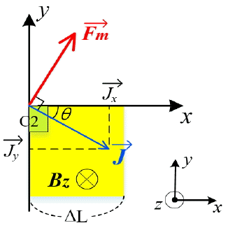
Direction of magnetic force vs. current density.
The total magnetic force on the current toward C3 can be derived from J⃗. It is expressed by Eq. (7) with the assumption that the magnetic field is constant and exists only in the z-direction.
In steady state, charges are accumulated on one side of the Hall device because of
As mentioned above, sensitivity is determined around the terminal C2 within the distance of ΔL. The Hall voltage is an integral of the Hall electric field as expressed in Eq. (9).
As dL⃗ is in the x-direction, Eq. (9) can be simplified as Eq. (10).
As the VHD operates in the current mode, Eq. (10) needs to be converted to a current equation. By applying Ohm’s law and using Rin, which is defined in Eq. (11) [12], the Hall current is expressed by Eq. (12):
where W is the width, L is the length, and t is the thickness of the VHD shown in Fig. 1. Eq. (12) shows that the current density in the x-direction does not contribute to the Hall current. The current along the y-axis is expressed by Eq. (13). We obtain Eq. (14) by substituting Eq. (13) into Eq. (12).
The sensitivity of a VHD in the current mode is expressed in Eq. (15). From Eqs. (14) and (15), we obtain Eq. (16).
In Eq. (16), μn and t are usually determined by the process. Therefore, Iy/IBias needs to be increased for high sensitivity. The increase in Iy/IBias indicates that more current needs to flow through the longest path in a VHD. However, the resistance increases as the current path becomes longer. The current path in a VHD can be modeled as the parallel resistors shown in Fig. 4. To increase Iy/IBias, more current needs to flow through the high-resistance path in Fig. 4. This action violates Ohm’s law, but the implantation of a trench in N-well causes change in the resistance distribution and can lead the current flow as intended.
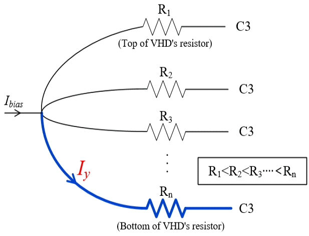
Resistive model of the current path from C2 to C3.
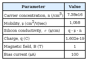
2. Sensitivity Enhancement by Trench Implantation
According to the analysis on a conventional VHD in Section II-1, the sensitivity of a VHD will increase if more current flows perpendicular to the surface around the terminal C2. For this change of current flow, a current-blocking trench can be implanted next to C2, as shown in Fig. 5. The trench does not need to be dielectric, but it can be formed simply by p-doping on N-well. The trench affects the resistive distribution in Fig. 4, and the resistance of the longest path becomes the smallest. It guides the bias current to flow vertically and helps to increase the sensitivity of a VHD. However, as the trench becomes deeper or wider, the input resistance of a VHD, Rin in Eq. (12), increases significantly, and sensitivity starts to decrease. Therefore, there exists an optimized dimension of a trench and its location for maximum sensitivity.
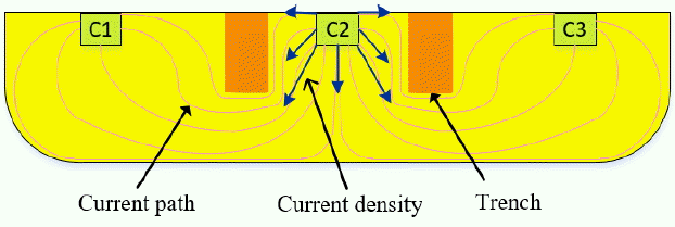
Current density distribution and current path in the 2D trench implanted in a VHD model.
The implantation of trenches on N-well is advantageous to sensitivity, but it may contribute to the DC offset because of the variation in the CMOS process. However, this offset can be easily suppressed by the 4F-3C structure using the current spinning [9, 10] and is not significant in most cases.
III. Simulation Results
1. Conventional VHD
A Hall device is usually modelled and simulated in 2D. First, a conventional VHD in the current mode is designed and simulated in the COMSOL simulator. The VHD is sized to have a width of 16 μm and a height of 2 μm. The width of the input terminal is 1 μm, and the output terminals have a width of 0.5 μm as half of the input current flows in each output terminal. The height of all terminals is 0.1 μm. In this work, a fixed voltage is used at the input terminal instead of a fixed current to generate bias current throughout the simulations. In the CMOS process, the use of a fixed current may cause overvoltage if the resistance of a VHD increases. Fig. 6 shows the simulated electric potential and the current density distribution in a VHD when the input terminal is biased by 100 μA and the magnetic field is 1 T. The sensitivity of the reference VHD is 0.0095 (T−1). Table 1 shows the model parameters used for the COMSOL simulation.
Current density distribution of a conventional current-mode VHD. Arrows represent the current density, and color means the current density in the y-axis.
Hall device model parameters
2. Proposed VHD with Trench Implantation
Fig. 7 shows the simulation model of a VHD with implanted trenches. Both the dimension of the trenches and their location affect the current density distribution, thus contributing to the sensitivity of a VHD. To evaluate the effect of a trench on sensitivity, we choose three variables, namely, height, width, and distance, between the input terminal and the trench. We can optimize the sensitivity of a VHD by analyzing the effect of each variable.
Trench implantation in the VHD.
2.1 Distance
We vary the distance between the input terminal and the trench from 0.1 μm to 1.3 μm by a 0.1 μm step, and the height and the width are fixed at 0.5 μm. Fig. 8 shows the simulated sensitivity versus distance, with sensitivity being inversely proportional to distance. The reason for this is that the bias input current flows in parallel with the surface, and the Hall current decreases as the distance increases. Therefore, the trench needs to be as close to the input terminal as possible.

Simulated sensitivity of the VHD vs. trench distance.
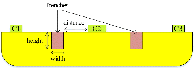
2.2 Width
Trench width can also affect the sensitivity of a VHD because it changes the current density distribution. The width is varied from 0.1 μm to 1.7 μm by a 0.2 μm step, and the height changes from 0.5 μm to 0.9 μm by a 0.1 μm step. The distance is fixed at the minimum of 0.1 μm to maximize sensitivity. Fig. 9 shows the simulated sensitivity versus the trench width. Sensitivity decreases as the width increases for all values of height. This inverse proportion comes from the resistance change of the VHD. If the trench width increases, the resistance between the terminals (Rin) becomes large. The increased Rin reduces the ΔIHall as indicated in Eq. (12). Therefore, sensitivity is inversely proportional to the trench width.
Simulated sensitivity of the VHD vs. trench width.
2.3 Height
The trench height is directly related to the direction of the current density around the input terminal. The trench height is varied from 0.1 μm to 1.2 μm by a 0.1 μm step for a width of 0.1 μm and 0.2 μm, and the distance is fixed at 0.1 μm. As shown in Fig. 10, sensitivity becomes maximum at a certain value of height. When the height is small, sensitivity increases as the height increases. The reason for this is that more current will flow in the vertical direction if the trench is higher. However, the sensitivity of a VHD begins to decrease when the height is over 0.8 μm. Although the directivity of the current density is improved, the resistance between the terminals increases, thus reducing the sensitivity. As the height of N-well is 2 μm, the sensitivity has an optimal value when the trench is sized to be approximately 40% of the height of N-well.
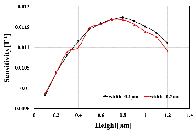
Simulated sensitivity of VHD vs. trench height.
3. VHD Simulation with an Optimized Trench
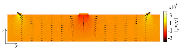
From the result above, we optimize a VHD with implanted trenches for maximum sensitivity. The trench is sized to have a width of 0.1 μm and a height of 0.8 μm. The distance between the trench and the input terminal is 0.1 μm. Fig. 11 illustrates the simulated current density distribution. As expected, the current density is guided in the vertical direction around the input terminal unlike the conventional one, as shown in Fig. 12. Consequently, ΔIHall increases (Fig. 13), and sensitivity is calculated as 0.011734 (T−1), which is 23% better than that of the conventional one.

Current density of the proposed VHD with optimized sensitivity. Arrows represent the current density, and color means the current density in the y-axis.
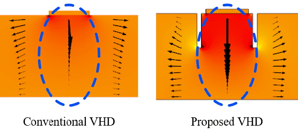
Current direction comparison of the conventional VHD and the proposed VHD near the input terminal. Arrows represent the current density, and color means the current density in the y-axis.
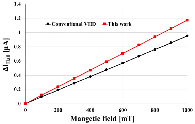
Hall current of the conventional VHD vs. the proposed VHD.
IV. Conclusion
This study analyzes a conventional VHD and the reason for its low sensitivity. Then, a new method of trench implantation is proposed to increase the sensitivity. The implanted trench next to the input terminal changes the direction of the current flow vertically. Therefore, the resultant Hall current is generated maximally. Three types of dimensional factors of the trench affect sensitivity. In the simulation results, the trench width and the distance between the trench and the input terminal are inversely proportional to sensitivity. Conversely, the trench height produces a curve, and the sensitivity is optimized by a certain height. When the three factors of the trenches are optimized simultaneously, the result shows 23% higher sensitivity than that of the conventional one without trenches. The trench can be implanted on N-well without any post-processing of the wafer. Therefore, we can achieve the higher sensitivity of a VHD, which is useful in a 4F-3C structure using the current spinning.
Acknowledgments
This work was supported by the Basic Science Research Program through the National Research Foundation of Korea funded by the Ministry of Science, ICT, & Future Planning (No. NRF-2015R1C1A1A01054385) and by the Institute for Information & Communications Technology Promotion grant funded by the Korean government (MSIP) (No. 20160001360022003, Development of a Hall Semiconductor for a Smart Car and a Device).
References
Biography

Sein Oh was born in Seoul, Korea in 1991. He is currently an undergraduate student in electronic engineering from Kookmin University, Seoul, Korea. His research interests are Hall Sensor, mixed signal, data conversion, and circuit design.

Hyungil Chae was born in Seoul, Korea, in 1981. He received his B.S. degree in electrical engineering from Seoul National University, Seoul, Korea, in 2004, and his M.S. and Ph.D. degrees in electrical engineering from the University of Michigan, Ann Arbor, MI, USA, in 2009 and 2013, respectively. From 2013 to 2015, he was a senior engineer at Qualcomm Atheros, San Jose, CA, USA. He joined Kookmin University, Seoul, South Korea, in 2015, and is currently an assistant professor. His research interests include mixed signal and RF circuit design. Dr. Chae is the recipient of a KFAS Fellowship.

Byung-Jun Jang received his B.S., M.S., and Ph.D. degrees in electronic engineering from Yonsei University, Seoul, Korea, in 1990, 1992, and 1997, respectively. From 1995 to 1999, he worked for LG Electronics in Seoul, where he developed code-division multiple access and digitally enhanced cordless telecommunication RF modules. From 1999 to 2005, he was with the Electronics and Telecommunications Research Institute, Daejeon, Korea, where he performed research in the fields of satellite RF components and monolithic microwave integrated circuits. In 2005, he joined Kookmin University, Seoul, where he is currently with the Department of Electrical Engineering. His current research interests are RF circuit design, radio frequency identification system design, wireless power transfer system design, frequency interference modeling and spectrum engineering, and wireless sensor design.