Calculating Array Patterns Using an Active Element Pattern Method with Ground Edge Effects
Article information
Abstract
The array patterns of a patch array antenna were calculated using an active element pattern (AEP) method that considers ground edge effects. The classical equivalent radiation model of the patch antenna, which is characterized by two radiating slots, was adopted, and the AEPs that include mutual coupling were precisely calculated using full-wave simulated S-parameters. To improve the accuracy of the calculation, the edge diffraction of a ground plane was incorporated into AEP using the uniform geometrical theory of diffraction. The array patterns were then calculated on the basis of the computed AEPs. The array patterns obtained through the conventional AEP approach and the AEP method that takes ground edge effects into account were compared with the findings derived through full-wave simulations conducted using a High Frequency Structure Simulator (HFSS) and FEKO software. Results showed that the array patterns calculated using the proposed AEP method are more accurate than those derived using the conventional AEP technique, especially under a small number of array elements or under increased steering angles.
I. Introduction
Phased array antennas were recently identified as suitable for use in 5G mobile communication and radio frequency wireless power transfer because of the high gain and beam steering performance of these devices [1]. The practical application of these antennas requires the reduction of array distance and ground plane size for antenna miniaturization and compactness. As the size of an array antenna is reduced, however, mutual coupling results in the poor performance of array or multiple-input multiple-output (MIMO) antennas [2–4] because of the propagation of surface and space waves [5–7]. Given this problem, an essential requirement is to understand the mutual coupling and edge diffraction effects of array antennas.
The radiation patterns of an array antenna can be calculated by multiplying a single element pattern (SEP) with an array factor, but precise calculation is impossible in reality because of mutual coupling. To accurately calculate radiation patterns, Pozar [8] developed the active element pattern (AEP) method, which considers mutual coupling in calculation. However, this approach provides precise calculations only when the number of arrays is infinite. The precision of the method diminishes, especially under a small number of array elements or under increased steering angles, because it does not include a calculation of ground edge effects. Specifically, the edge diffraction of a ground plane should be incorporated into computations.
In light of the above-mentioned issues, the current research calculated the radiation patterns of a patch array antenna by adopting the theories that underlie the conventional AEP [8] method and finite ground plane effects [9]. Even without the use of full-wave simulation tools, such as a High-Frequency Structure Simulator (HFSS) and FEKO (Feldberechnung für Körper mit beliebiger Oberfläche) software, we could accurately calculate the AEPs and radiation patterns of the antenna using our developed code. Array patterns were calculated using an AEP approach that considers ground edge effects, and the classical equivalent radiation model of the antenna, which is characterized by two radiating slots, was adopted. Mutual coupling effects were taken into account on the basis of the S-parameters obtained from full-wave simulation. The edge diffraction of a ground plane was incorporated into AEP using the uniform geometrical theory of diffraction (GTD) [9, 10]. The AEPs and the edge diffraction of the ground plane were calculated using the simulated S-parameters, after which the array patterns were calculated using the proposed AEP approach. The calculation results with and without ground edge effects were compared with those derived through full-wave simulations using HFSS and FEKO.
II. Array Pattern Analysis using the Active Element Pattern Method
On the basis of cavity theory [5], a patch antenna of a length (L) in TM010 mode can be modeled by two radiating slots, as shown in Fig. 1. The E-plane field pattern generated by each equivalent magnetic current is determined using the following equation [9]:
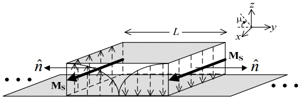
Cavity model of a patch at TM010 mode.
where W is the width of a patch antenna, ɛr is the permittivity of a substrate, S denotes the distance of the radiating slot to the far-field region, and μ represents the angle on the y-z plane (Fig. 1).
As shown in Fig. 1, the patch antenna can be represented by two equivalent magnetic current arrays. The SEP that does not consider mutual coupling was used to model radiation from the patch antenna. The SEP is expressed as follows:
Fig. 2 illustrates the geometry of a 1 × N patch array antenna and its equivalent magnetic current sources, which were used to calculate the array patterns of the antenna. Each patch antenna can be represented by two equivalent magnetic currents when a source with a magnitude and phase is applied to port of each antenna. The array patterns of the 1 × N antenna can be expressed as follows:
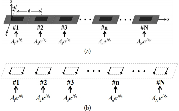
Calculation of array patterns using SEP. (a) Structure of an array antenna and (b) equivalent magnetic current of each patch.
where An and Φn are the magnitude and phase of the source applied to the nth antenna port.
Given the mutual coupling of space waves, higher-order waves, leaky waves, and surface waves [6], adjacent antennas radiate even though they are terminated with a matched load of 50 Ω [8]. Mutual coupling can be represented by an S-parameter with a magnitude and phase. Fig. 3(a) and (b) show the structure and equivalent magnetic current of the 1 × N array antenna, for calculating the AEPs of the nth patch. Power was applied to the nth patch antenna of the 1 × N array antenna, and the other antennas were terminated using 50 Ω. The antennas excited by mutual coupling are represented by equivalent magnetic currents. The solid and dotted arrows in Fig. 3 represent the magnetic currents due to applied power and mutual coupling.
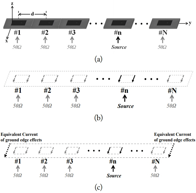
Calculation of AEPs. (a) Structure, (b) equivalent magnetic current of each patch, and (c) equivalent current of ground edge effects.
Mutual coupling between the antennas was adopted by the S-parameters obtained from the full-wave HFSS simulation. Determining the exact magnitude and phase of mutual coupling between patch antennas requires eliminating the influence of a feed structure. Accordingly, the reference plane of the S-parameters was removed from the port of the antenna. A coaxial feed can be calculated by considering the phase delay caused by the length of center conductor. After the phase delay is considered, the S-parameter matrix is represented by
Diagonal components {S11, S22, …, SNN} in [S] implies insertion loss due to the reflection of each port. To determine the magnitude of a pure radiation field of the nth port, the law of conservation of energy was applied. The phase of a pure radiation field was also obtained on the basis of boundary conditions 1 + Γ = τ. The diagonal components can be converted into Snn’ using the following equations:
The other off-diagonal components, {|S1n|ej∠S1n, |S2n|ej∠S2n, |S3n|ej∠S3n, …, |SNn|ej∠SNn}, correspond to mutual coupling. Thus, the AEP derived using the S-parameters is
This AEP is similar to the calculation result for an array antenna with a non-uniform magnitude and phase. By replacing the SEP with the AEP in Eq. (3), the array patterns of the 1 × N antenna for which mutual coupling is considered can be calculated thus:
In Eq. (8), the effects of the ground plane are disregarded. For an antenna with an actual ground plane, ground edge effects should be included in AEP calculation.
III. Array Pattern Analysis using Active Element Patterns with Ground Edge Effects
Precisely calculating the AEPs of a patch array requires the consideration of ground edge effects. In particular, the edge diffraction effects due to the surface waves in TM0 mode generated in the direction of the E-plane are dominant [6]. Fig. 3(c) shows the radiation model, with edge diffraction included. The surface waves reach the edge of the ground plane across the grounded dielectric plate and are diffracted. The edge diffraction can be explained by the following equation using GTD [10]:
where Einc is the edge’s incident wave stemming from surface waves; Einc is obtained by considering the propagation of surface waves in Eq. (1); βsurf denotes the propagation constant of surface waves, which is obtained using a dielectric slab model [11]; di indicates the distance of the radiating slot to the left edge when i = 1 and to the right edge when i = 2; and Dh represents the hard-boundary diffraction coefficient given in [10].
In Eq. (10)Edn is the edge-diffracted field from left and right radiating slots. The left and right superscripts indicate the edges of the left and right ground planes, respectively. The items within the square brackets constitute the equivalent radiation model of the antenna, which includes ground edge effects in calculation.
In general, the radiation patterns of an antenna are expressed as normalized [9], but using the array patterns obtained by adding each normalized pattern is inaccurate. The gain patterns of AEPs can be obtained using [5]
Finally, the array patterns that include the edge effects of the ground plane can be calculated in the same manner as that indicated in Eq. (8). Fig. 4 summarizes the procedure for calculating array patterns.
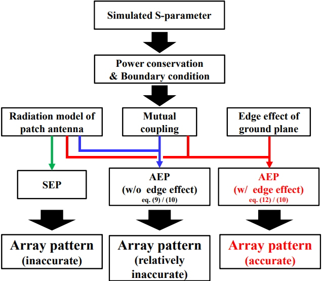
Flow chart of array pattern calculation.
IV. Calculation Results for Array Patterns
An array was designed on a Rogers RT/duroid 5880 (lossless) substrate with ɛr = 2.2 and h = 1.6 mm. The operating frequency was 5.8 GHz. Only the E-plane pattern was calculated given that the array antenna was of 1 × N type. The results for the AEP and array patterns were plotted on a linear scale to distinguish differences in detail.
Fig. 5 compares the AEPs calculated using Eqs. (7) and (10) with the HFSS- and FEKO-simulated AEPs of the 1 × 2 array antenna with array distances of 0.4λ0, 0.6λ0, 0.8λ0, and 1.0λ0 (Note that the width in the x-direction was fixed at 0.6λ0). In all the cases, the results with ground edge effects are more accurate than those without ground edge effects. At an array distance of 0.4λ0, the main lobe direction of the calculation results with ground edge effects is the same as that of the simulation results. Conversely, the main lobe direction of the calculation results without ground edge effects differs from that of the simulation results. The calculation results without ground edge effects have some errors in the size of the main lobe compared with the full-wave simulation results. Because the distance of the radiating slot of the antenna to the edge of the ground plane are close to each other (about 0.05λ0), higher-order mode effects were disregarded in our model [6].
AEP comparison of antenna #1 in the 1 × 2 array: (a) d = 0.4λ0, (b) d = 0.6λ0, (c) d = 0.8λ0, and (d) d = 1.0λ0.
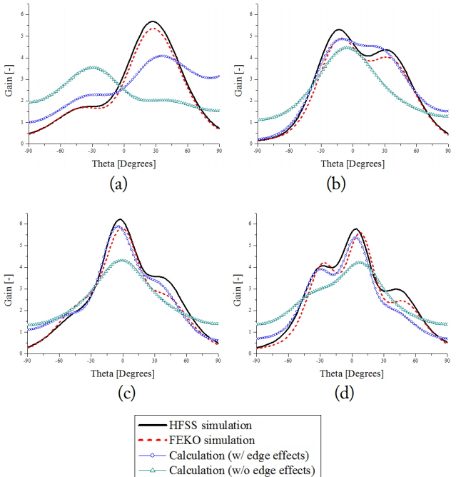
The calculation results for the 1 × 4 array antenna at array distances of 0.6λ0 and 0.8λ0 are shown in Fig. 6. Given that the structures of array antennas 1 & 4 and 2 & 3 are symmetrical, only the results for AEP 1 and 2 are shown, respectively. Because of the asymmetry in feed point, the asymmetry of the E-field in the left and right radiating slots of the patch is excited, thereby causing side-lobe error to occur at around 50°. Employing the symmetrical feed of the antenna in the full-wave simulation confirmed a reduction in side-lobe error.
AEP comparison for the 1 × 4 array. (a) Antenna #1 and (b) antenna #2 at d = 0.6λ0. (c) Antenna #1 and (d) antenna #2 at d = 0.8λ0.
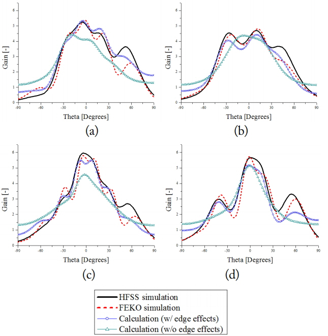
Fig. 7 illustrates the results of array pattern calculation at an array distance of 0.6λ0. The array patterns were calculated under various numbers of array elements at steering angles of 0°, 20°, and 40° (Note that a linear scale was used). In the case of the 1 × 2 and 1 × 4 antennas, which have a small number of arrays, the array patterns that include ground edge effects (circular elements in Fig. 7) more appropriately fit the HFSS and FEKO results (solid and dotted lines in Fig. 7, respectively) than do the array patterns that do not include ground edge effects (triangular elements in Fig. 7). In the case of the 1 × 16 antenna, which has a large number of array elements, the array patterns that include ground edge effects are similar to those without ground edge effects. Table 1 presents the calculation errors with respect to the results of the HFSS for different numbers of array elements and steering angles. The findings indicated that the errors in the calculation results with ground edge effects are constantly smaller than the errors in the calculation without ground edge effects.

Comparison of array patterns at steering angles of 0°, 20°, and 40° and an array distance of 0.6λ0: (a) 1 × 2, (b) 1 × 4, and (c) 1 × 16.

Calculation errors as determined on the basis of the HFSS results
According to the results, including the ground edge effects improve calculation accuracy in situations characterized by a small number of array elements. As surface waves propagate and reach the edge of the ground plane, its magnitude at the edge attenuates to 1/ρ1/2. The array elements located far from the edge do not contribute to the edge diffraction field. Thus, the proportion of array elements that do not interact with the edge diffraction field increases when the number of elements are large, indicating that the ground edge effects are not significant.
Another interesting observation is that the ground edge effects are important under a large steering angle. The field intensity of edge diffraction is small at the zenith direction (θ = 0°) and increases as angle θ increases [10]. Contrastingly, the magnitude of AEPs without ground edge effects is larger at the zenith direction (θ = 0°) and smaller as angle θ increases. For this reason, the ground edge effects are relatively small at a steering angle of 0° but expand as steering angle increases.
V. Conclusion
AEPs that include finite ground edge effects were precisely derived using S-parameters. Array patterns were then calculated using the computed AEPs and compared with simulation results. The findings indicated that the array patterns calculated on the basis of the AEPs that include ground edge effects are more accurate than those derived using the conventional AEP technique. Including the ground edge effects improve calculation accuracy particularly when the number of array elements is small. This importance is attributed to the addition of a relatively large edge diffraction field to a relatively small AEP magnitude at a large steering angle.
Acknowledgements
This research was supported by Basic Science Research Program through the National Research Foundation of Korea (NRF) funded by the Ministry of Education (No. 2015R1A6A1A03031833), and this research was supported by the Ministry of Science, ICT and Future Planning, Korea, under the Information Technology Research Center support program (No. IITP-2017-2016-0-00291) supervised by the Institute for Information & Communications Technology Promotion (IITP).
References
Biography
Sun-Gyu Lee received B.S. and M.S. degrees in electronic and electrical engineering from Hongik University in Seoul, Korea in 2016 and 2018, respectively. He is currently working toward a Ph.D. degree at the same institution. His research interests include phased array antennas and metasurfaces.

Jeong-Hae Lee received B.S. and M.S. degrees in electrical engineering from Seoul National University in Korea in 1985 and 1988, respectively, and a Ph.D. degree in electrical engineering from the University of California, LA in 1996. From 1993 to 1996, he was a visiting scientist of general atomics in San Diego, CA, where his major research initiatives were developing a millimeter-wave diagnostic system and studying plasma wave propagation. Since 1996, he has been working at Hongik University in Seoul, Korea as a professor in the Department of Electronic and Electrical Engineering. He has more than 100 papers published in journals and 60 patents. He is currently a vice president of the Korea Institute of Electromagnetic Engineering and Science and a director of the Metamaterial Electronic Device Center. His current research interests include metamaterial radio frequency devices and wireless power transfer.