Compact 28 GHz Folded Butler Matrix Using Low-Temperature Co-fired Ceramics
Article information
Abstract
This paper introduces a miniaturized Butler matrix design method using a folded structure. The Butler matrix was fabricated in multi-layers using low-temperature co-fired ceramics (LTCC) and designed to operate at 28 GHz. The conventional one-plane Butler matrix has a major disadvantage in that the length and volume of the system inevitably have to be increased. By using the proposed folded structure, the length can be reduced more than two times compared to the general one-layer Butler matrix. In order to minimize the loss of the Butler matrix, it was designed in a stripline structure by forming a ground plane on the upper and lower surfaces of each layer. A signal is transmitted between the layers through via holes. A 4 × 4 Butler matrix was fabricated and measured for the demonstration of the proposed concept. The proposed Butler matrix was measured through a precisely calibrated antenna chamber with closed cell absorbers. The dimensions of the fabricated Butler matrix are 14 mm × 20 mm × 1.52 mm. The beam of the fabricated Butler matrix can be properly steered in a total of four directions.
I. Introduction
Recently, the demand for and research on a mmWave wireless communication system that uses low-latency, high-quality data is increasing.
In the mmWave frequency band, a wide bandwidth can be used and is advantageous for large data transmission. However, the signal attenuation is very large compared to the low-frequency band. Therefore, it is necessary to use beamforming technology. The signal sensitivity between the transmitter and receiver can be maximally improved through beam steering.
The Butler matrix is an array antenna beamforming network, and it can steer the beam only with a switch without using a variable phase shifter. This is a well-known structure, and it is easy to design, since it can be implemented on a common printed circuit board [1, 2]. For example, in the case of a 4 × 4 Butler matrix, the beam can be steered in a total of four directions. In this structure, four hybrid couplers, two crossovers, and two delay lines are required. When the Butler matrix is designed as one layer, the length of the system increases because the aforementioned components must be connected in series.
Fig. 1 shows a conventional Butler matrix structure. The length of the system is visibly large because hybrid couplers, crossovers, and delay lines are all connected in series, including the array antenna. Additionally, it is difficult to reduce the size by removing or integrating components.
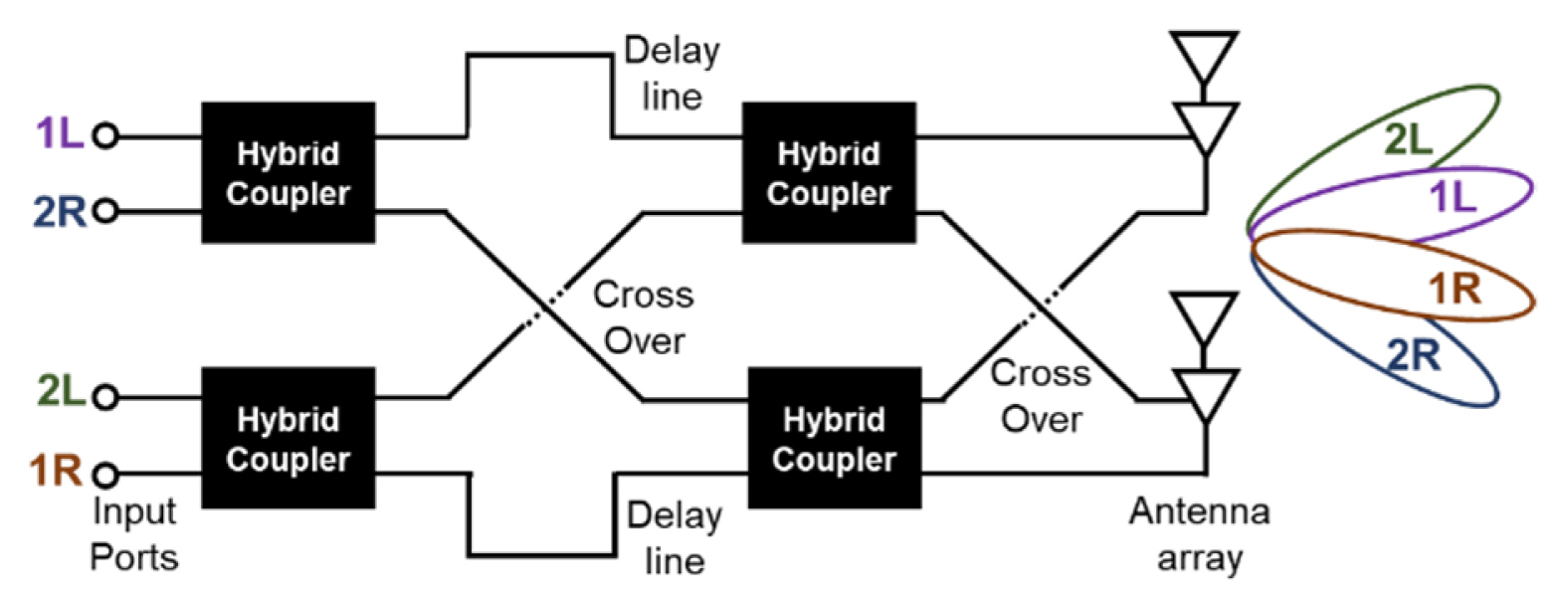
Conventional 4 × 4 Butler matrix.
In this paper, we propose a new topology that can reduce the size of the Butler matrix without removing or modifying components, such as couplers, shifts, and crossovers. To realize the proposed topology, a Butler matrix was implemented with a multi-layer substrate using low-temperature co-fired ceramics (LTCC). To verify the proposed structure, a 4 × 4 Butler matrix operating at 28 GHz was fabricated and measured.
II. Concept and Design
Fig. 2 shows the topology of the proposed folded multi-layer Butler matrix. As shown in Fig. 2, three layers are used and two hybrid couplers are located on Layer 1. Layer 2 has delay lines and a crossover. Signals can pass to other layers through via holes. The last two hybrid couplers and the crossover of the Butler matrix are on Layer 3. The array antenna may be designed by being located in Layer 3, where the last-stage hybrid coupler exists. However, in this paper, the array antenna was placed on Layer 2 to maintain its vertical symmetry. If the array antenna is asymmetrical, the radiation pattern is also formed asymmetrically. By using the proposed topology, the length of the Butler matrix can be greatly reduced.
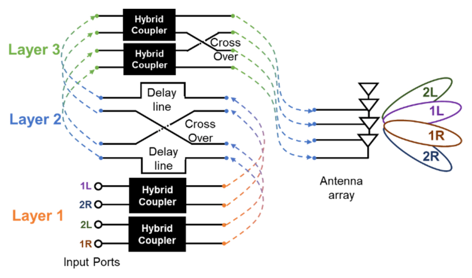
Proposed folded Butler matrix topology.
To design the Butler matrix, passive circuits, such as hybrid couplers, crossovers, delay lines, and the array antenna, must be individually designed. Fig. 3 shows the hybrid coupler structure and simulation results. The height of the substrate is 0.5 mm, and the thickness of the stripline is 0.01 mm. The substrate used in this work is Dupont, and the permittivity is about 7.5 at a frequency of 28 GHz. It was designed by a well-known hybrid coupler design theory, and it can be seen that the phase difference between port2 and port3 is about 90°.
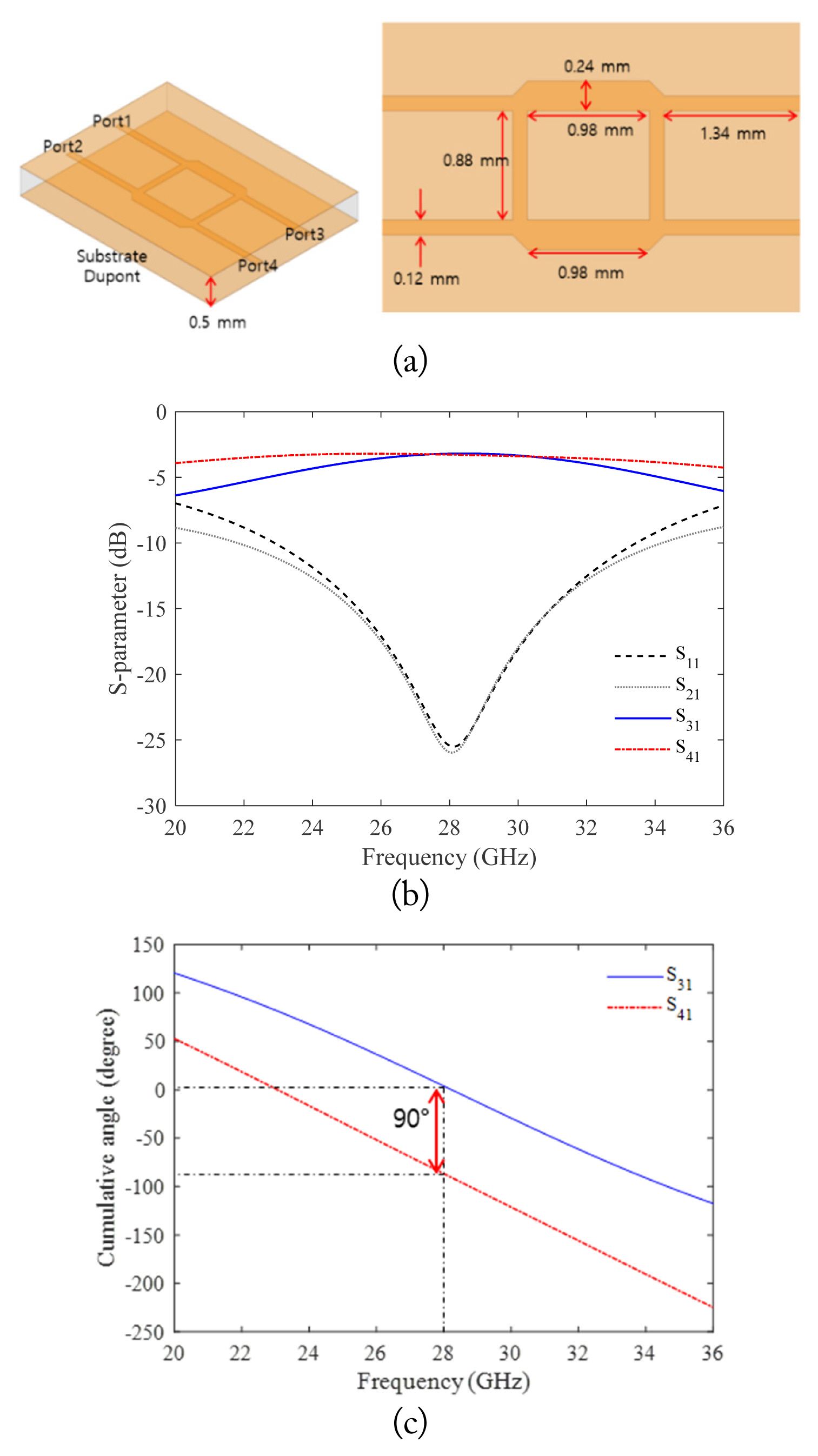
Hybrid coupler design: (a) physical dimensions, (b) simulation results, and (c) phase difference between port3 and port4.
Fig. 4 shows the crossover structure used in this work and the simulation results. Since the LTCC structure is used in this work, the crossover can be designed in multi-layers. In other words, it is easy to transmit a signal to another layer through a via hole. By using via holes, the port1 signal goes to port4 and the port2 signal goes to port3. Since the length of the transmission line between port1 and port4 and the same between port2 and port3 are different, a delay line is added to compensate for this difference. As shown in Fig. 4(b), the insertion loss is about 0.3 dB at 28 GHz, and it can be seen that it is well matched.
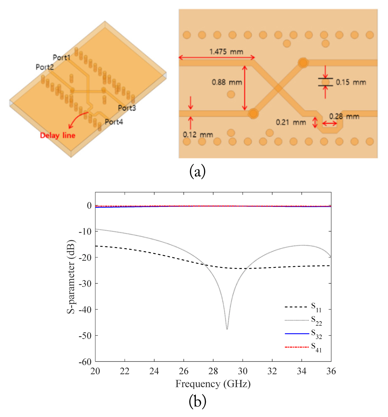
Crossover design: (a) physical dimensions and (b) simulation results.
Using the proposed topology and layer-to-layer transition by via holes, any type of planar Butler matrix can be miniaturized. Furthermore, Fig. 5 shows a conventional example and the proposed structure. The hybrid couplers in the first stage are placed on the first (lower) layer. Next, the delay line and crossover structure are designed on the second layer. In this case, a via hole is used to connect the first layer with the second. Additionally, there is no need to redesign structures, such as hybrid couplers and delay line crossovers. In this way, the size can be minimized by locating the elements on different layers.
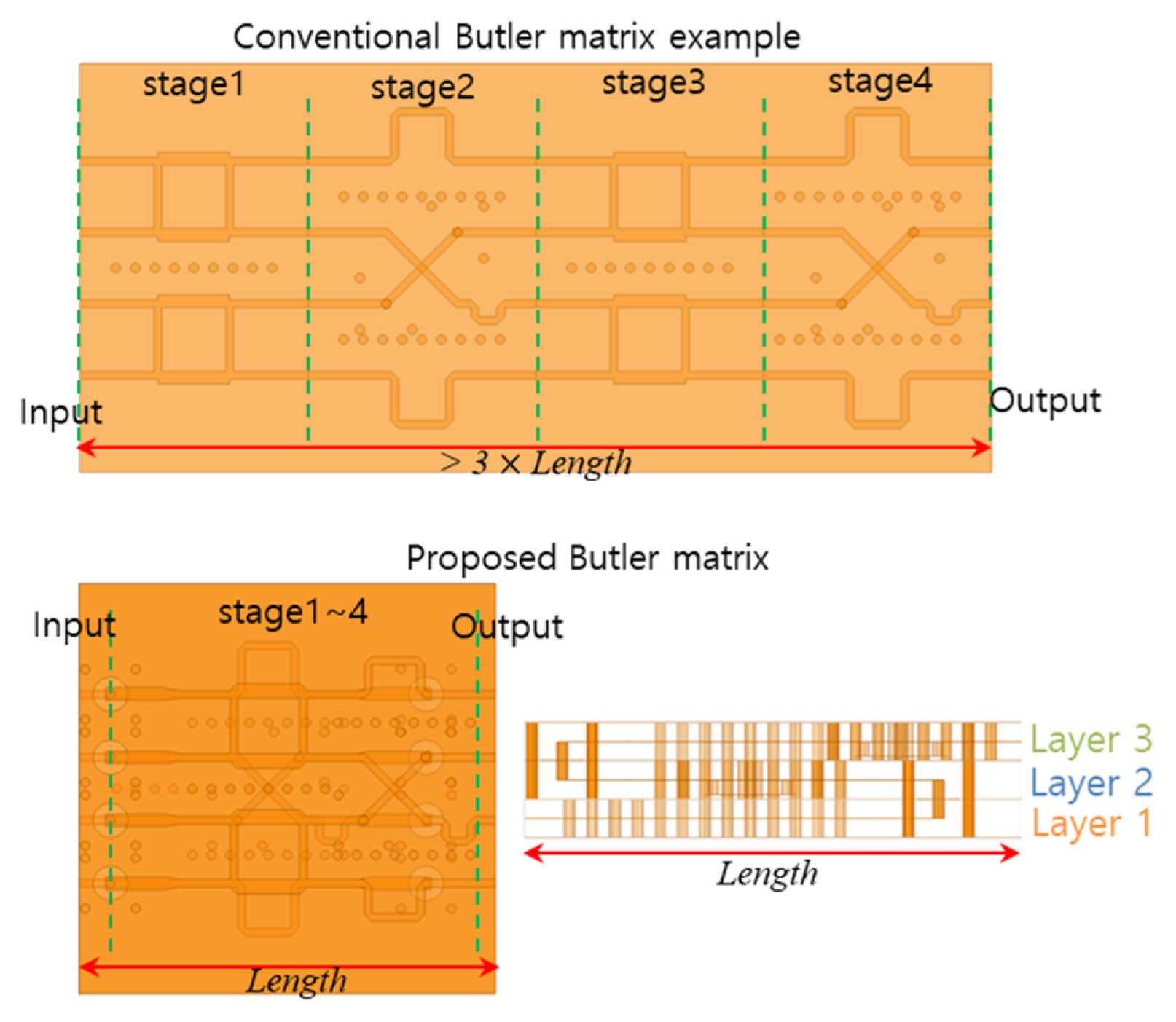
Example of a conventional Butler matrix structure and the proposed Butler matrix structure.
Next, in this paper, a monopole antenna for the Butler matrix was designed for proof of concept. As mentioned in the previous section, the monopole antenna was placed in the middle layer for vertical symmetry (on the z-axis). However, it is still an asymmetric structure on the x-axis. Fig. 6 shows a typical monopole antenna, a slant monopole antenna, and the corresponding radiation pattern. As shown in Fig. 6(a), a conventional monopole antenna is asymmetric on the x-axis, and when substrates with a high dielectric constant exist around it, the radiation pattern is tilted.
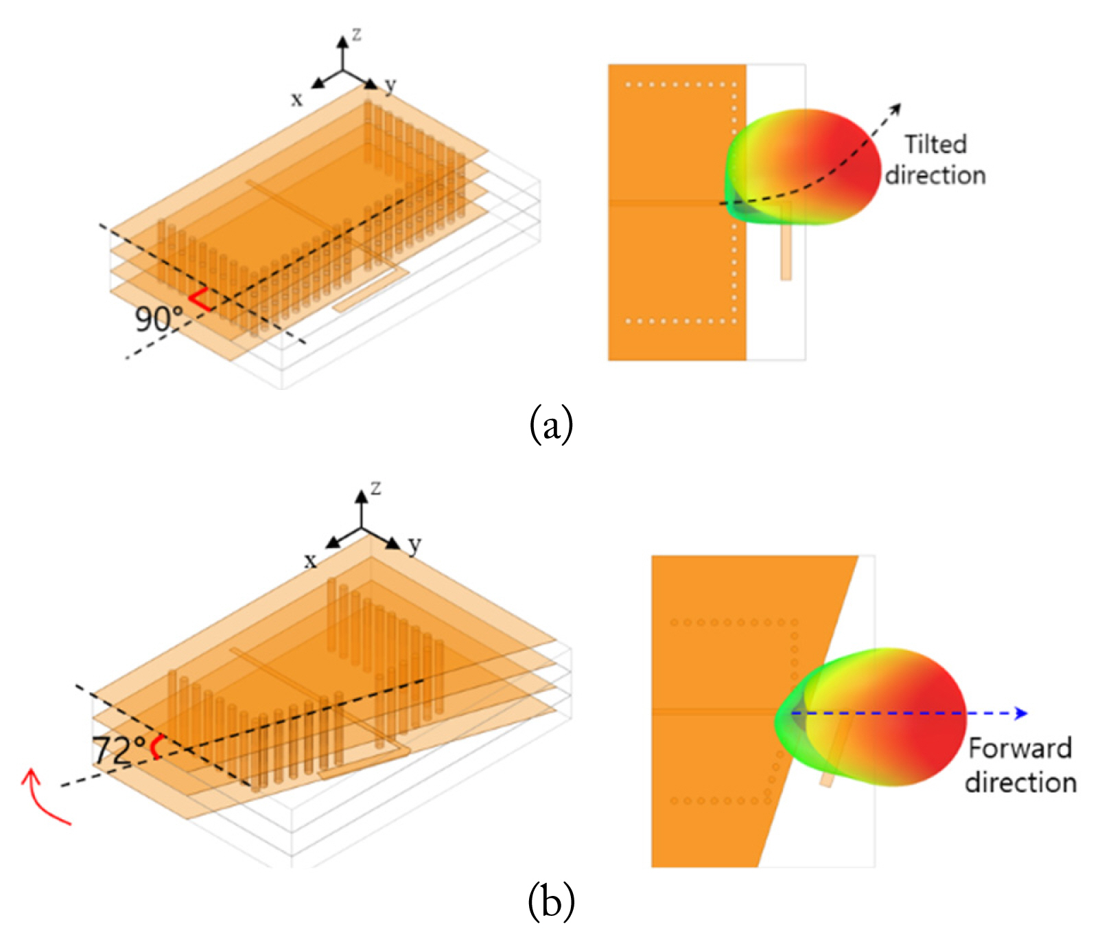
Monopole antenna structures and beam pattern: (a) normal model and (b) slant model.
To solve this problem, the monopole antenna and ground are designed in an oblique direction, as shown in Fig. 6(b). It can be seen that the radiation pattern is correctly formed in the forward direction—that is, the proposed monopole antenna has both vertical and horizontal symmetrical radiation patterns. The radiation pattern of the single antenna must be formed correctly so that the beam can be properly steered with the array antenna later. Since the ground acts as a reflector, the direction of the radiation pattern can be adjusted. The detailed radiation pattern is in [3].
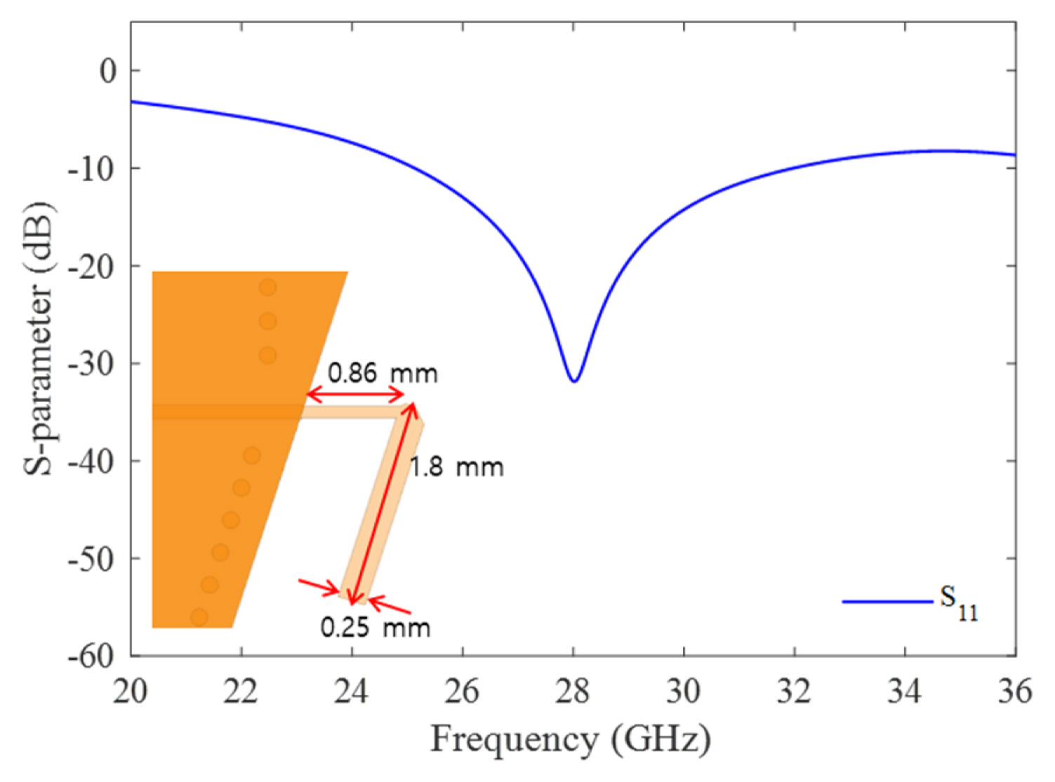
Moreover, Fig. 7 shows the physical dimensions and S-parameter simulation results of the proposed slant monopole antenna structure. At the target frequency of 28 GHz, it can be seen that S11 has a value of about −30 dB.
Simulation result of the monopole antenna.
Fig. 8 shows the radiation pattern of the proposed slant monopole antenna. The gain of a single antenna is about 4.7 dBi at 28 GHz. Considering the frequency and antenna size, this is an appropriate gain value compared to other works [4, 5]. Fig. 9 shows the radiation pattern of the proposed array antenna during beam steering. The distance between the antennas was set to 5 mm. Then, the simulation was performed by adjusting the phase difference used in the general Butler matrix. It was confirmed that the beam could be steered in the desired direction.

Radiation pattern of the slant monopole antenna.
Radiation pattern of the proposed array monopole antenna.
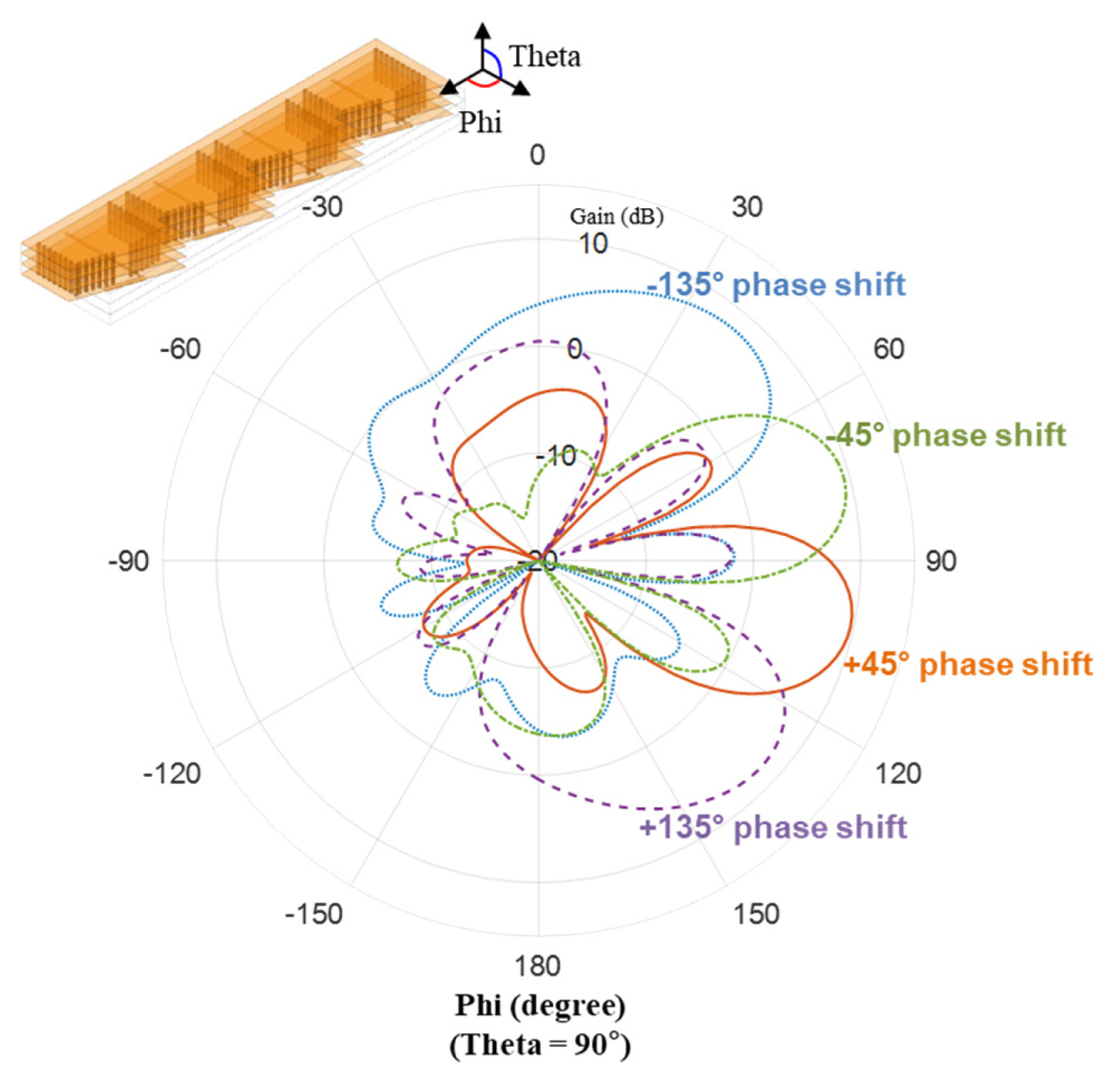
Next, the phase difference between the output ports was confirmed by simulating the Butler matrix without the array antenna. The Butler matrix should be simulated without the array antenna to accurately obtain the phase difference between the output ports. Fig. 10 shows the simulation structure and the phase difference between the output ports. According to the typical Butler matrix theory, it can be seen that the phase difference among S51, S61, S71, and S81 is about 45°. Similarly, the phase difference between S52, S62, S72, and S82 is about 135°. It should be noted here that since this structure is symmetrical, the phase difference between the remaining ports is omitted.
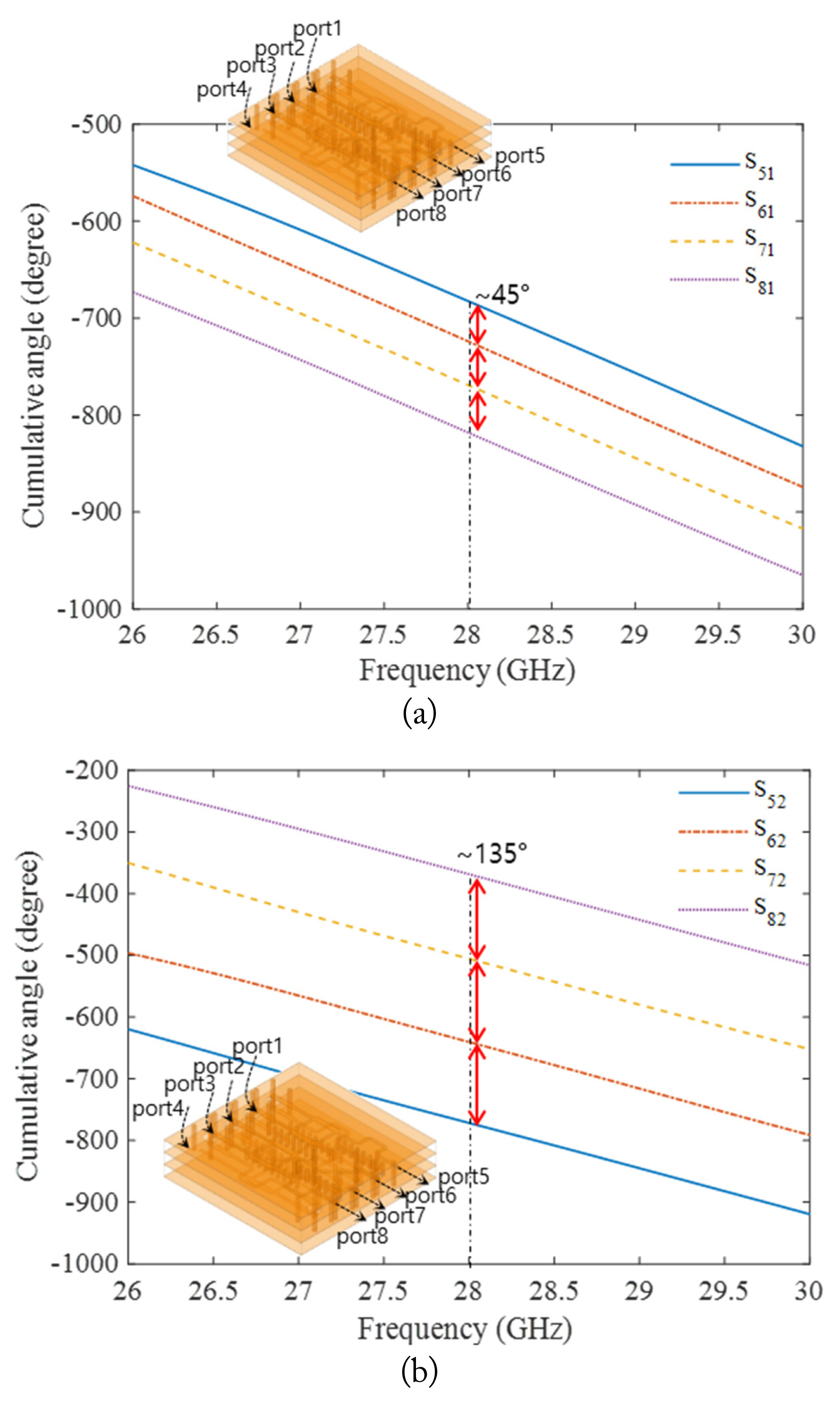
Simulation results of the Butler matrix without the array antenna: (a) phase difference (port1 to port5, port6, port7, and port8) and (b) phase difference (port2 to port5, port6, port7, and port8).
Since the length of the antenna’s feeding line of Layer 2 is different, the Butler matrix needs to be slightly modified, as shown in Fig. 11. In other words, the output reference plane of the Butler matrix needs to be moved and redesigned. The output reference plane can be adjusted by simply changing the length of the last delay line of the Butler matrix. In fact, only the delay line structure of the last stage needs to be modified.
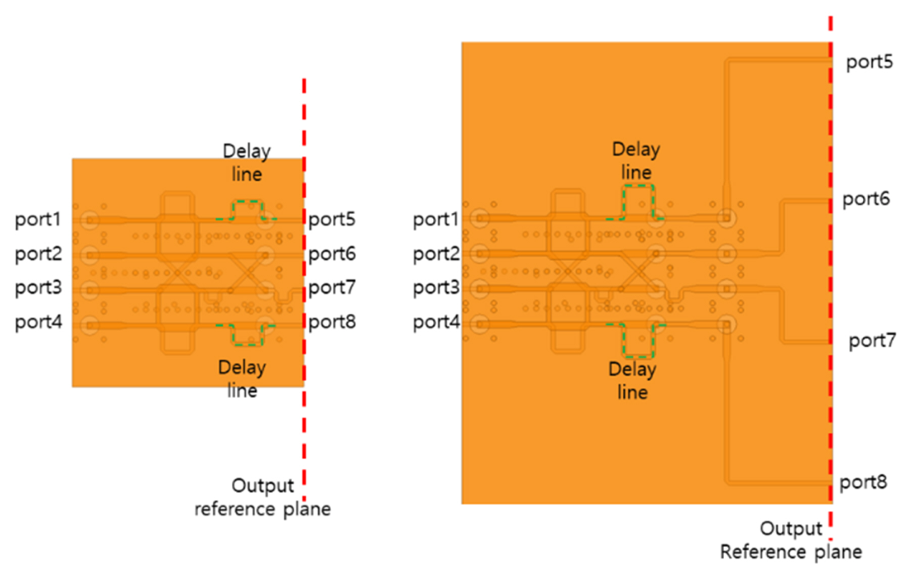
Modified Butler matrix for the antenna feeding line’s length compensation.
Fig. 12 shows a total layout view of the proposed Butler matrix. Since the Butler matrix made of LTCC is too small to be directly linked to the 2.92 mm connector, a test board for the connector attachment was designed. The test board was designed using a Rogers TMM10 substrate with a height of 0.508 mm and a dielectric constant of 9.2.
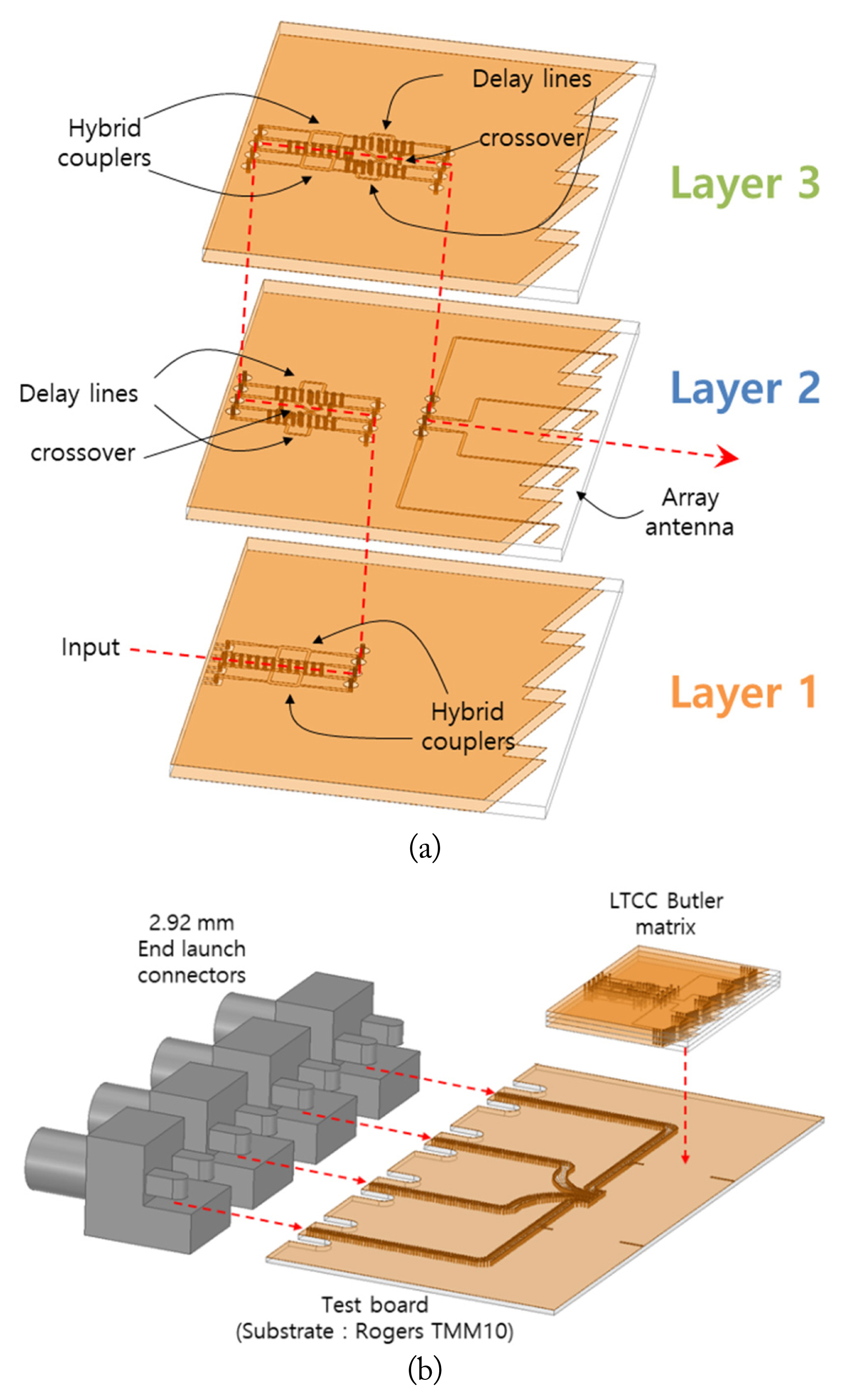
Total layout of the proposed Butler matrix: (a) layer-by-layer view and (b) connectors and the test board.
III. Measurement
To prove the proposed structure, the simulated structure was fabricated and measured. Fig. 13 shows the fabricated Butler matrix and the measurement setup. In this work, a 2.92 mm end launch connector (model 1092-01A-9; Southwest Microwave Inc., Tempe, AZ, USA) was used.
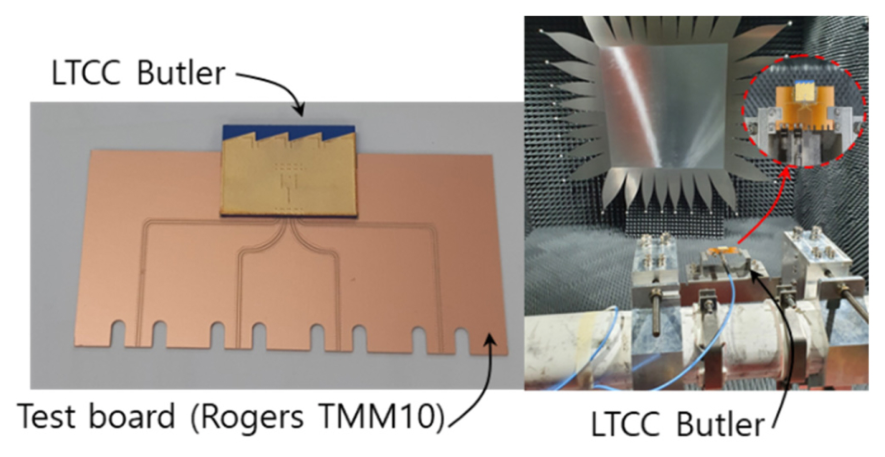
Fabricated Butler matrix and measurement setup.
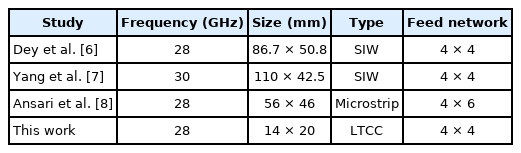
Fig. 14 shows the measurement results of the radiation pattern. The maximum array gain of the antenna is 5 dB. The average 3 dB beam angle is 24.8° (To elaborate, 26° at the port1 beam, 23° at the port2 beam, 26° at the port3 beam, and 24° at the port4 beam). When measuring the Butler matrix, unused ports were connected to a 50 Ω termination. The beam can be steered in desired directions. In addition, the measured and simulation results are almost identical. A small discrepancy seems to be caused by a manufacturing error, material composition, measurement error, simulation error, and so on. When measuring the gain, the loss of the test board and connectors was not excluded. Fig. 15 shows the measured results of cross-pol performance. The quantitative comparisons of similar studies are summarized in Table 1 for the convenience of our readers [6–8].

Measured radiation patterns of the fabricated Butler matrix.
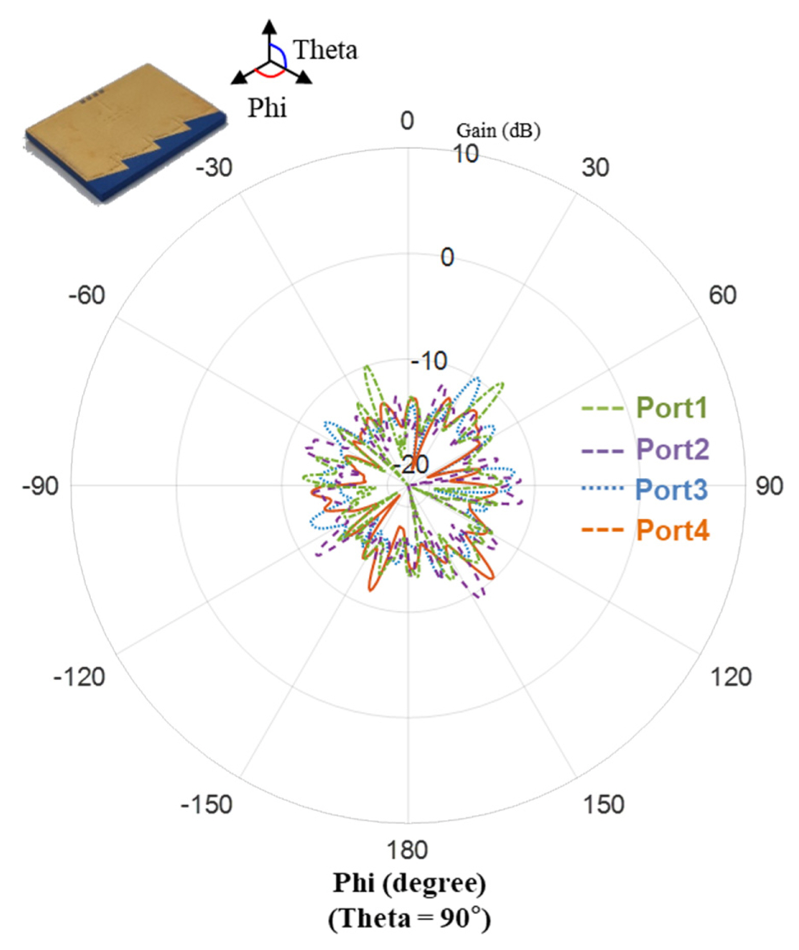
Measured results of cross-pol performance.
Comparison table
IV. Conclusion
In this paper, a compact 4 × 4 Butler matrix operating at 28 GHz is introduced. The proposed topology can greatly reduce the length of the Butler matrix with multi-layers using the LTCC technique. In this work, design parameters and substrate information are provided so that anyone can perform the same simulation. The proposed compact topology is suitable for 5G mmWave applications. This was verified through fabrication and measurement. As a future work, we will design a miniaturized 8 × 8 Butler matrix, and develop a structure that can minimize transition loss between layers.
Acknowledgments
This work was supported by the Technology Development Program (S3050488), which was funded by the Ministry of SMEs and Startups (MSS, Korea).
References
Biography

Seunggoo Nam received his B.E. degree in computer and communication engineering from Korea University, Seoul, Republic of Korea, in 2015. He received his Ph.D. in radio communications engineering from Korea University, Seoul, Republic of Korea, in 2020. In 2020, he joined Samsung Electronics, Suwon, South Korea, where he was involved in the design of a 5G mmWave front-end module. In 2021, he joined the Korea Electronics Technology Institute, Seongnam, South Korea, where he was involved in research activities focused on antennas, frequency tunable filters, and the convolutional neural network for deep learning. He is currently working as a Senior Researcher of ICT Device and Pack-aging Research Center. His current research interests include K-band frequency tunable filters, array antennas, and the 5G mmWave module.

Sehwan Choi received his M.S. degree in mmWave engineering from the Gwangju Institute of Science and Technology (GIST), Republic of Korea, in 2003. He received his Ph.D. in radio communications engineering from Hanyang University, Seoul, Republic of Korea, in 2017. In 2004, he joined the Korea Electronics Technology Institute, Seongnam, South Korea, where he was involved in research activities focused on antennas, front-end modules, and beamformers. He is currently the team leader of ICT Device and Packaging Research Center. His current research interests include the 5G passive beamformer, liquid crystal phase shifter, and reconfigurable intelligent surface.

Jongin Ryu received his B.S. and M.S. degrees in radio science and engineering from Hanyang University in 1998 and 2000, respectively. He received his PhD in electronic engineering from Hanyang University, Seoul, Korea, in 2019. From 2002 to 2006, he worked at Samsung Electronics, where he developed an RF modem IC application for GSM/GPRS/EDGE. In 2006, he joined the Korea Electronics Technology Institute (KETI). Following this, he developed the components of a cell phone, including FEM, dual-band PAM, LTCC module, radar, and antennas, among others. He is currently working as a Chief Researcher of ICT Device and Pack-aging Research Center. He is currently focusing on researching array antennas and the antenna-on-package module based on both LTCC and an organic substrate.

Jaeyoung Lee received his B.E. degree in electronic engineering from Ajou University, Suwon, Republic of Korea, in 1990 and M.E. degree in electronic engineering from Hanyang University, Seoul, Republic of Korea, in 1999. He received his Ph.D. in electronic and radio engineering from Kyung Hee University, Seoul, Republic of Korea, in 2016. In 1990, he joined LG Electronics in Osan, South Korea, where he was involved in designing the hybrid IC module. In 1996, he joined the Korea Electronics Technology Institute, Seongnam, South Korea, where he was involved in research activities focused on the ICT device module for mobile phones. He is currently working as a Chief Researcher of ICT Device and Pack-aging Research Center. His current research interests include military devices, such as radars, antennas, and RF modules, among others.