Performance of a Planar Leaky-Wave Slit Antenna for Different Values of Substrate Thickness
Article information
Abstract
This paper presents the performance of a planar, low-profile, and wide-gain-bandwidth leaky-wave slit antenna in different thickness values of high-permittivity gallium arsenide substrates at terahertz frequencies. The proposed antenna designs consisted of a periodic array of 5 × 5 metallic square patches and a planar feeding structure. The patch array was printed on the top side of the substrate, and the feeding structure, which is an open-ended leaky-wave slot line, was etched on the bottom side of the substrate. The antenna performed as a Fabry-Perot cavity antenna at high thickness levels (H = 160 μm and H = 80 μm), thus exhibiting high gain but a narrow gain bandwidth. At low thickness levels (H = 40 μm and H = 20 μm), it performed as a metasurface antenna and showed wide-gain-bandwidth characteristics with a low gain value. Aside from the advantage of achieving useful characteristics for different antennas by just changing the substrate thickness, the proposed antenna design exhibited a low profile, easy integration into circuit boards, and excellent low-cost mass production suitability.
I. Introduction
The terahertz (THz) regime, which spans the frequencies of 0.1–10 THz, is the least explored region of the electromagnetic spectrum. This regime is located between the microwave and the optical frequencies and has potential in emerging applications in sensing, imaging, and astronomy, among others. Its unique application in the screening of explosives, biohazards, and weapons and in envisioning concealed objects has also increased the worth of this band for researchers [1, 2]. Besides these applications, radiofrequency engineers suggest that the THz band can also be used to meet the demand of high data rates in wireless communication systems. This band offers many advantages, including extremely high data rate, wide bandwidths, better resolution, and improved spatial directivity with system compactness [3].
Lens-coupled antennas are widely used in the THz regime because of their advantages of high gain, wide bandwidth, mechanical rigidity, and thermal stability. However, these antennas have their intrinsic drawbacks of bulky size and low radiation efficiency due to the excitation of surface modes that occurs, especially when the substrate thickness is comparable with the excitation signal wavelength [4–6].
Fabry-Perot cavity antennas have also been proposed for THz radiation because of their promising properties of high gain, low complexity, and stability of fabrication, but these antennas undergo design challenges involving a low 3-dB gain bandwidth, particularly antennas with high-permittivity substrates [7–10]. The electrically thick substrates in the THz frequency cause serious problems, such as substrate resonance, which can be eliminated by decreasing the substrate thickness up to λo/20, where λo is a free space wavelength [11]. In recent years, researchers have demonstrated many extraordinary properties of metasurface antennas [12–17] because of their potential to provide the novel characteristics of an ultra-low profile and enhanced performance in gain, radiation pattern, and bandwidth [18]. Metasurface antennas have their own intrinsic advantages of easy fabrication, low cost, light weight, and extreme flatness.
In this work, we studied the performance of a planar leaky-wave slit antenna in different substrate thickness values to obtain the advantages of both Fabry-Perot cavity antenna and metasurface antenna characteristics just by changing the substrate thickness. The antenna consists of an array of square patches and a planar leaky-wave slit feeding structure etched on both sides of a high-permittivity gallium arsenide (GaAs) substrate. The patches printed on the top side of the substrate are a bidirectional periodic array of square patches, and the center-fed planar feeding structure is printed on the bottom side of the substrate. The antenna is optimized at each value of the substrate thickness for an optimum wideband gain bandwidth. This paper is organized as follows: the geometry and the modeling of the antenna are described in Section II. The characteristics of the antenna with respect to substrate thickness are discussed in Section III. The conclusions are presented in Section IV.
II. Antenna Geometry and Modeling
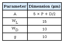
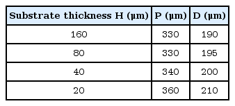
The detailed geometry of the proposed antenna is shown in Fig. 1. The antenna was patterned on both sides of the GaAs substrate (dielectric constant of ɛr = 12.9). As the GaAs material has a high breakdown field and a short carrier lifetime along with reasonably good mobility, it is considered one of the most suitable materials for the fabrication of photoconductive antennas. The patch array, consisting of symmetric bidirectional 5 × 5 metallic square patches, was patterned on the top side of the substrate. The width and the periodicity of the square patch array were defined as D and P, respectively. The feeding structure, an openended leaky-wave slit of width WL, was etched on the bottom side of the substrate. The metallic layer used in the ground plane and the patch array had a thickness of 0.35 μm and conductivity of 1.6 × 10⁷ S/m. The antenna had an overall dimension of A × A × H μm3, where A is the lateral size and H is the thickness of the substrate. The slit was fed by a short dipole at its center, which has a gap and a width of g and Wd, respectively. The substrate thickness H values varied from 20 μm to 160 μm. The antenna was optimized for each value of H (H = 20, 40, 80, 160 μm) by changing the periodicity and patch size while maintaining all the other design parameters. The optimized design parameters of the antenna to attain the optimum broadside gain and 3-dB gain bandwidth are summarized in Tables 1 and 2, respectively.
III. Antenna Characteristics
We modeled the antenna structure and investigated the characteristics of the antenna using the commercial electromagnetic wave simulator CST Microwave Studio (CTS Computer Simulation Technology GmbH, Darmstadt, Germany) based on the finite integration time domain technique. The antenna was excited by the default Gaussian-shaped signal in the desired frequency range by placing a discrete port in the dipole gap at the center of the slit line.
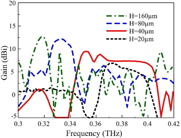
Fig. 2 shows the gain characteristics of antennas at different substrate thickness values. As the thickness, H, of the substrate decreased from H = 160 μm to H = 20 μm, the gain response shifted to higher frequencies. In fact, the change in the substrate thickness changed the effective permittivity. Thus, the gain response shifted to lower or higher frequency as the substrate thickness increased or decreased, respectively.
The antenna performed as a Fabry-Perot cavity antenna at a high thickness range, exhibiting high gain with narrow gain-bandwidths. Conversely, the antenna performed as a metasurface antenna at a low thickness substrate range and showed wide-gain-bandwidth characteristics, but the gain decreased with decreasing thickness. At thickness levels of H = 160 μm and H = 80 μm, the antenna presented similar gain values of 13 dBi and 12.5 dBi, respectively. The 3-dB gain bandwidth was narrow at 2% and 4.8% with respect to their central frequencies of 0.316 THz and 0.332 THz at H = 160 μm and H = 80 μm, respectively. The antenna with a substrate thickness of H = 40 μm exhibited wideband and stable gain characteristics, with a value of 9.8 dBi, and the 3-dB gain bandwidth was greater than 16% (0.34 – 0.4 THz). The antenna gain was around 7 dBi, and the 3-dB gain bandwidth was approximately 8% (0.365 – 0.395 THz) for the antenna with H = 20 μm. These results indicate that antennas with thick substrates produce high gain values and are thus suitable for applications requiring high gain. Antennas with thin substrates, especially those where H = 40 μm, are good candidates for applications that demand a wide bandwidth with moderate gain.
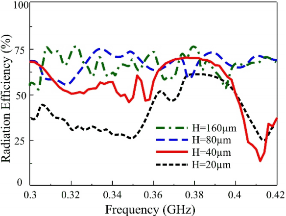
The radiation efficiencies of the antennas are shown in Fig. 3. The antennas with thick substrates achieved high radiation efficiencies, which decreased for antennas with thin substrates. The maximum radiation efficiencies verified within the 3-dB gain bandwidth was approximately 75% for antennas with H = 160 μm and H = 80 μm thickness levels. This value decreased to approximately 69% and 60% at H = 40 μm and H = 20 μm, respectively. Note that although the radiation efficiency was high for thick substrates, the antenna gain dropped to zero at some specific frequencies (e.g., around 0.35 and 0.38 THz). In fact, the antenna radiated well but not in the boresight direction, in which the antenna gain was calculated. Thus, the measured gain dropped to zero, even though the radiation efficiency was high.
Fig. 4 presents the radiation patterns of the antennas at their central frequencies. In general, all the antennas showed clean profile patterns with low side-lobe levels and back radiation in both the xz- and yz-planes, and the gain increased with the increase in substrate thickness. Antennas with thick substrates produced similar directive radiation patterns, with a narrow, half-power beamwidth (HPBW). The HPBWs were approximately 12° and 15° for antennas with substrates at H = 160 μm and H = 80 μm, respectively. An interesting phenomenon was observed for the antennas with thin substrates. The HPBW in the xz-plane increased while having a narrow HPBW in the yz-plane. The HPBWs in the xz-plane were 140.5° and 130° for H = 40 μm and H = 20, respectively. These values were around 30° in the yz-plane.

Radiation patterns of the antennas: (a) H = 160 μm at 0.316 THz, (b) H = 80 μm at 0.332 THz, (c) H = 40 μm at 0.37 THz, and (d) H = 20 μm at 0.38 THz.
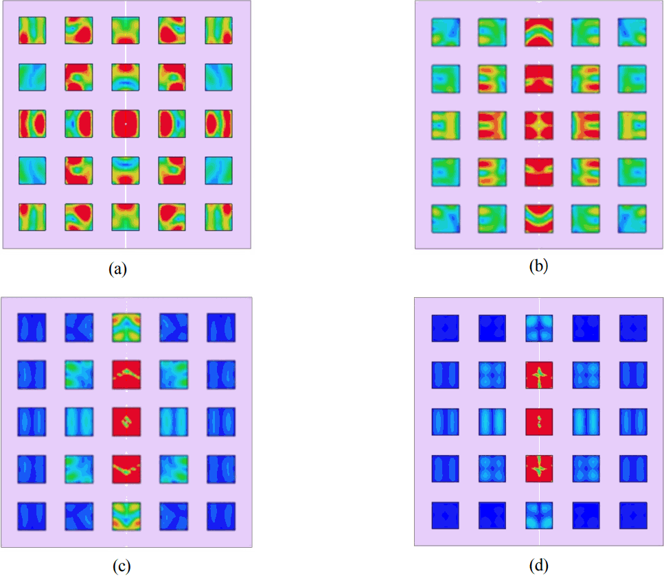
The surface current density in the patches was calculated to explain the radiation mechanism (Fig. 5). For thick values of the substrate, almost all of the patches were excited in all directions, producing symmetrical and directive radiation patterns with high gain values in both principal planes. In the case of the thin substrates, only the patches along the slit line were activated, and they had a strong current across the direction of the slit line (y-direction) that produced a strong field in the perpendicular direction. This outcome resulted in a wide beamwidth in the xz-plane, and the gain was limited because of the excitation of a few patches. Note that all the antennas showed low back radiation. Conventionally, the radiation pattern of the conventional slot in a thin substrate is bidirectional, and a back reflector is used to prevent this situation. However, a back reflector is not necessary in the proposed antenna design that employs a metasurface because of the effective coupling of the electromagnetic wave to the patch array from the leaky-wave slit feed. This coupling resulted in low back radiations.
IV. Conclusions
The characteristics of planar compact antennas with different substrate thicknesses were studied across the THz frequency range. Each antenna consisted of a square patch array of 5 × 5 and a planar feeding structure, both of which were patterned on a high-permittivity GaAs substrate. The antenna with a narrow 3-dB gain bandwidth at thick (H = 160 μm and H = 80 μm) values of substrate exhibited high gain. The antenna with thin substrates (H = 40 μm and H = 20 μm) produced low gain values but wide 3-dB gain-bandwidths. Therefore, the design enables the antenna to be adjusted for specific applications of high gain or wide-gain-bandwidth with moderate gain by simply changing the substrate thickness. Moreover, the antenna design provides a compact size, mechanical robustness, easy integration into circuit boards, and low-cost mass production suitability, which make the antenna a good candidate for applications in the THz frequency.
Acknowledgements
This work was supported in part by the Institute for Information & Communications Technology Promotion (IITP) grant funded by the Korea government (MIST) (No. 2017-0-00959, University ICT Basic Research Laboratory) and in part by the “Human Resources Program in Energy Technology” of the Korea Institute of Energy Technology Evaluation and Planning (KETEP), which was granted financial resource by the Ministry of Trade, Industry & Energy, Republic of Korea (No. 201640302-01380).
References
Biography

Niamat Hussain
received his B.S. degree in Electronics Engineering from Dawood University of Engineering and Technology, Karachi, Pakistan, in 2014. He is currently studying for his M.S. degree at the Department of Electrical and Computer Engineering at Ajou University, Suwon, Korea. His research is mainly focused on lens-coupled antennas, metasurface antennas, and terahertz antennas.

Kam Eucharist Kedze
received his Bachelor of Technology in Electrical and Electronic Engineering (Tele-communication) from the University of Buea, Cameroon, in 2013. He is currently studying for his M.S. degree at the Department of Electrical and Computer Engineering at Ajou University, Suwon, Korea. His research interest is the design of patch antennas, crossed-dipole antennas, and metasurface antennas.

Ikmo Park
received his B.S. degree in Electrical Engineering from the State University of New York at Stony Brook and his M.S. and Ph.D. degrees in Electrical Engineering from the University of Illinois at Urbana-Champaign. He joined the Department of Electrical and Computer Engineering at Ajou University in 1996. Prior to joining Ajou University, he was with the Device and Materials Laboratory, LG Corporate Institute of Technology, Seoul, Korea, where he was engaged in research and development of various antennas for personal communication systems, wireless local area networks, and direct broadcasting systems. He was a visiting professor at the Department of Electrical and Computer Engineering, Pohang University of Science and Technology, Pohang, South Korea, from 2004 to 2005, and at the Department of Electrical and Computer Engineering, University of Arizona, Tucson, AZ, USA, from 2011 to 2012. He has authored and co-authored over 300 technical journal and conference papers. He also holds over 30 patents. His current research interests include the design and analysis of microwave, millimeter-wave, terahertz wave, and nano-structured antennas. He is a member of the Board of Directors of the Korea Institute of Electromagnetic Engineering and Science. He is a member of Eta Kappa Nu and Tau Betta Pi. He served as Chair of the Department of Electrical and Computer Engineering at Ajou University. He serves as chair, organizer, and member of program committees for various conferences, workshops, and short courses in electromagnetic-related topics.

