I. Introduction
A substrate integrated waveguide (SIW), which has a form similar to a rectangular waveguide, was proposed by Deslandes and Wu [1], who implemented it by placing via holes in parallel on a printed circuit board (PCB). The SIW suffers from a greater loss than a conventional rectangular waveguide because the substrate is filled with a dielectric material and has dielectric loss, but it has the advantage of easy integration with planar active and passive devices. To compensate for the dielectric loss of SIW, a hollow substrate integrated waveguide (HSIW), which removes the dielectric material and uses air as the transmission medium, was proposed [2]. In several studies, low-loss HSIWs have been analyzed for application to directional couplers, filters, and antennas [3–5].
A power divider typically has two kinds of configurations: a corporate structure and a traveling-wave structure [6]. The number of ports into which a corporate power divider can split the input power is 2n because the power divider uses binary power dividers, such as the Wilkinson power divider, branch line power divider, Lange power divider, and rat race power divider. By contrast, a traveling-wave power divider can split the power into an arbitrary number of ports, thereby facilitating its usage.
In this paper, we propose a low-loss microstrip-to-HSIW transition using C-cut via holes and present a low-loss Ku-band 1:3 traveling-wave power divider, which is based on an HSIW structure and uses the proposed transitions. The microwave performance of the transition and the power divider is validated through electromagnetic simulations and measurements.
II. Microstrip-to-HSIW Transition
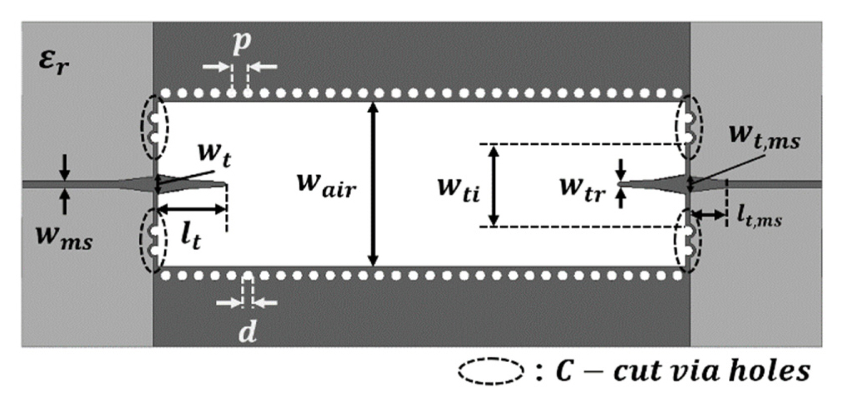
Active and passive planar devices are generally microstrip-type elements. A microstrip-to-HSIW transition is an essential component to reduce discontinuity at the interface of two different transmission structures. Fig. 1 shows the microstrip-to-HSIW transition proposed in this work. The proposed transition uses C-cut via holes that are symmetrically placed at the interface of the microstrip line and HSIW, thus reducing radiation and leakage effects through the shielding of via holes, and improving impedance matching. The C-cut via holes can be replaced with triangular, rectangular, or other geometric shapes, as the specific shape is not critical for microwave performance.
In Fig. 1, wms is the width of a 50 Ω microstrip line, d is the diameter of a via hole, and p is the distance between adjacent via holes. If d and p satisfy the conditions of (1) and (2), and the metallic loss is neglected, the radiation loss of two parallel via holes is less than 0.008 dB per wavelength. Therefore, the d and p values and the parameters of the C-cut via holes should be determined using (1) and (2) [7]. wt,ms, lt,ms, wt, lt, and wti are the design parameters, and their initial values are estimated from (3) to (7) [8]. lt,ms and lt determine the center frequency of the transition, and wt,ms, wt, and wti are related to the impedance matching and bandwidth. λg0 and λg,ms are the wavelength in free space and the guided wavelength of the microstrip line, respectively. The initial values of all the design parameters were calculated from the design equations and then optimized using electromagnetic simulations. Iterative optimization results in optimal design parameters for the bandwidth and return loss.
The microstrip-to-HSIW transition was designed using a 12 mil-thick RO4003C substrate provided by Rogers Corporation, Chandler, AZ, USA. The design goals are listed in Table 1, and the optimized geometrical design parameters are shown in Table 2. The bandwidth of the transition was intentionally set to 2 GHz, which is wider than that of the power divider for satellite communication systems, and an insertion loss of 0.6 dB was required for the power combining efficiency of 85%.
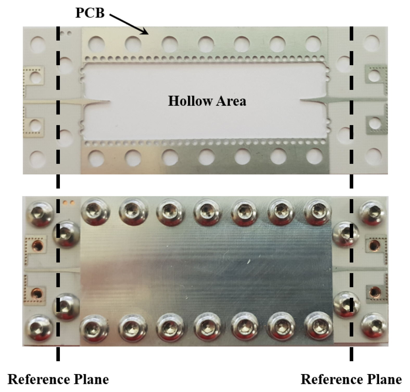
Fig. 2 is a photograph of the fabricated back-to-back microstrip-to-HSIW transition that occupies 55.5 mm × 30 mm (based on the reference planes). The top and bottom metal planes of the transition were implemented using top and bottom jig plates for convenience, although they could be fabricated using a conventional multi-layer PCB process.
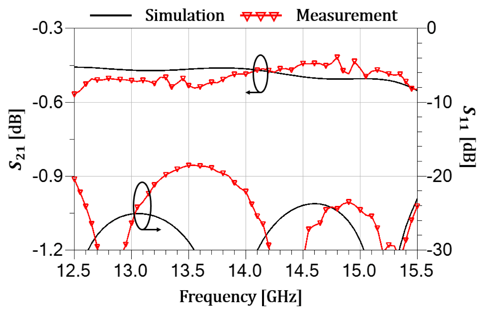
Fig. 3 compares the simulated and measured S-parameter results of the back-to-back microstrip-to-HSIW transition. The back-to-back transition had a return loss of 18 dB or more and an insertion loss of 0.5 ± 0.07 dB from 12.5 GHz to 15.5 GHz. The measured results were in good agreement with the simulated results, although the resonance notches of S11 slightly shifted to the lower frequency region by about 0.5 GHz.
III. Low-Loss Traveling-Wave Power Divider using HSIW and Microstrip-to-HSIW Transition
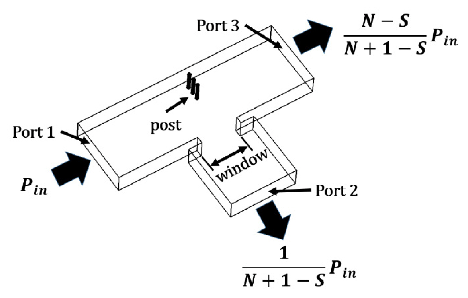
Fig. 4 shows a T-junction power splitter, which is conventionally used in a traveling-wave power-dividing configuration. For the traveling-wave power divider, a 1:N power divider requires (N–1) stages of the T-junction power splitters. In the schematic T-junction power splitter in Fig. 4, N is the total number of power-splitting ports, and S is the stage position number of the cascaded T-junction power splitters [9]. The power-splitting ratio in each port is also indicated.
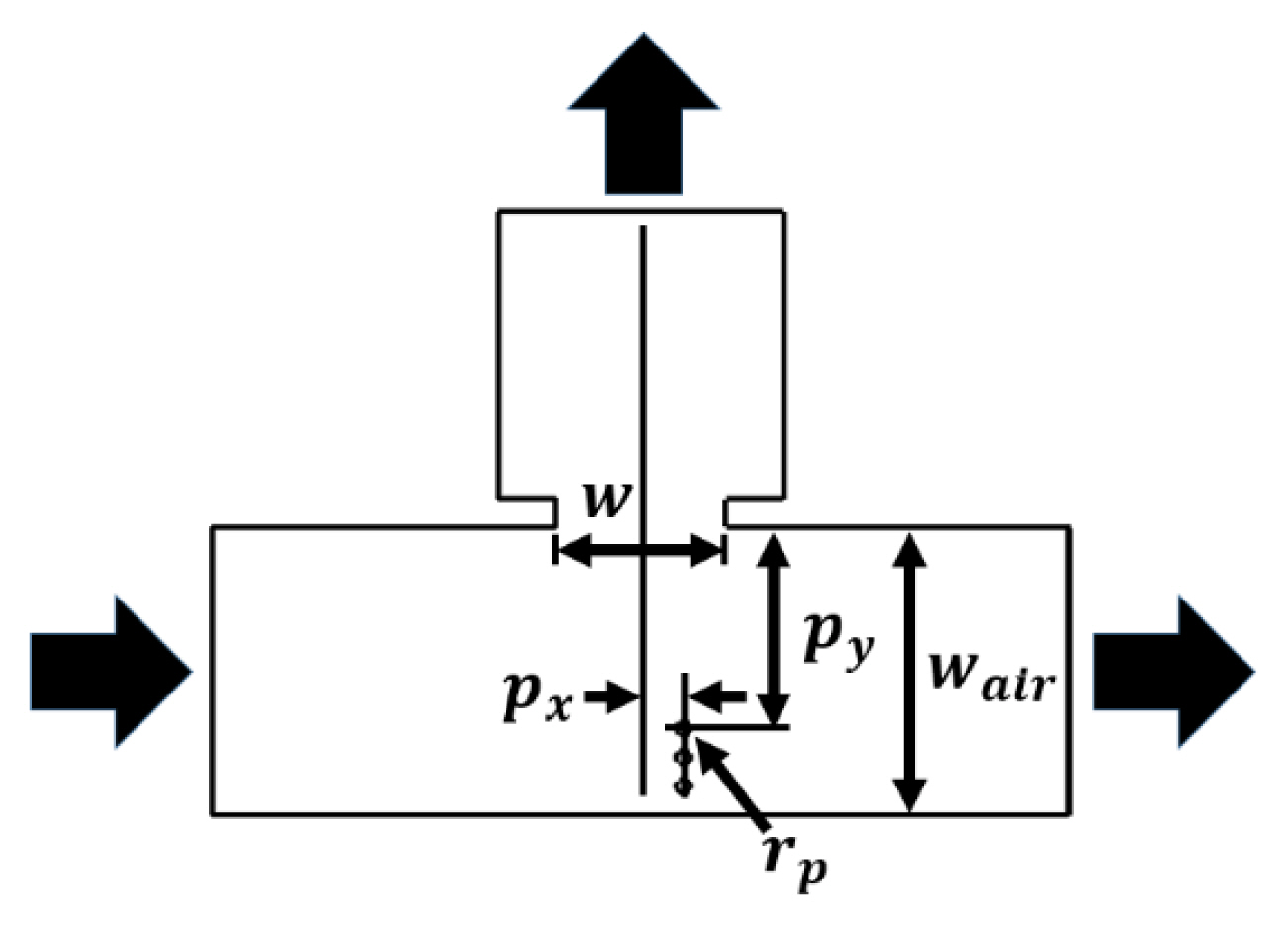
The design parameters of the T-junction power splitter are shown in Fig. 5, where w is the width of the window, px and py are the post position parameters, and rp is the radius of the post inserted near the T-junction. By tuning three main design parameters, namely w, px, and py, to determine an impedance matching condition and the desired power-splitting ratio, the optimal parameter values for the design goals can be obtained from electromagnetic simulations.
The design and optimization procedures for each power splitter are described as follows:
As the window width w is the most important parameter in Fig. 5, it should be designed and optimized to determine the center frequency and the power-dividing ratio.
After the window width w is determined, the post position of px is estimated and determined.
If the parameters w and px are optimized and the approximate performance is obtained, the post position of py is fine-tuned for optimal performance.
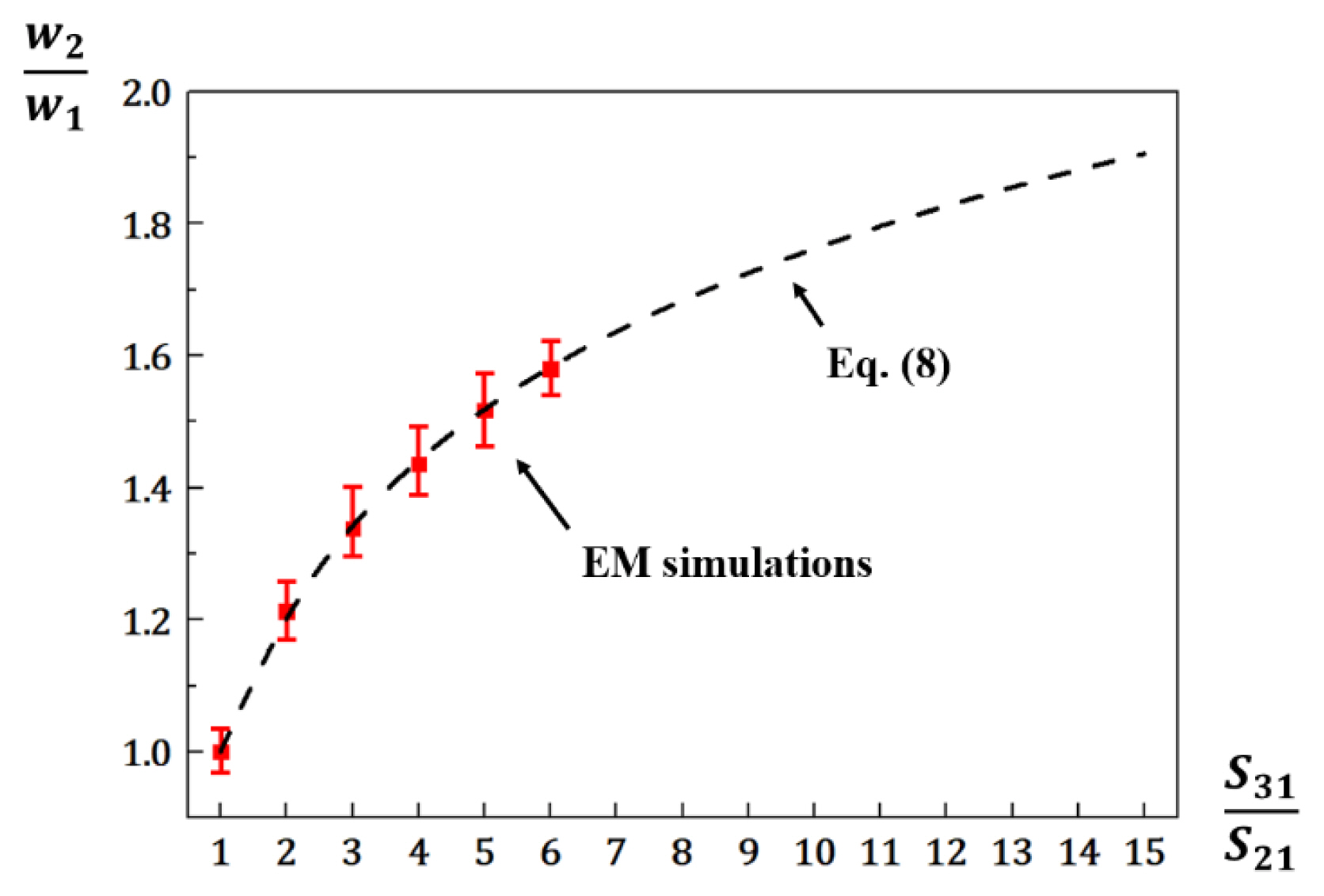
Fig. 6 shows two representative design parameters for the power-dividing ratio of the HSIW-based T-junction power splitter. The geometrical parameter w1 depends on the design center frequency, and the width ratio of w1 and w2 (w2/w1) mainly determines the power-dividing ratio of port 2 and port 3. The width ratio can be expressed as (8), which is shown as a dotted line, and it is compared with the symbols with y error bars in Fig. 7. The error bar symbols were calculated from 3D electromagnetic simulations and were in good agreement with (8).
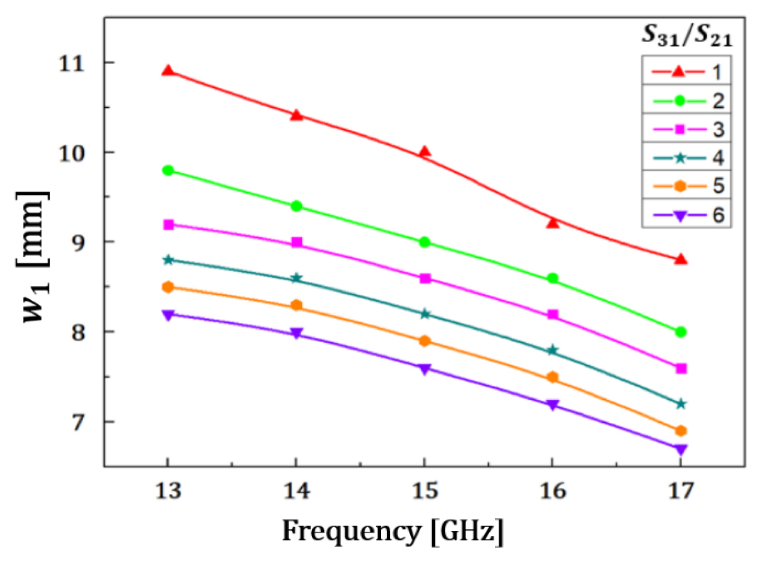
Fig. 8 shows w1 dependence on the frequency with varying power-dividing ratios of ports 2 and 3. w1 decreases with the dividing ratio, s31/s21, and the center design frequency. The HSIW-based T-junction power splitter was designed by extracting the initial values from (8) and optimizing them using electromagnetic simulations.
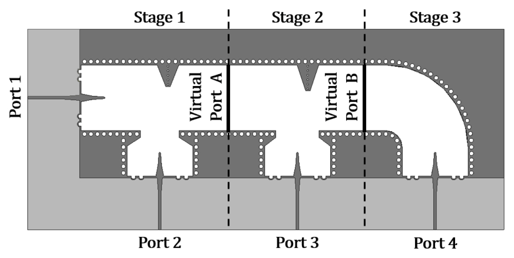
Fig. 9 shows the schematic diagram of our designed 1:3 traveling-wave power divider, which is based on an HSIW structure. To prevent the operating frequency shift and the deviation of the power-dividing ratio due to the transition, the transition in each port was included in the stage design process, and three designed stages were cascaded to complete the 1:3 power divider. First, we set the required power-dividing ratio for each stage and found the design parameter values for it from (3) to (8) and the electromagnetic simulations. The first stage (stage 1) had a ratio of 1:2, and the second stage (stage 2) had a ratio of 1:1. The last stage (stage 3) used a 90° curved bend, so that ports 2, 3, and 4 were on the same reference plane.
The Ku-band HSIW-based 1:3 traveling-wave power divider was designed using the RO4003C substrate, on which the microstrip-to-HSIW transition had been implemented. The design goals are listed in Table 3, and the optimized design parameters obtained from the simulations are shown in Table 4. As the back-to-back transition showed the measured insertion loss of 0.5 ± 0.07 dB, and as an additional path loss could be expected in the power divider, the insertion loss of 0.7 dB was set as the target value (Table 3), which corresponds to the power combining efficiency of 85%.
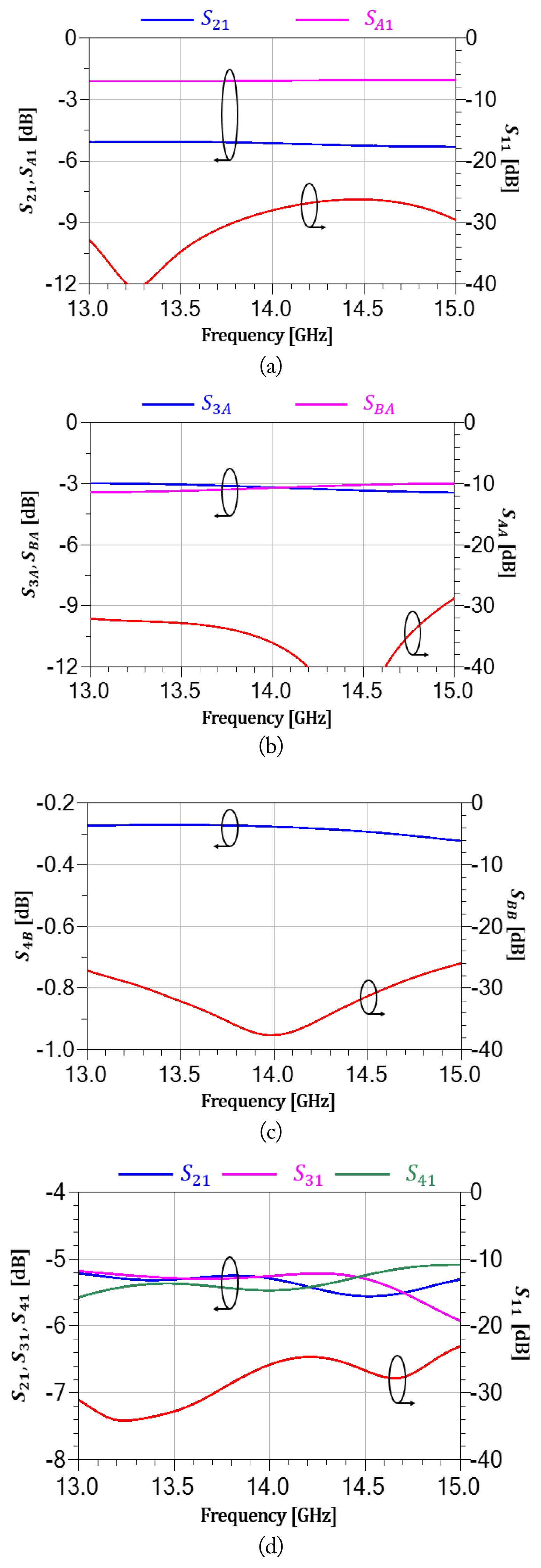
Fig. 10(a), (b), and (c) show the simulated S-parameter results for stages 1, 2, and 3, respectively. Fig. 10(d) shows the simulated results of the complete 1:3 power divider. Each designed stage had a return loss of 25 dB or more in the frequency range of 13.5–14.5 GHz and achieved the desired power-dividing ratios. The complete HSIW-based 1:3 power divider had a return loss of 24 dB or more and a transmission performance (S21, S31, S41) of –5.4 ± 0.15 dB from 13.5 GHz to 14.5 GHz. The frequency response of the power divider was somewhat narrower than that of each stage because the frequency bandwidth of the cascaded stages was typically narrower than that of a single stage. In the frequency range of 13.5–14.5 GHz, it had an insertion loss of about 0.57 dB and a power combining efficiency of 87.2% or more, which met our design goals.
IV. Fabrication and Measurement
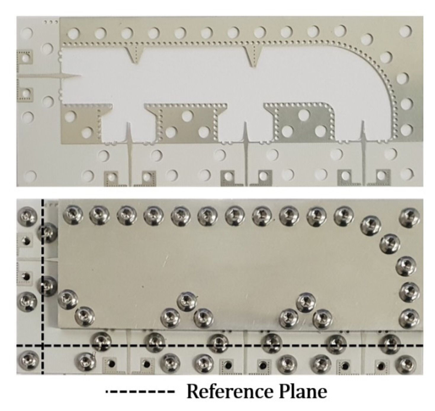
Fig. 11 shows the fabricated 1:3 traveling-wave power divider, the signals of which are divided in the HSIW structure. Estimated from the reference plane, the size of the power divider is 101.3 × 37.7 mm2, with the top and bottom metal planes formed using the jig itself after the PCB fabrication in the same manner as the microstrip-to-HSIW transition.
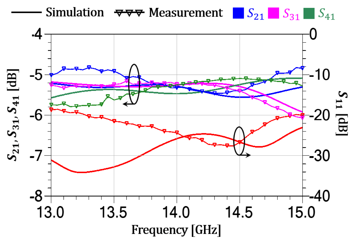
Fig. 12 compares the simulated and measured S-parameters of the HSIW-based 1:3 traveling-wave power divider. The measured results showed that the power divider had a return loss of 21 dB or more and a power-dividing ratio of –5.3 ± 0.3 dB in the frequency range of 13.5–14.5 GHz. The range of the power-dividing ratio widened slightly because of the PCB process tolerance. Our simulation showed that the proposed power divider in this work was somewhat sensitive to the width of the window and the post positions in Fig. 5.
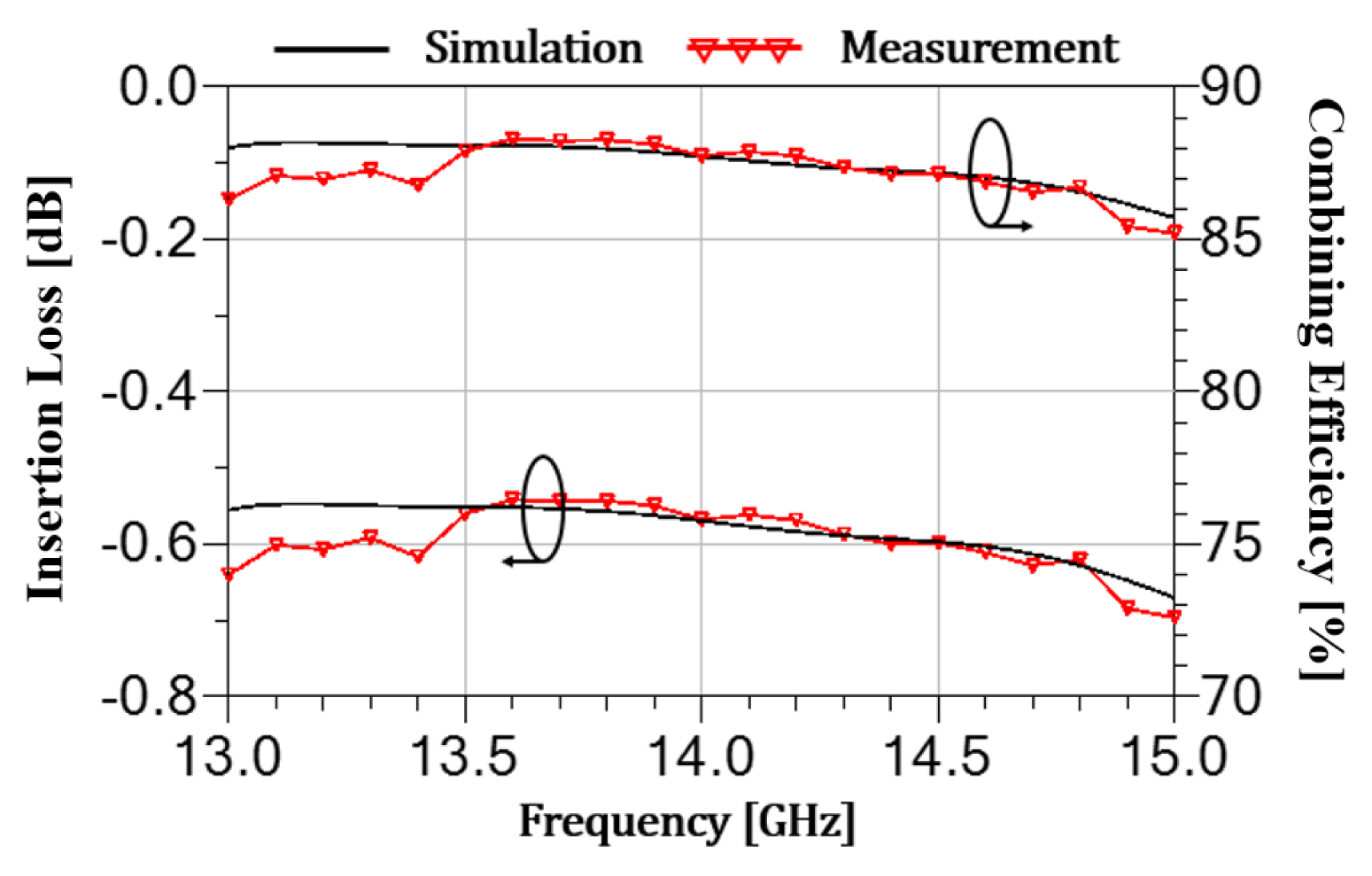
Fig. 13 compares the simulated and measured insertion loss and power combining efficiency of the HSIW-based 1:3 traveling-wave power divider. The power divider had a measured insertion loss of 0.57 ± 0.03 dB and a measured power combining efficiency of 87.1%–88.3% from 13.5 GHz to 14.5 GHz, consistent with the simulated results.
We compared our measured results with those of previously published power dividers in Table 5 [10, 11]. Compared with the results in literature [10] that used waveguide-type components, the insertion loss of our 1:3 power divider increased by 0.2 dB, and the power combining efficiency decreased by 3%. As it used only one transition, [10] seemed to have a similar performance to our work if one transition loss was added, but it had a wider frequency performance. The comparison of our work with the corporate power divider in [11] also showed that our work improved the insertion loss by 1.4 dB and the power combining efficiency by 24%.
Our HSIW-based power divider has the advantages of low cost and mass production due to the simple PCB process. Therefore, it is promising for applications requiring both high performance and competitive cost.
V. Conclusions
A microstrip-to-HSIW transition using C-cut via holes and an HSIW-based 1:3 traveling-wave power divider employing the proposed transitions were demonstrated for Ku-band applications. The fabricated back-to-back transition showed a return loss of 18 dB or more and an insertion loss of 0.5 dB from 12.5 GHz to 15.5 GHz. The power divider using the transitions had a return loss of more than 21 dB, an insertion loss of 0.57 dB, and a power combining efficiency of 87.1% or more from 13.5 GHz to 14.5 GHz. The developed traveling-wave power divider using the HSIW structure can be effectively used in Ku-band applications that require low loss and small size in addition to high performance.