I. Introduction
Microstrip patch antennas have been widely employed in wireless communication systems, mainly owing to their low cost, low profile, and easy fabrication. However, patch antennas usually have the disadvantage of a narrow bandwidth.
A proximity-coupled microstrip patch antenna has broadband characteristics compared to the probe-fed and edge-fed coupling methods. In the proximity-coupled microstrip configuration, the bandwidth can be increased by 10%–26% using a stacked radiator, L-probe feeding, and slot patch using stubs [1–4].
Placing the cavity-backed ground under the patch improves the bandwidth by reducing the surface wave and lowering the equivalent dielectric constant. Many microstrip antennas have been designed and studied on cavity structures to increase bandwidth [5–12]. In [6], a stacked patch with a cavity-backed ground plane enhanced the impedance matching and improved the bandwidth to 26%. In [11], a narrow cavity was used to create an efficient coupling of patches with thick substrates, and the bandwidth was increased to 40% by increasing the coupling amount.
In [12], a cavity-backed patch antenna with proximity coupling fed using a conventional microstrip feed line is presented that achieves 69.6% voltage standing wave ratio (VSWR) bandwidth. There are three substrate layers and its height corresponds to 0.38λ0, where λ0 denotes the wavelength of the operational center frequency.
In this paper, we propose a broadband cavity-backed proximity-coupled patch antenna on two substrate layers modified with a rectangular open-ended microstrip feed line (OEMF). The rectangular OEMF is defined as the combination of a rectangular patch and microstrip feed line. The rectangular OEMF technique can maintain the bandwidth and generate additional resonances to create a bandwidth expansion effect compared to those of conventional microstrip feed line. The proximity-coupled patch and rectangular OEMF are placed on upper and lower substrates on a cavity structure to generate multiple resonances in different frequency bands. The rectangular OEMF on the lower layer is designed to achieve an upper band VSWR bandwidth through the coupling with the cavity. The upper layer patch fed by the rectangular OEMF with the cavity realizes the lower band VSWR bandwidth. As a result, the proposed antenna realizes 77% VSWR bandwidth from 5.6 GHz to 12.6 GHz with the dimensions of 0.9λ0 × 0.9λ0 × 0.27λ0 (width × length × height), where λ0 corresponds to the free space wavelength of 9 GHz.
II. Antenna Design
The geometry and parameters of the antenna are shown in Fig. 1. The antenna consists of a patch, substrate 1 and 2, a rectangular OEMF, and a cavity-backed structure.
The dimensions of the patch are W2x × L2y and it is placed on the substrate 2 at height h2. The antenna is fed through proximity coupling between the patch and the rectangular OEMF. The rectangular OEMF has a size of W1x × L1y, and the length of the feed line is Ly. The length between the cavity starting point and ground end on the y axis is Lc. A ground plane with a cavity is placed below substrate 1. The antenna parameters were ɛr1 = ɛr2 = 2.2, W2x = 13.72 mm, L2y = 7.25 mm, h1 = 0.508 mm, h2 = 3.175 mm, W1x = 7 mm, L1y = 6.25 mm, Ly = 9 mm, Lc = 9 mm, Wcx = 11.65 mm, Lcy = 26.58 mm, and Hcz = 3.74 mm.
Variations of the design parameters of the cavity, patch and rectangular OEMF affect the input impedance and resonant frequency of the antenna. In the following parameter study, only a rectangular OEMF and the parameter of focus are varied, and the remaining parameters are maintained as presented above.
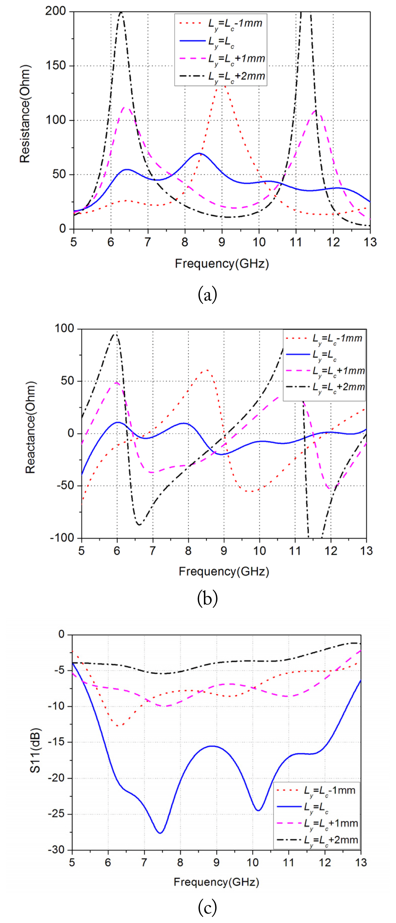
Fig. 2 shows the variation of input impedance and reflection coefficient when the length of the rectangular OEMF(Ly) is changed. In case of Ly > Lc, upper and lower resonances occur, but the impedance between the two resonances is not matched to 50 Ω. In the case of Ly = Lc, the impedance is roughly 50 Ω and the impedance variation is small, which means that broadband matching occurs. In the case of Ly < Lc, a single resonance occurs near 9 GHz, and the resistance in the other frequencies is smaller than 50 Ω and the variation of the reactance increases. Consequently, the broadband matching is broken. S11 also has the largest bandwidth when Ly = Lc.
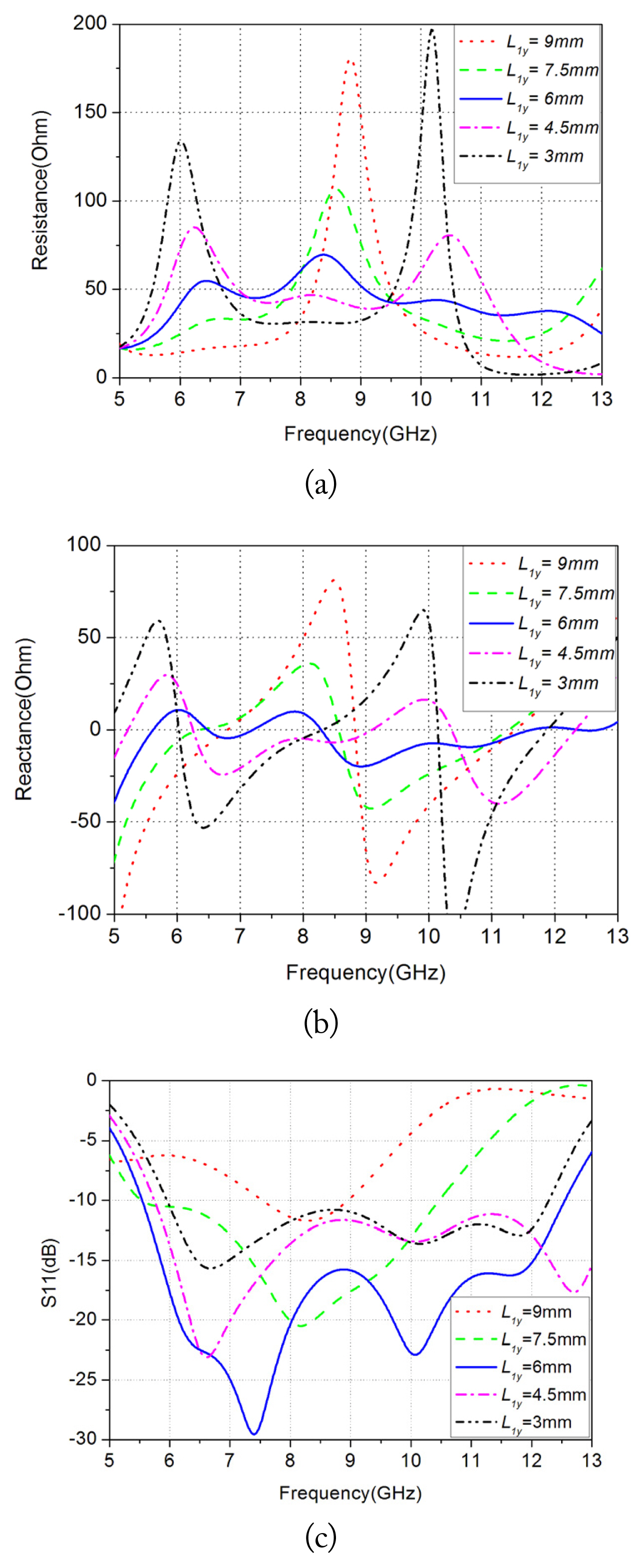
Variations of input impedance when all parameters are the same and only L1y is changed, meaning the length of the y-direction of the rectangular OEMF when the end of the rectangular OEMF is aligned with the center of the top patch, are shown in Fig. 3. It can be seen that when L1y is 6 mm, S11 has the widest bandwidth characteristic. When L1y is larger than 6 mm, a single resonance occurs. As L1y becomes smaller, the resonance peak decreases. It can be seen that broadband matching occurs when the end of the cavity and the starting point of the rectangular open ended microstrip coincide on the y-axis (L1y = 6 mm).
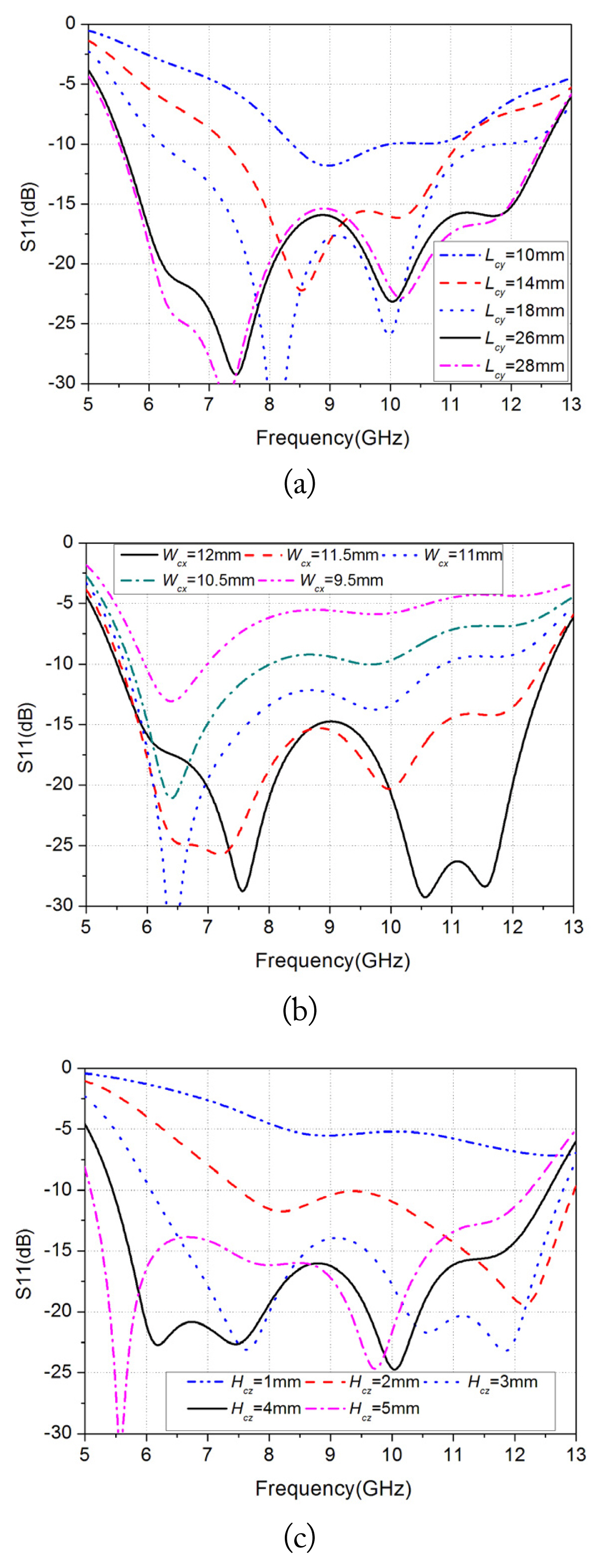
Fig. 4 shows the change in reflection coefficients when the dimension of the cavity is varied. As Lcy became larger, broadband matching occurred. Wcx showed a bandwidth increase when it was increased to 12 mm. Hcz exhibited good bandwidth at about 4 mm and when Hcz was too low, bandwidth was significantly reduced. It can be seen in Fig. 4 that additional resonance in the upper frequency band occurs, especially when the cavity is large (Lcy ≥ 26 mm, Wcx ≥ 11.5 mm, Hcz ≥ 3 mm).
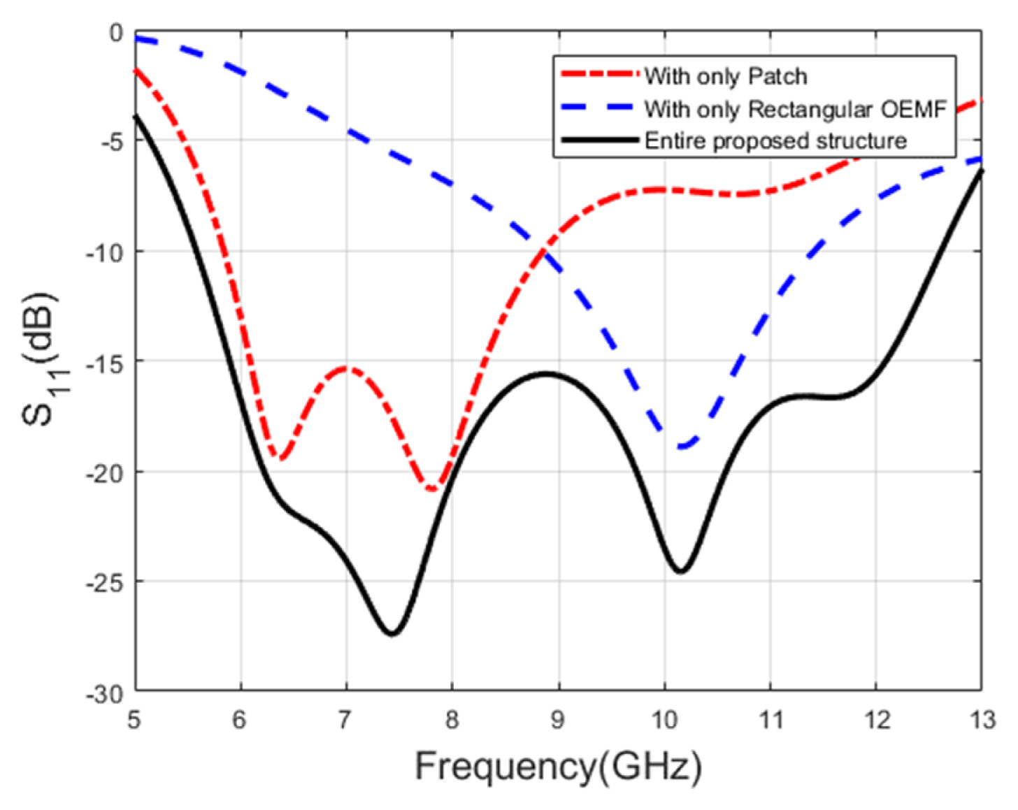
Fig. 5 shows results of S11 for the structure with only the patch, only the rectangular OEMF, and the whole proposed structure. The antenna with only the patch is for the structure where only the narrow feed line is extended with the same length. Only the rectangular OEMF is for the structure without the patch and the substrate 2. The S11 characteristic of the structure with only the patch (W1x = 1.8 mm) has a bandwidth of approximately 26% in the low band of 6 to 9 GHz, which shows the bandwidth performance when the cavity is coupled to the proximity-coupled antenna. The S11 characteristic of the structure with only the rectangular OEMF (W2x = 0 mm) has a bandwidth of approximately 20% in the high band of 9 to 12 GHz, which shows the bandwidth expansion effect of the rectangular OEMF on the entire structure. The rectangular OEMF allows additional bandwidth to be secured while maintaining the existing bandwidth. The S11 characteristics of the proposed structure are shown by combining the characteristics of the structure with only the patch and the structure with only the rectangular OEMF. Because the proximity-coupled microstrip antenna with cavity-acked structure mainly operates at the lower band and the added rectangular OEMF as a modified feed line mainly operates at the upper band, the combination of the two structures eventually increases the bandwidth.
It can be seen that a bandwidth of approximately 77% is realized from 5.6 to 12.6 GHz. It can be observed that VSWR bandwidth is almost doubled compared with the conventional method [12]. All the simulations were performed using the commercial software Computer Simulation Technology (CST) Microwave Studio.
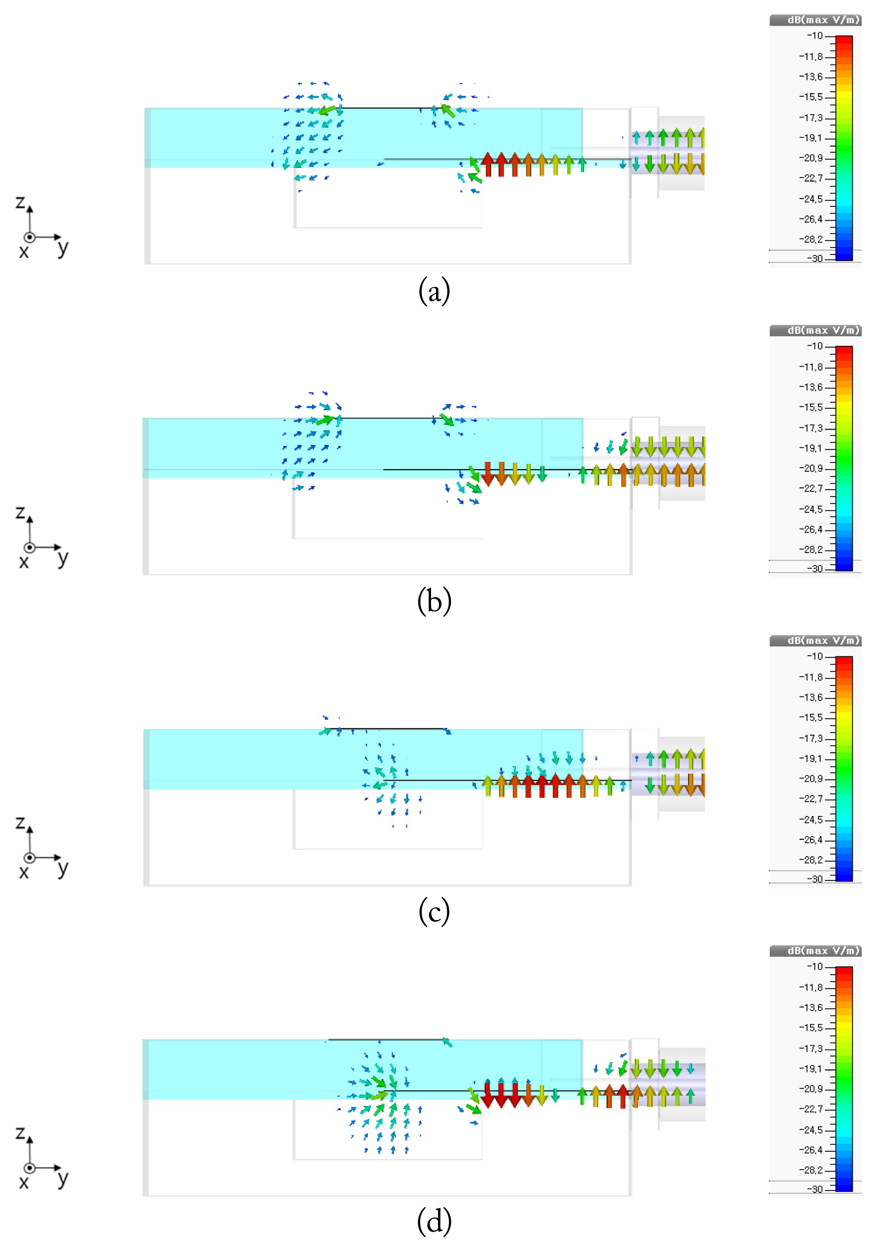
Electric field distributions on the y-z plane show the status of the resonance of patch and rectangular OEMF depending on the frequency variation. The simulated field distributions for the three frequencies in the side view are shown in Fig. 6. In the case of 6.4 GHz and 7.4 GHz, it can be seen that resonance mainly occurs in the patch. In the case of 10.1 GHz and 11.8 GHz, it can be seen that resonance occurs mainly in the rectangular OEMF, and very weak resonance occurs in the patch.
III. Fabrication and Measurement Results
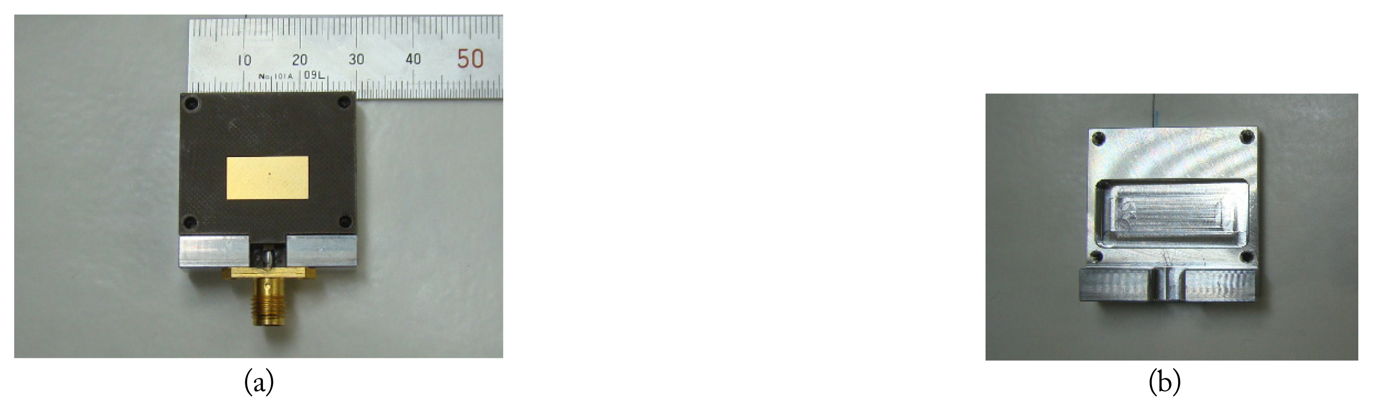
An antenna prototype was fabricated as shown in Fig. 7. To connect a coaxial connector, additional housing with aluminum was added to the side of the antenna, which only negligibly affects the antenna performance.
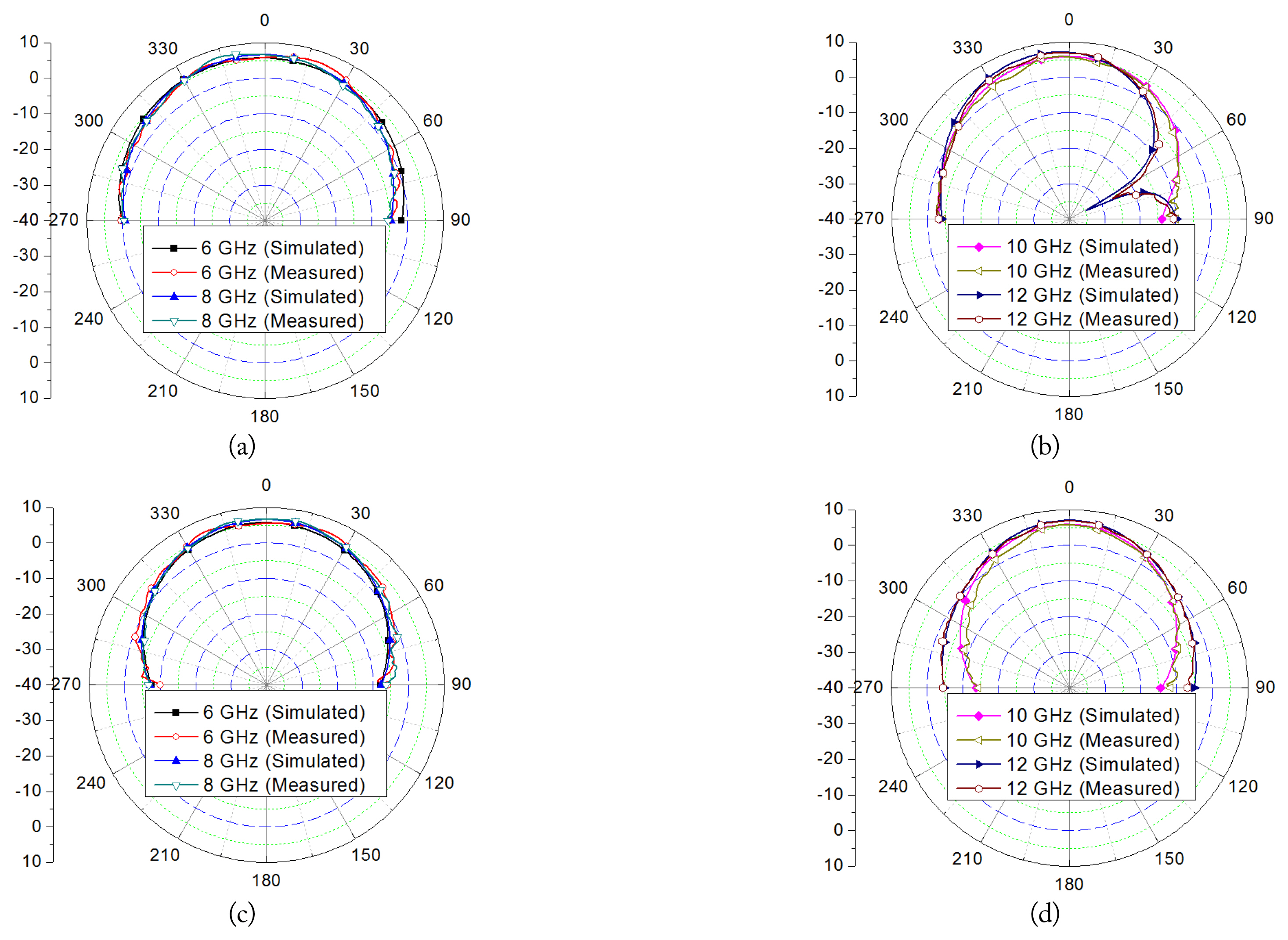
The simulation and measurement results of the co-polarization patterns at 6, 8, 10, and 12 GHz for E-plane and H-plane are presented in Fig. 8. The measured results were found to be consistent with the simulated ones. The asymmetry of the E-plane radiation pattern gradually tends to increase with the increase in frequency.
At 12 GHz, a null is generated in approximately 60° direction, which causes a narrowing of the antenna beam width. The radiation pattern was found to be distorted due to the physical asymmetry of the antenna on the z-y plane.
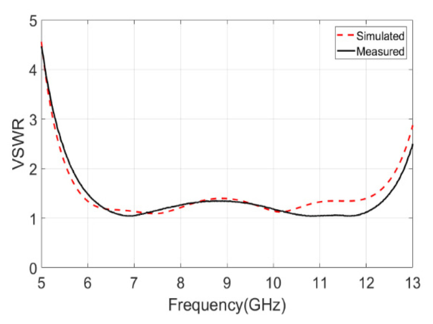
As shown in Fig. 9, the VSWR was simulated and measured. The VSWR bandwidth was measured to be more than 77% for the proposed antenna. The measured result was consistent with the simulated one.
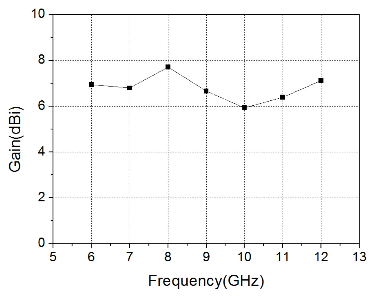
Fig. 10 shows the measured gains of the proposed antenna. A reasonably good radiation gain from 6 dBi to 8 dBi is obtained within the entire operating band.
IV. Conclusion
This paper proposed a broadband modified cavity-backed proximity-coupled microstrip patch. The patch was designed to resonate with the cavity in the lower band and the rectangular OEMF to resonate with the cavity in the upper band, resulting in a bandwidth as high as 77% (VSWR ≤ 2.0) across a frequency range of 5.6 to 12.6 GHz. The proposed antenna configuration with a cavity-backed ground plane is easy to fabricate and is expected to be applicable to wideband array antennas.