Uncertainty of S-Parameter Measurements on PCBs due to Imperfections in the TRL Line Standard
Article information
Abstract
This paper evaluates the uncertainty of S-parameter measurements on multilayer printed circuit boards (PCBs) due to the uncertainties of the dimensions and dielectric properties of the line standard in the Thru-Reflect-Line (TRL) calibration. This evaluation is performed in two ways: one is based on repeated TRL calibrations with a randomly perturbed line standard, and the other is based on equations given by Stumper. The two methods require the uncertainties of the S-parameters of the TRL line standard, which are obtained from the uncertainties of the dimensions and dielectric properties using three-dimensional electromagnetic Monte Carlo simulation. The two methods agree well with each other. This study also shows how to apply impedance renormalization in Stumper’s equations. We design the TRL standards and the devices under test (DUTs) in PCB stripline and precisely measure the cross-sectional dimensions of the fabricated striplines. Uncertainty analysis based on the measured values enables us to investigate the impact of realistic deviations in the dimensions of the TRL line standard on the S-parameter measurement uncertainty of the DUTs. Finally, as an example, we evaluated the uncertainty in the measured S-parameters of a Beatty line on the fabricated PCB.
I. Introduction
Due to the high level of integration that can be achieved and the ease of design, circuits implemented on printed circuit boards (PCBs) are widely used. In addition, the development of new materials and processes has enabled PCB designs at higher frequencies. Accordingly, de-embedding techniques have been studied to accurately evaluate circuits (or devices) on planar substrates. Among them, techniques using calibration methods, such as Thru-Reflect-Line (TRL) and Line-Reflect-Line (LRL) have enabled accurate measurements, even at high frequencies [1].
Accuracy of the de-embedding method based on TRL calibration is largely dependent on the uncertainty of the characteristic impedance of the TRL line standard [2]. This uncertainty is determined by evaluating the uncertainties in the cross-sectional dimensions and the dielectric properties (permittivity ɛr and loss tangent tanδ) of the line standard. Because PCB manufacturing exhibits high tolerance and an accurate evaluation of the dielectric properties of the materials used to fabricate a multilayer PCB is challenging, the derived characteristic impedance has significant uncertainty.
This uncertainty in the TRL line characteristic impedance results in uncertainty in the measured S-parameters of a device under test (DUT). This is because the S-parameters of a DUT measured with respect to TRL calibration are referenced to the actual characteristic impedance of TRL line, Zline, which, in general, is not exactly 50 Ω. Therefore, the S-parameters of the DUT are often required to be referenced to an idealized reference impedance, Zref (which is often 50 Ω), and so the S-parameters are renormalized from Zline to Zref [3, 4].
Several methods are available for determining the characteristic impedance. One of the well-established methods is the method in which the characteristic impedance is derived from the propagation constant and estimated capacitance per unit length of the line [5, 6]. Another well-established method is the calibration comparison technique [7, 8]. The former method assumes that the substrate has low loss; thus this technique is neither applicable to lossy substrates nor at very high frequencies. In the latter method, the characteristic impedance is calculated from the error boxes obtained by two-tier calibration when the reference impedance of the first calibration is known. This approach has the advantage of being less impacted by the effects of probe pads. However, if the transition from these pads to the line is inductive, the calibration comparison technique requires additional correction [8]. In this case, there remains a question concerning how to evaluate the value of inductance. Therefore, this method is less reliable for lines with long transitions.
A recent study [9] introduced a new method based on three-dimensional (3D) electromagnetic (EM) simulation. This method can provide comparable accuracy to the calibration comparison method. The uncertainty in the TRL line characteristic impedance and its impact on the measured DUT S-parameters was demonstrated by employing the method described in [10]. The impact was shown as the worst-case deviation from the reference simulated S-parameters.
In this study, we evaluate the uncertainty in the measured DUT S-parameters due to the uncertainty in the dimensions and dielectric properties of the TRL calibration line standard using two extraction methods: (i) a method based on repeated TRL calibrations with a randomly perturbed line standard and (ii) a method combining impedance renormalization using the equations given by Stumper [11]. Both methods employ 3D EM Monte Carlo simulation provided by the Advanced Design System (ADS) circuit simulator [12] to obtain the uncertainties in the characteristic impedance and S-parameters of the TRL line standard. This study shows how to combine impedance renormalization with Stumper’s equations. Using these methods, we evaluate the uncertainty in the measured S-parameters of the DUT fabricated on the multilayer PCB.
The rest of this paper is organized as follows. In Section II, we present the nominal values of the line dimensions and dielectric properties and the associated uncertainties; we also discuss how to evaluate the uncertainty in the dimensions of the fabricated PCB line. In Section III, we introduce the two methods for evaluating the uncertainty in the measured DUT S-parameters based on 3D EM Monte Carlo simulation. The simulation results are presented in Section IV. The S-parameters of the DUT, measured using a vector network analyzer (VNA), and the evaluation of the uncertainty in these measured S-parameters, are presented in Section V.
II. Sources of Uncertainty
The calibration standards and DUT are realized in stripline on the PCB. The cross-sectional structure of the fabricated PCB is shown in Fig. 1. It consists of four dielectric layers and three metal layers. The strip line is connected to the coplanar waveguide (CPW) line on the top layer through at each end. To maintain the same ground on the upper and bottom planes of the stripline, we connected two planes through the vias, which is distributed along the line at the fixed intervals. In this paper, it is assumed that the effect of the ground vias on the characteristic impedance is small and, thus, we ignore the effect. The top view and cross section (at “A” in Fig. 1) of the stripline are presented in Fig. 2(a) and 2(b), respectively. The dielectric materials constituting the substrate are RO4350 (D1) and prepreg 2116 (D2). The prepreg material is essential when fabricating multi-layer PCBs.
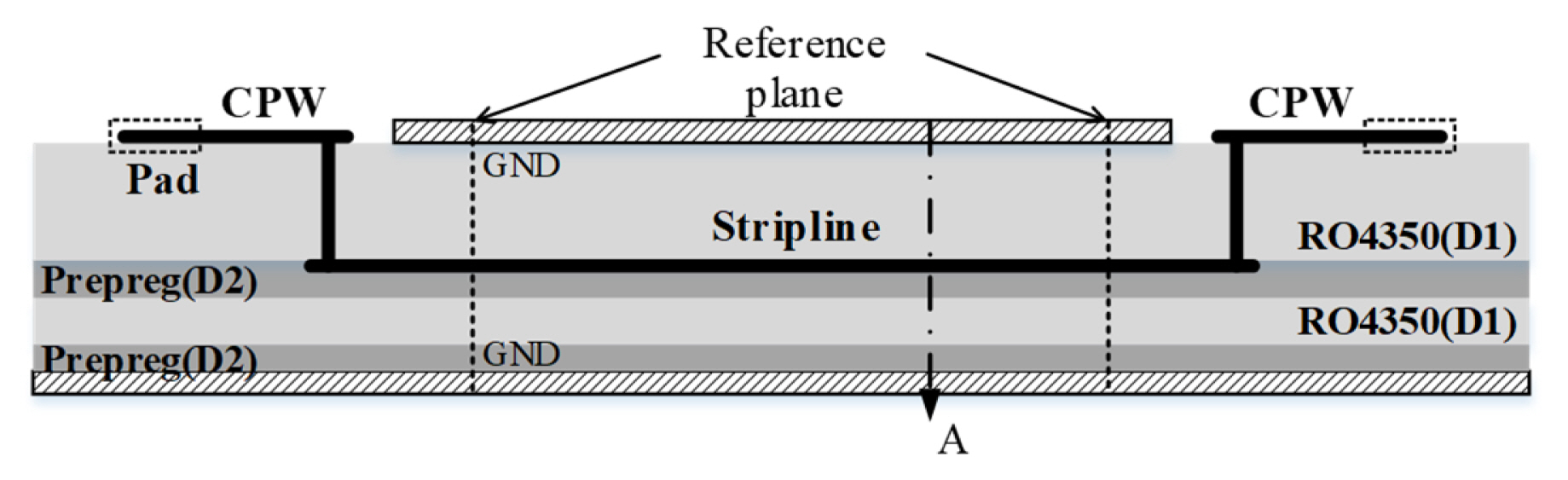
Configuration of the implemented stripline.

Fabricated PCB: (a) top view and (b) cross-section.
The characteristic impedance of the stripline is determined from the width of the line (WSL), its thickness (TSL), thicknesses of the dielectric material (H1, H2), and the dielectric properties (ɛr, tanδ); the uncertainties in all these quantities propagate to the uncertainty in the characteristic impedance and the uncertainty in the S-parameters of the DUT, subsequently.
The dimensions of the fabricated striplines are measured by taking a micro-section of the PCB and performing dimensional measurements with a high-resolution vision measuring machine of resolution 0.1 μm. When measuring WSL, we corrected the values by measuring the angle between the cut plane and the plane perpendicular to the striplines. All 26 lines on the PCB are measured, and the mean and standard deviation of the measured values were calculated. This information is summarized in Table 1 [13–15]. Using the mean values of the measured dimensions, an average value for the characteristic impedance (

Dimensions of fabricated stripline (unit: mm)
We cut the PCB using an endmill, which is a type of milling cutter. During the cutting procedure, line deformation can occur at the cross-section. This deformation may cause the mean of the measured dimensions to somewhat deviate from the actual value, and the standard deviation in the measured dimensional values to increase. Nonetheless, we use the measured values to determine the impact on the derived characteristic impedance.
In the case of permittivity and the loss tangent, we refer to the datasheet for RO4350 and a report written by the prepreg manufacturer [16]. However, the uncertainty is given only for D1 permittivity. Therefore, in the absence of any other information, we assume that the uncertainty of D2 permittivity is the same as that of D1, and the uncertainty in the loss tangent is ±10%, in order to investigate these effects. The permittivity and loss tangent of the dielectric materials are summarized in Table 2. These properties depend on the PCB structure, and the properties for the prepreg also depend on the composition (e.g., the amount of water and resin present in the prepreg) [16]. For an accurate evaluation of these quantities, it is necessary to understand the measurement method used to determine the dielectric properties.
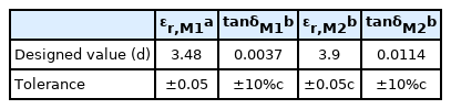
Property of dielectric materials (D1, D2)
Using the values listed in Table 3, we perform Monte Carlo simulations. Gaussian distributions were assigned to each TRL line parameter (WSL, TSL, H1, H2, ɛr,M1, ɛr,M2, tanδM1, and tanδM2). H2 contains three layers of material, which are varied proportionally during the simulations, for simplicity. The number of Monte Carlo trials is selected as 1,000 for each simulation, which results in a computation time of approximately 10 hours.

Variables for Monte Carlo simulation
III. 3D EM Monte Carlo Simulation
We use the momentum simulator provided by ADS for the 3D EM Monte Carlo simulation. We model the stripline for the TRL calibration line standard of length 1.2 mm between the reference planes shown in Fig. 1. The dimensions of the horizontal and vertical structures of the line and the dielectric properties are parameterized, and Monte Carlo simulations are conducted for these variables. The feed type for the ports is TML, which stands for the transmission line calibration. The TML ports de-embed the feed structures.
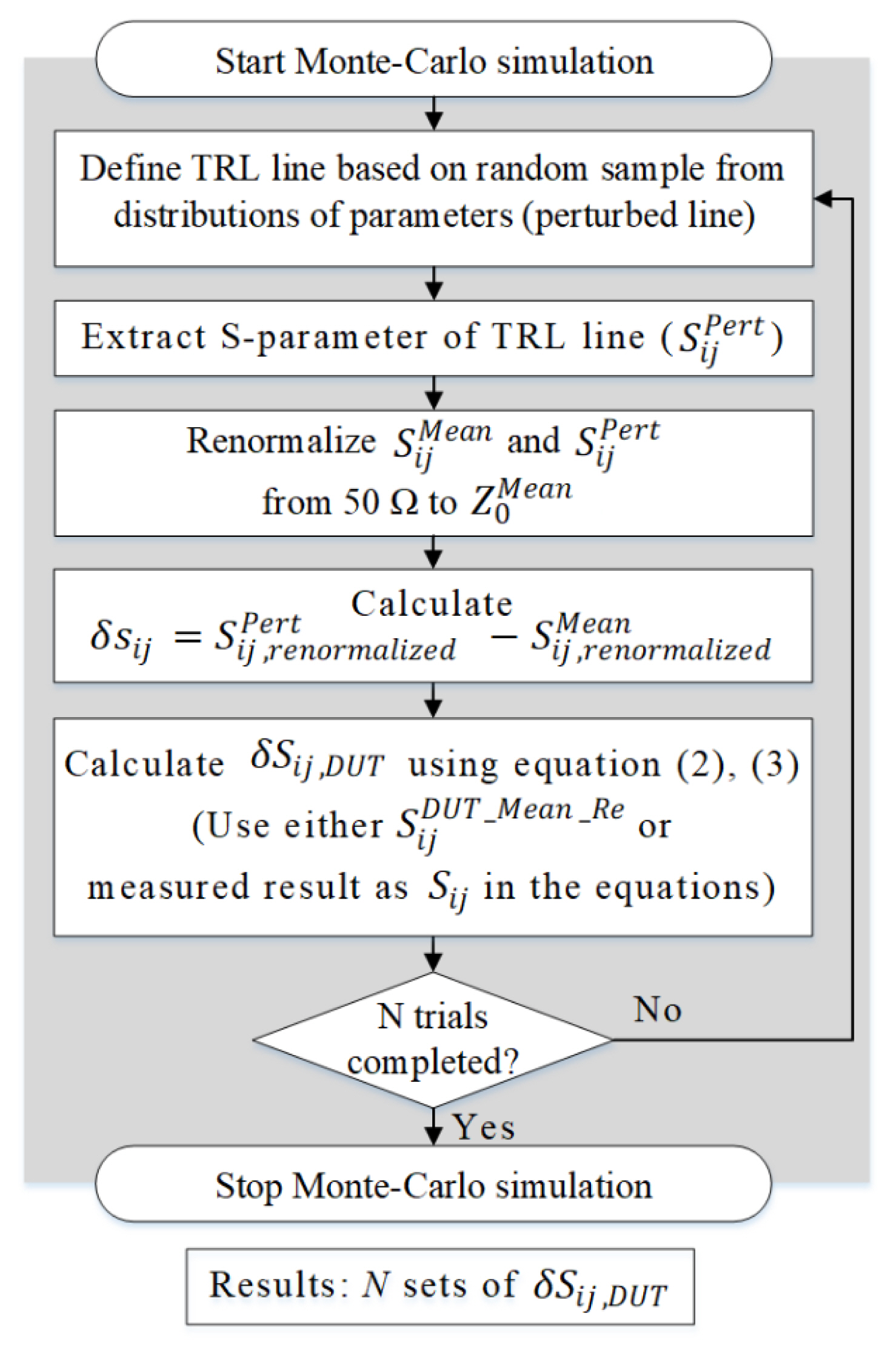
We use two methods for the 3D EM Monte Carlo simulation, which are based on (i) repeated TRL calibration and (ii) Stumper’s equations. The former method repeats TRL calibration using lines with randomly perturbed dimensions and dielectric properties. The DUT S-parameters are then renormalized from an assumed initial reference impedance of
where the S-parameters are the simulated values for TRL line and Zsys is the system reference impedance of the simulator, which is generally 50 Ω. This equation is applicable only to uniform lines.
The latter method repeatedly calculates the deviation of the DUT S-parameters (δSij,DUT) using the deviation of the S-parameters of TRL line (δsij) obtained by randomly varying the dimensions and dielectric properties, as well as the Stumper’s equations shown below [11]:
where L = exp (−γl), l is the TRL line length and γ is its propagation constant obtained as a by-product during the TRL calibration process, Γrefl is the reflection coefficient of the TRL reflect standard, and Sij are the DUT S-parameters. To obtain corresponding expressions for δS22,DUT and δS21,DUT, index 1 is replaced by 2 and vice versa in Eqs. (2) and (3).
As seen from the above equations, the S-parameter uncertainty increases as the length of the line standard approaches n times λ/2, where n is an integer. In this study, a single line is used as the Monte Carlo simulation takes a long time. To obtain a lower uncertainty at low frequencies, more lines with longer length can be used.
The process used for both methods is shown in Fig. 3. First, we define the “mean” line using the mean parameter values. We extract the S-parameters and Z0 of this “mean” line, which are assigned as

Flow chart for the process common to the two methods for extracting the uncertainty of the DUT S-parameters.
In this study, we use a Beatty line as the DUT, as shown in Fig. 4. It consists of a center line, with a width of 2 mm and length of 30 mm, and outer lines, with a width of 0.6 mm and length of 5.2 mm, at both ends of the center line. We assume that all fixtures, which consist of a transition from CPW to stripline, are identical. The fixtures, which are included in the ADS simulation, constitute the error boxes for TRL calibration.

Diagram of the Beatty line.
1. Method based on Repeated TRL Calibration
Fig. 5 shows a flowchart for the Monte Carlo simulation based on repeated TRL calibration. We define TRL line again using the perturbed parameters (i.e., “perturbed line”). Then, we calibrate using the perturbed line and correct the DUT S-parameters. Finally, we renormalize the DUT S-parameters to 50 Ω assuming that they are initially normalized to

Flow chart for Monte Carlo simulation based on impedance renormalization.
2. Method based on Stumper’s Equations
Fig. 6 shows a flowchart for the Monte Carlo simulation based on Stumper’s equations. TRL line is defined again with the perturbed parameters (perturbed line), and then the S-parameters are extracted for the perturbed line (
Flow chart for Monte Carlo simulation based on equations given by Stumper.
IV. Simulation Results
From the method based on Stumper’s equations, we have S-parameters (
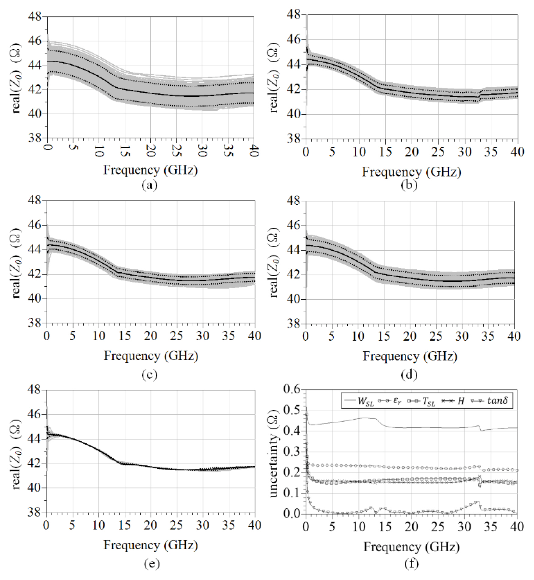
The simulation results of real part of Z0 for each parameter of (a) WSL, (b) TSL, (c) H1,H2, (d) ɛr, and (e) tanδ. The black line indicates
In Fig. 7(f), we plot all these uncertainties, obtained from the standard deviations, which show that the uncertainty with respect to WSL is dominant for the conditions listed in Table 3. This shows that, to evaluate the characteristic impedance with low uncertainty, high accuracy is required when measuring the line width.
To account for the case in which the measurement of the line width is affected by the cutting process of the endmill, resulting in large uncertainties, we also measure the width of the CPW lines on top of the same PCB. The standard deviation of the measured CPW line width is 0.006 mm, which is approximately half that of the striplines. It is difficult to say if this value can be used as the uncertainty for the stripline measurement because the fabrication process for the stripline is different from that for the CPW line. Even if we do use this value, we obtain an uncertainty of 0.25 Ω at 20 GHz, which is still a dominant contribution to the overall uncertainty.
In the simulated results shown in Fig. 7, small resonances are observed at specific frequencies (e.g., at 33 GHz). We perform simulations using lines of different lengths, but the resonances always occur at the same frequencies. This is presumed to be a resonance phenomenon of the multilayer structure itself.
By the repeated TRL process, we obtain 1,000 sets of S-parameters for the DUT (Beatty line), as shown in Fig. 8. Fig. 8 and 8(b) shows the magnitude of S11 and S12, according to the deviation of WSL, respectively. The black line indicates the result obtained from the mean values of the parameters and the gray lines indicate those obtained from the perturbed values. Finally, the uncertainty caused by TRL line can be obtained by calculating the standard deviation of the 1,000 S-parameter results at each frequency. The uncertainties of |S11| and |S12| are presented in Fig. 9.
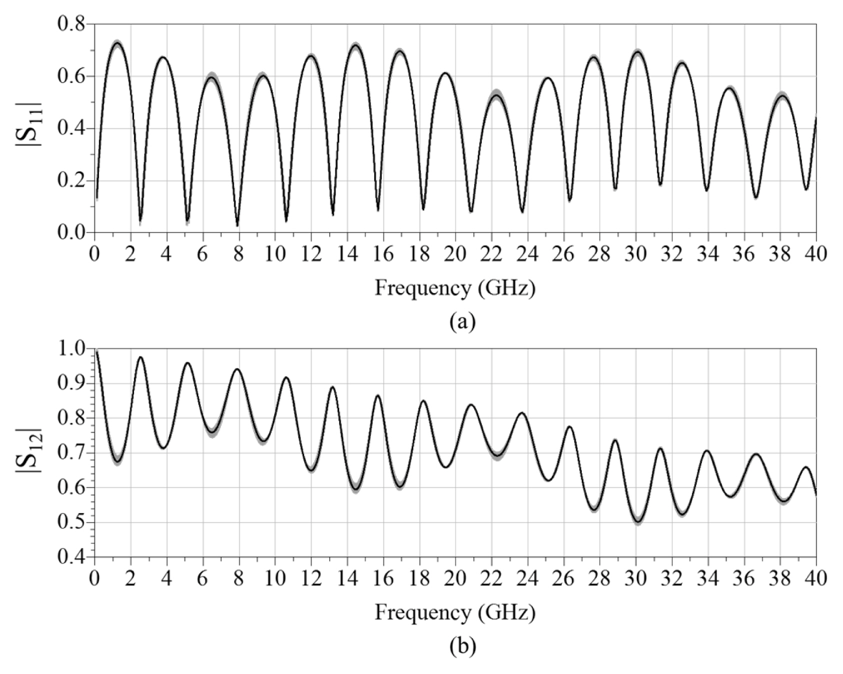
Monte Carlo simulation results of magnitude of the DUT S-parameters (a) S11 and (b) S12 with respect to the parameter WSL, using the method based on repeated TRL calibration.

Comparison of the results obtained from the two methods. Magnitude uncertainty of the DUT S-parameters (a) S11 and (b) S12 with respect to the parameter, WSL.
Fig. 9 also plots the results based on Stumper’s equations. In this simulation, we use the simulated values for the DUT S-parameters Sij. Both sets of results agree exactly with each other. If we do not renormalize the S-parameters of TRL line from 50 Ω to Z0, there is a discrepancy between the two methods.
When performing the uncertainty analysis, it is important to consider what factors influence the uncertainty. By using Stumper’s equations, it is easier to identify the influences and interactions that affect the uncertainty in the measurement results. For example, by calculating the sensitivity coefficients for δs11 and δs12, we can verify how each uncertainty contribution affects the uncertainty in the DUT S-parameters. The sensitivity coefficient of δs11 for u(|S12|) is S22·S12/(1−L2), from Eq. (3), which is plotted in Fig. 10(a). By multiplying the sensitivity coefficient by the uncertainty of δs11, we obtain the uncertainty contribution for δs11. Fig. 10(b) shows the uncertainty of δs11, obtained by the Monte Carlo simulation, and Fig. 10(c) shows the uncertainty contribution for u(|S12|).
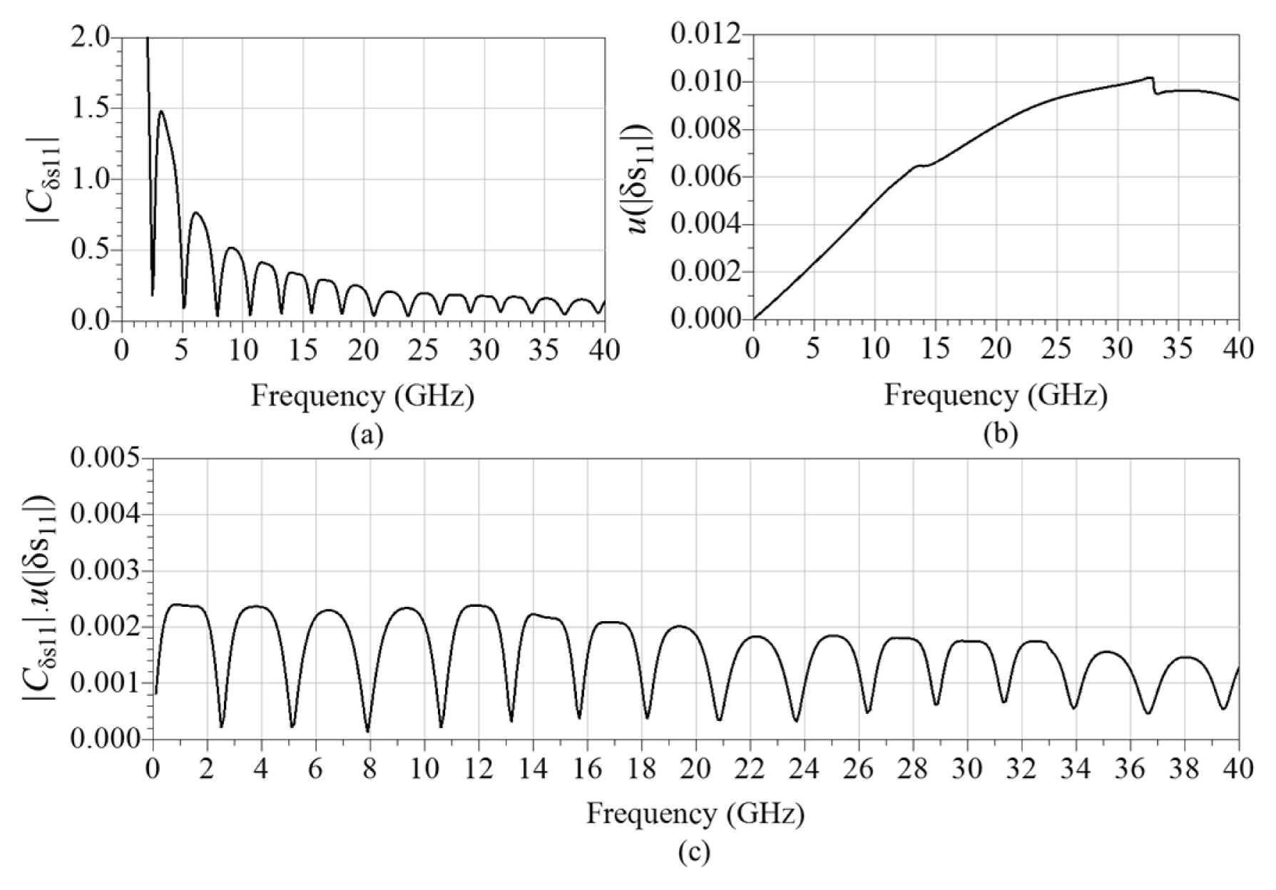
(a) Sensitivity coefficient of δs11, |Cδs11|, for u(|S12|) from the Stumper’s equation, (b) uncertainty of δs11 and (c) its uncertainty contribution to u(|S12|).
Fig. 11 presents the uncertainty contributions for each DUT S-parameter. As expected from the results of characteristic impedance, the uncertainty caused by the width of the line, WSL, is the dominant contribution.
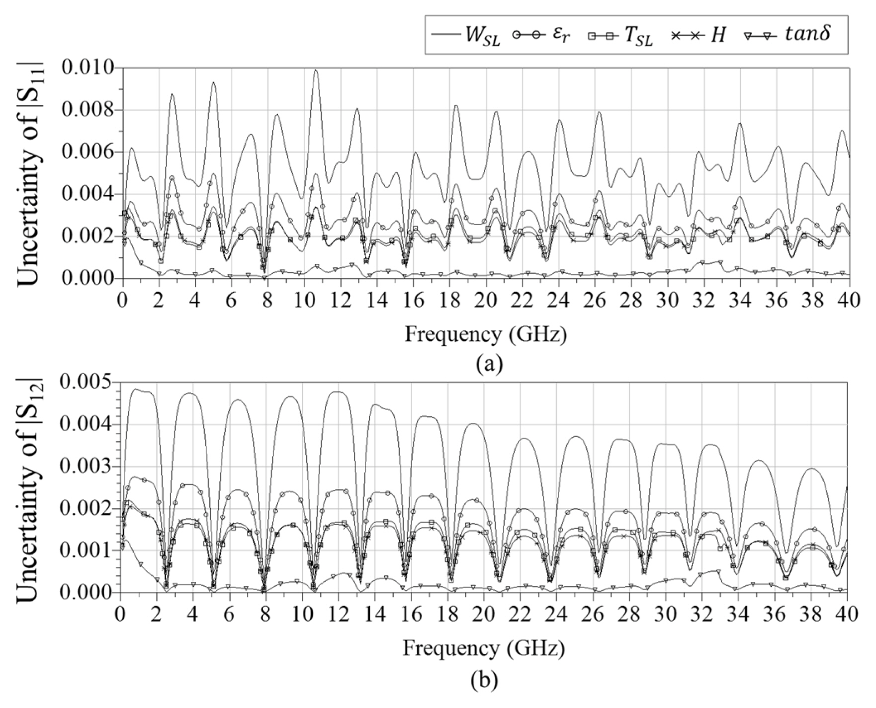
Standard uncertainty of (a) |S11| and (b) |S12| due to the uncertainties in WSL, TSL, H, ɛr, and tanδ.
V. Experimental Results
The measured and simulated S-parameters of the DUT (Beatty line) are shown in Fig. 12(a) and 12(b), respectively. The solid line shows the measured results, and the dotted line shows the simulated results. Because the datasheet for RO4350 does not provide the frequency dependency of permittivity in this specific multilayer structure, this simulation does not consider any change in the values of the permittivity and loss tangent with regard to frequency. This is likely to cause a slight discrepancy between the simulated and measured results shown in Fig. 12(a) and 12(b).
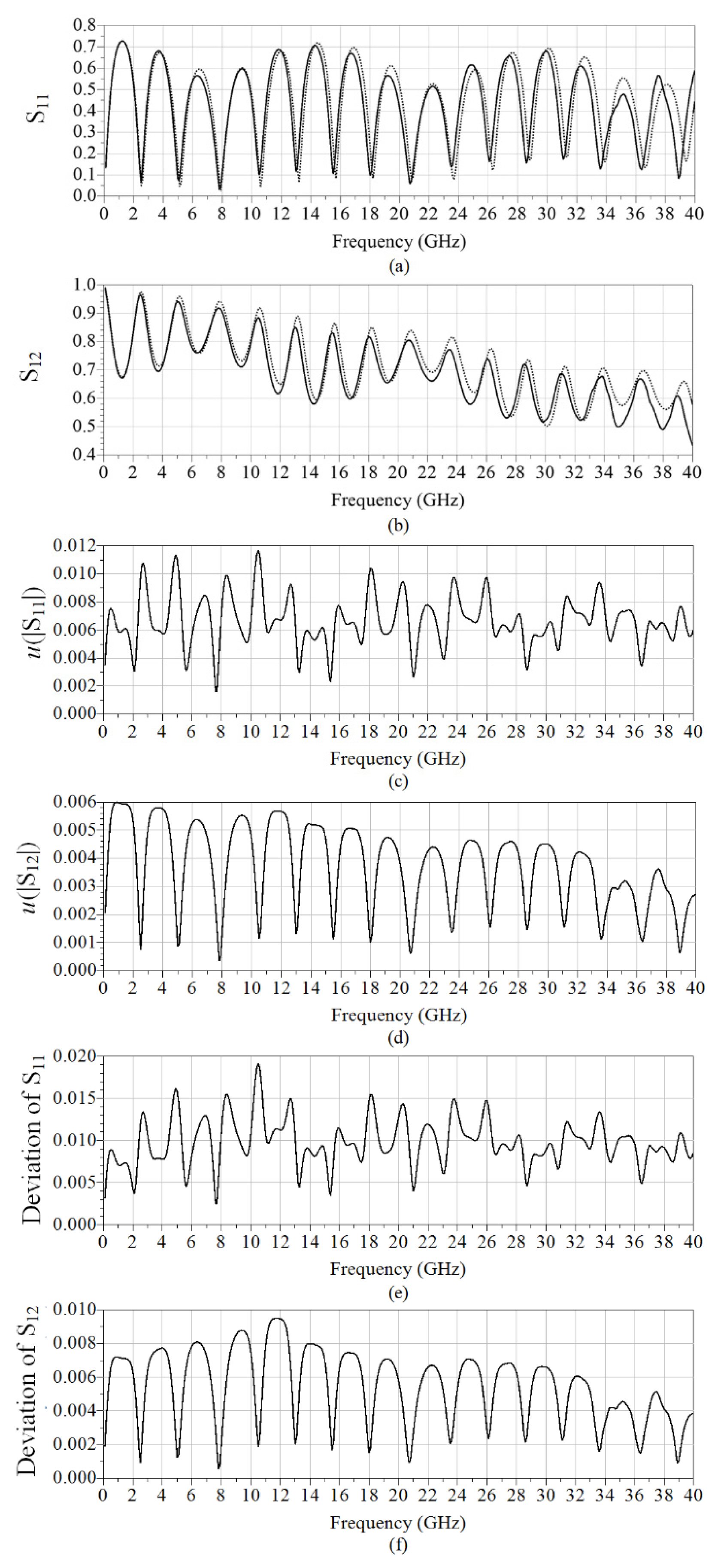
Measured (solid) and simulated (dotted) (a) |S11| and (b) |S12| of DUT, and (c, d) their uncertainty for all sources of uncertainty obtained by 3D EM Monte Carlo simulation (N = 1,000). Deviation of DUT S-parameters (e) |S11| and (f) |S12| from the results obtained using TRL line width designed values.
We use a two-tier calibration to perform the measurements. The first-tier calibration is a short-open-load-thru (SOLT) calibration at the ground-signal-ground (GSG) probe tips made using a commercial impedance standard substrate. The secondtier calibration is a TRL calibration performed using calibration standards on the PCB to move the measurement reference planes to the stripline terminals of the DUT. In this study, we do not consider the uncertainty caused by first-tier calibration.
To calculate the uncertainty, we select the method based on Stumper’s equations, which enables us to use the measured values of DUT S-parameters. First, we obtain the uncertainty of the line, δsij, using the 3D EM Monte Carlo simulation with 1,000 trials, as discussed in Section III. The uncertainties of |S11| and |S12|, with respect to all parameters, are obtained from the measured DUT S-parameters and δsijs. These uncertainties are presented (as standard uncertainties) in Fig. 12(c) and 12(d). Their null positions are matched with those of the measured S-parameters.
Fig. 12(e) and 12(f) shows the deviation of the measured S-parameters of the DUT (obtained using the measured mean values) from the values obtained assuming the designed (i.e., intended) values listed in Table 1. We use the measured DUT S-parameters. The deviations are generally larger than the uncertainty, which indicates the need to use the measured values for each fabricated PCB, rather than the designed (i.e., specified) values.
VI. Conclusion
Based on the precise measurements of the dimensions, and values for the dielectric properties shown in the datasheet, we obtain the uncertainty in the characteristic impedance of the TRL line standard and the subsequent uncertainties in the DUT S-parameters. In particular, we obtain the uncertainties in the DUT S-parameters by two methods—repeated TRL calibration and Stumper’s equations—and show that the two methods obtain consistent results. This study demonstrates the use of Stumper’s equations taking into account the renormalization process. We present the uncertainty contributions due to the width and thickness of the strip line, the thickness of the dielectric material, and dielectric properties (permittivity and loss tangent), and confirm that the uncertainty contribution caused by the stripline width is the dominant source of uncertainty.
Based on these methods, we can also obtain the uncertainty caused by the other TRL calibration standards (i.e., the thru and reflect). In addition, these methods can be applied to not only simple CPW structures but also complex multi-layer structures. To improve the accuracy of the methods, we need to further study the cutting method (to help minimize any cutting deformation) and develop a method for experimentally determining the dielectric properties of the substrate.
Acknowledgments
This research was supported by Enhancement of Measurement Standards and Technologies in Physics funded by Korea Research Institute of Standards and Science (No. KRISS–2021–GP2021-0002). M. J. Salter and N. M. Ridler were supported by the National Measurement System Programme of the UK government’s Department for Business, Energy and Industrial Strategy (BEIS).
References
Biography

Hyunji Koo received the B.S. and Ph.D. degrees in electrical engineering from Korea Advanced Institute of Science and Technology (KAIST), Daejeon, Korea in 2008 and 2015, respectively. From March to August 2015, she was a post-doctoral research fellow at the school of electrical engineering in KAIST. Since September 2015, she is a senior research scientist at the Center for Electromagnetic Standards in the Korea Research Institute of Standards and Science (KRISS), Daejeon, Korea. In 2018, she was a visiting researcher at the National Physical Laboratory (NPL), Teddington, UK. Her current research interests include characterization of on-wafer or PCB devices.

Martin Salter received the B.Sc. degree in physics from the University of Manchester and the M.Sc. degree in Microwave Engineering from University College London in 1986 and 1991, respectively. In 1986, he joined the Electromagnetics Group at the National Physical Laboratory, Teddington, UK. His main interest is in high frequency electromagnetic measurements. He is a member of the joint University of Surrey/National Physical Laboratory nonlinear microwave measurements & modelling laboratories (n3m labs). In 2015, he was a visiting researcher at the Korean Research Institute of Standards and Science, Daejeon, South Korea.

No-Weon Kang received the B.S., M.S., and Ph.D. degrees in electrical engineering from Seoul National University, Seoul, South Korea, in 1991, 1994, and 2004, respectively. His Ph.D. degree was focused on numerical analysis centered in finite-difference time-domain method, in particular algorithm that reconstructs the complex permittivity profile of unknown scatterers. He was with the Electromagnetic Apparatus Laboratory, LG Industrial Systems, Seoul, from 1994 to 1999, where he was involved in static magnetic field analysis of electrical apparatus. He has been with the Korea Research Institute of Standards and Science, Daejeon, South Korea, since 2004, where he is currently the Head of the Center for Electromagnetic Wave and a Principal Research Scientist in electromagnetic metrology. His current research interests include electromagnetic field strength, antenna measurement standards, electromagnetic interference/electromagnetic interference issues, and electro-optic sensor.

Nick M. Ridler is Head of Science in the Electromagnetic and Electrochemical Technologies Department at the UK’s National Physical Laboratory. He has more than 35 years’ experience working in industrial, government and academic research establishments. His main area of interest is precision high-frequency electromagnetic measurement (from 1 kHz to 1 THz). He is a visiting professor at the University of Leeds (School of Electronic and Electrical Engineering), the University of Liverpool (Department of Electrical Engineering and Electronics) and the University of Surrey (Faculty of Engineering and Physical Sciences). He is also Non-Executive Director of LA Techniques Ltd. He is a fellow of the Institute of Electrical and Electronics Engineers (IEEE), the Institution of Engineering and Technology (IET) and the Institute of Physics (IOP). He is Chair of the IEEE P1785 standard Working Group for “Waveguides for Millimeter and Sub-Millimeter Wavelengths.” He is a Past Chair of the IEEE MTT Society’s “Microwave Measurements” Technical Committee, and, Past President of ARFTG (the Automatic RF Techniques Group).

Young-Pyo Hong received the Ph.D. degree in electrical and electronic engineering from Yonsei University, Seoul, Korea, in 2011. From 2011 to 2013, he has been a postdoctoral fellow with the University of California at San Diego, La Jolla. Since 2013, he has been with the Korea Research Institute of Standards and Science (KRISS), Daejeon, Korea. He has been a guest researcher with the National Physical Laboratory (NPL), Teddington, UK where he is engaged in the development of uncertainty analysis and calibration methods for waveguide and on-wafer VNA measurements. He is the author or coauthor of over 50 published technical papers. He was the recipient of the KRISS outstanding researcher award. His research interests include mm-wave waveguide impedance standards, mm-wave planar impedance standards, mm-wave integrated circuit designs, and photonic-assisted field measurement systems.