 |
 |
- Search
| J. Electromagn. Eng. Sci > Volume 22(1); 2022 > Article |
|
Abstract
This paper presents a wideband CMOS vector-sum phase shifter (VSPS) targeting the n260 band of 5G communication. A differential quadrature generator is implemented using a Marchand balun and two 90┬░ coupled-line couplers to improve robustness to process and temperature variations. The quadrature vector signals are combined by a following vector modulator that adopts a double Gilbert-cell topology. The linearity and input-matching performance are enhanced at the expense of extra DC consumption by stacking a current source with high bias. The measurement shows that the VSPS provides a continuous 360┬░ phase shift with an average insertion loss of 16.3 dB at 37 GHz. The root-mean-square (RMS) amplitude and phase errors maintain less than 1.5 dB and 4.9┬░, respectively, from 30.9 GHz to 41.7 GHz. The input-referred 1-dB compression point is 5.7 dBm at 38 GHz. It is also demonstrated by 484-state measurement that the phase and amplitude can be adjusted in a fine resolution.
Recently, the millimeter-wave (mm-wave) frequency band has been actively utilized for various applications including 5G communication. To overcome the high channel loss and tight link budget at the mm-wave frequencies, phased arrays have been widely adopted. A phase shifter is an essential circuit block that controls the phase of each channel of the phased-array system.
Several phase shifters with various topologies have been reported for the mm-wave 5G application [1ŌĆō4]. Nonetheless, there have been few vector-sum phase shifters (VSPS) yet, particularly in the n260 band (37ŌĆō40 GHz) [1]. The VSPS offers a merit of 360┬░ continuous phase shift with relatively low insertion loss compared to passive-type phase shifters. However, the VSPS would suffer from poor linearity and limited bandwidth. Furthermore, a quadrature generator, e.g., a RC-CR network is required for VSPS and its performance is vulnerable to process and temperature variations of on-chip resistors and capacitors [1].
In this paper, we present a wideband VSPS covering the 5G n260 band. By stacking a current source in the vector modulator with high bias, the linearity and input matching are improved at the expense of DC consumption. The quadrature generator is implemented using a coupled-line coupler, which is relatively robust to process and temperature variations.
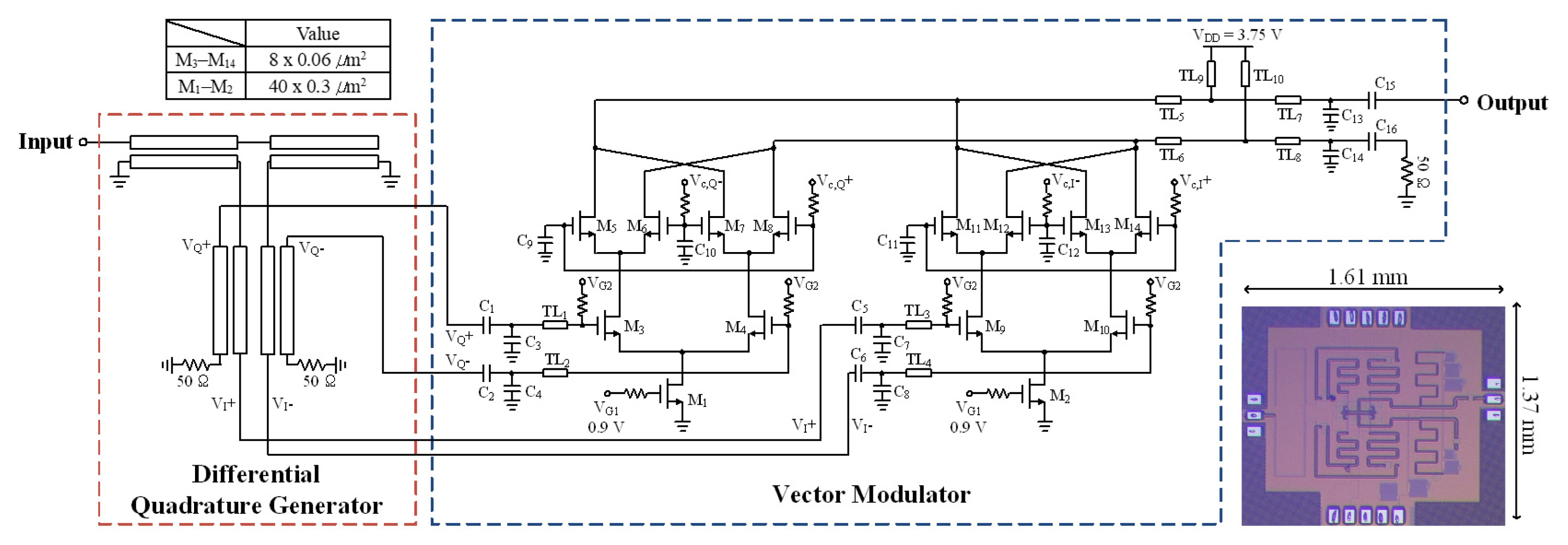
Fig. 1 shows a schematic of the proposed mm-wave VSPS. It consists of a differential quadrature generator and a vector modulator. The differential quadrature generator is implemented using a Marchand balun and two 90┬░ coupled-line couplers. Compared to the RC-CR network, this structure is robust to process and temperature variations. Four quadrature vector signals (VI+, VI-, VQ+, VQ-) are generated by feeding each balun output to an individual coupled-line coupler. The balun is implemented with two second top metals (OL) which are edge-coupled to each other. In addition, the 90┬░ coupler is implemented using the top two metals (LB and OL) which are broadside-coupled to each other.
The vector modulator employs two copies of Gilbert cell (M3ŌĆōM8 and M9ŌĆōM14). Each Gilbert cell modulates the in-phase vectors (VI+ and VI-) or the quadrature vectors (VQ+ and VQ-). By controlling the gate bias of cascode transistors (Vc,I+, Vc,I-, Vc,Q+, Vc,Q-), the amplitudes of the in-phase and quadrature signal vectors are changed individually. The differential outputs of the two Gilbert cells are combined in a current domain, thus resulting in a desired phase shift.
The input and output of the VSPS are matched to 50 ╬® with transmission lines (TL1ŌĆōTL4 and TL5ŌĆōTL8) and capacitors (C3ŌĆōC4 and C13ŌĆōC14). One of the differential outputs is terminated by an on-chip 50-╬® resistor for the convenience of measurement. A current source (M1 and M2) is connected to each Gilbert cell, which sets a constant bias current. This allows for uniform input matching performance regardless of the phase-shift states. Furthermore, the resulting high bias enhances the linearity at the expense of additional DC consumption.
The mm-wave phase shifter is fabricated in 65-nm CMOS technology. The chip micrograph is shown in the inset of Fig. 1. The chip area is 1.61 ├Ś 1.37 mm2 including all probing pads.
The measured and simulated phase shift with 4-bit resolution is shown in Fig. 2(a). It can be seen that 16 phase states achieve a full 360┬░ shift with 22.5┬░ separation from 30 to 42 GHz. Fig. 2(b) presents the simulated and measured insertion loss of the 16 phase states. The average loss is 16.3 dB at 37 GHz. The 3-dB bandwidth is 10.8 GHz (30.9ŌĆō41.7 GHz). It should be noted that the measurement is carried out under a single-ended output condition. Therefore, the insertion loss would be improved by 3 dB in principle if measured differentially. Fig. 2(c) shows the measured output power and insertion loss versus input power at 38 GHz. The average value of input-referred 1-dB compression power is 5.7 dBm at 38 GHz.
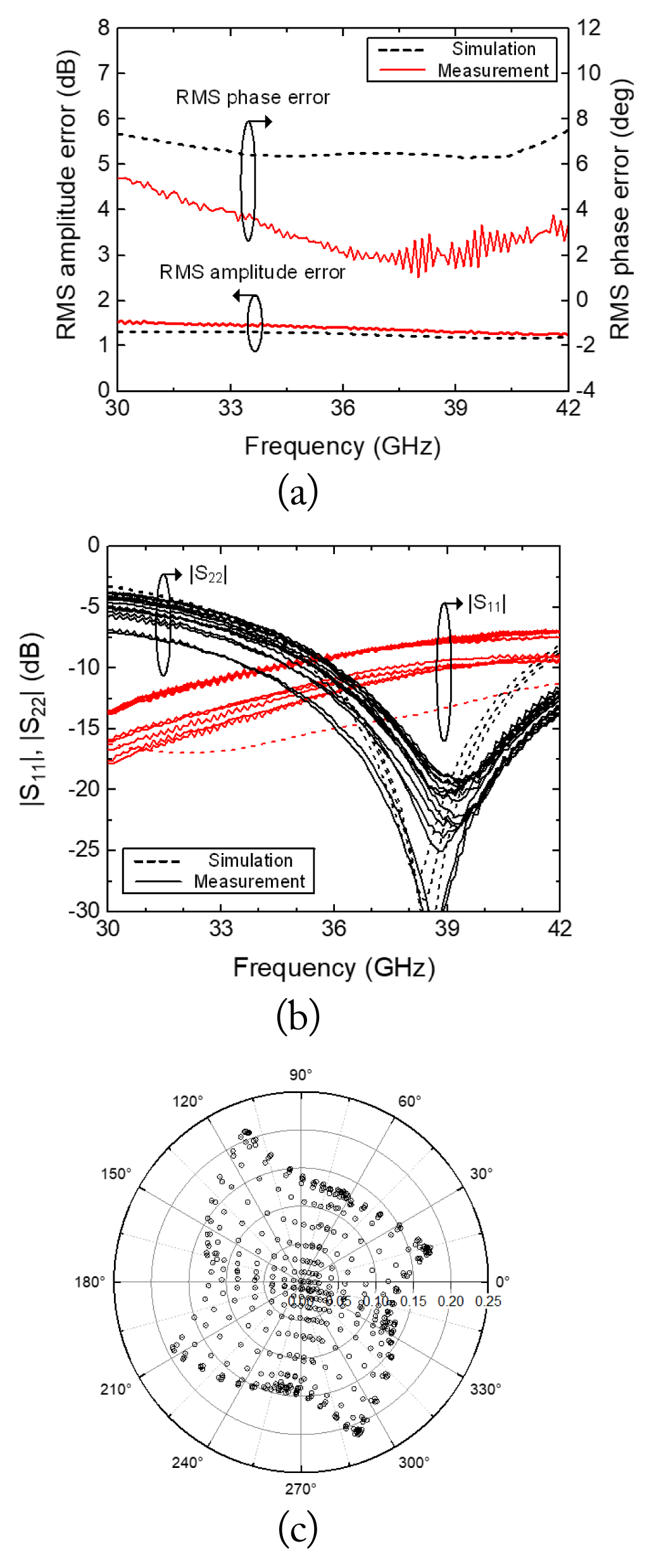
Fig. 3(a) shows the root-mean-square (RMS) amplitude and phase errors of the VSPS. With 4-bit resolution, the RMS amplitude and phase errors are 1.3 dB and 1┬░, respectively, at 38 GHz. The RMS errors maintain less than 1.5 dB and 4.9┬░ from 30.9 to 41.7 GHz. The input and output port matching performance are shown in Fig. 3(b). The input and output ports are well matched over the operating frequency.
Fig. 3(c) shows a polar plot of the measured S21 for 484 phase states. Each of the control voltages (Vc,I+, Vc,I-, Vc,Q+, Vc,Q-) is individually swept from 2.25 to 3.25 V by 0.1-V step at 38 GHz. It is noted that both the phase and amplitude can be precisely adjusted by fine tuning of the control voltages. This is a significant merit of VSPS over other phase-shifter topologies that can adjust only the phase. The DC power consumption is 45 mW at a supply voltage of 3.75 V.
In Table 1, the proposed VSPS is compared with other published phase shifters in the 5G frequency bands. The VSPS in this work achieves a wide bandwidth with comparable insertion loss and RMS amplitude and phase error. Compared to [2ŌĆō4], the proposed VSPS provides continuous phase shift and can adjust both amplitude and phase. Compared to previous VSPS [1], this work achieves a wider bandwidth and higher linearity at the cost of DC power consumption.
An mm-wave VSPS for 5G application is implemented in 65-nm CMOS technology. The VSPS exhibits a continuous 360┬░ phase shift with an average insertion loss of 16.3 dB at 37 GHz with a 3-dB bandwidth of 10.8 GHz. Compared to other VSPS in the 5G n260 band, this work achieves a wide bandwidth and high linearity. It is also demonstrated from 484 phase-state measurement that both the phase and amplitude can be adjusted in a fine resolution which is determined by the resolution of control voltage. The proposed VSPS can be adopted in various mm-wave applications including the 5G communication systems.
Acknowledgments
This work has been supported by the Future Combat System Network Technology Research Center program of Defense Acquisition Program Administration and Agency for Defense Development (No. UD190033ED).
Fig.┬Ā2
Measured (a) phase shift with 4-bit resolution, (b) insertion loss of 16 phase states, and (c) output power and insertion loss versus input power at 38 GHz.

Fig.┬Ā3
Measured (a) RMS amplitude and phase errors, (b) input and output matching of 16 phase states, and (c) polar plot of S21 for 484 phase states at 38 GHz.

Table┬Ā1
Performance comparison with previously reported phase shifters for the mm-wave 5G application
| Ref. | Tech. | Freq. (GHz) | Resolution | Avg. loss (dB) | RMS amp., phase error | Input P1dB (dBm) | Pdc (mW) |
| Chen et al. [2] | 90-nm CMOS | 36ŌĆō40 | 4 bit | 20.2ŌĆō21 | < 2.6 dB, < 2.6┬░ | - | 0 |
| Li et al. [3] | 65-nm CMOS | 32ŌĆō40 | 7 bit | 16.9ŌĆō18.1 | < 0.38 dB, < 1.6┬░ | - | 0 |
| Tsai et al. [4] | 65-nm CMOS | 27ŌĆō42 | 5 bit | 12.4 ┬▒ 1.2a | < 2.1 dB, < 3.8┬░ | 7.5b@ 39 GHz | 0 |
| Xiong et al. [1] | 90-nm CMOS | 35ŌĆō41 | Cont. | 5.9ŌĆō7 | < 0.35 dB, < 5.1┬░ | ŌłÆ2.8b@ 35.5 GHz | 17.6 |
| This work | 65-nm CMOS | 30.9ŌĆō41.7 | Cont. | 16.3ŌĆō19.3 | < 1.5 dB, < 4.9┬░ | 5.7 | 45 |
References
1. Y Xiong, X Zeng, and J Li, "A frequency-reconfigurable CMOS active phase shifter for 5G mm-wave applications," IEEE Transactions on Circuits and Systems II: Express Briefs, vol. 67, no. 10, pp. 1824ŌĆō1828, 2019.

2. CY Chen, YS Wang, YH Lin, YH Hsiao, YC Wu, and H Wang, "A 36ŌĆō40 GHz full 360┬░ ultra-low phase error passive phase shifter with a novel phase compensation technique," In: Proceedings of 2017 European Radar Conference (EURAD); Nuremberg, Germany. 2017, pp 397ŌĆō400.

Biography

Eunjung Kim received the B.S. degree in electrical engineering from Chungnam National University, Daejeon, Korea, in 2019, where she is currently working toward the Ph.D. degree in electrical and electronics engineering. Her research interest includes millimeter-wave and THz circuits for phased-array systems.
Biography

Younghwan Kim received the B.S. degree in telecommunication engineering from the Jeju National University, Jeju, Korea, in 2011, and the M.S. and Ph.D. degrees in electrical engineering from the Korea University, Seoul, Korea, in 2013 and 2020, respectively. He is currently with Samsung Electronics, Suwon, South Korea, where he is a staff engineer. His research interest includes millimeter-wave and terahertz-wave integrated circuits for phased-array wireless systems.
Biography

Sanggeun Jeon received the B.S. and M.S. degrees in electrical engineering from Seoul National University, Seoul, South Korea, in 1997 and 1999, respectively, and the M.S. and Ph.D. degrees in electrical engineering from the California Institute of Technology (Caltech), Pasadena, CA, USA, in 2004 and 2006, respectively. From 1999 to 2002, he was a full-time Instructor in electronics engineering with the Korea Air Force Academy, Cheongwon, South Korea. From 2006 to 2008, he was a research engineer with the Caltech High-Speed Integrated Circuits Group. Since 2008, he has been with the School of Electrical Engineering, Korea University, Seoul, where he is currently a professor. His research interests include integrated circuits and systems at microwave, millimeter-wave, and terahertz bands for high-speed wireless communications and high-resolution imaging applications.
- TOOLS


