I. Introduction
Frequency modulated continuous wave (FMCW) radar is a device that can calculate distances to targets even in snowy or rainy environments [1]. For a distance measurement, the FMCW radar transmitter transmits a linear frequency modulation (LFM) signal and receives the signal reflected from the target. The analog-to-digital converter (ADC) is required for the FMCW radar receiver to extract the range information by firstly multiplying the incoming signal with the transmitted signal at the mixer and then applying the fast Fourier transform (FFT) to the mixer output signal, and then finally passing the low pass filter before the ADC input is produced. Recently, FMCW radars have been utilized in Internet of Things (IOT) applications, such as vital sign detection and wireless fingerprint identification. Thus, ADCs for FMCW radar also require low power consumption and a small area. Successive approximation register (SAR) ADCs show disadvantages with respect to power consumption and layout area in proportion to the resolution of ADC [2]. Vcm (common mode voltage) based switching approach determines the sign of the differential input by connecting differential arrays to Vcm and reduces switching energy by 87.5% compared with the conventional configuration [3].
In this work, the additional voltage sources of Vref/4, 3Vref/4 were employed to improve power consumption by 98.44% and reduce capacitive digital-to-analog converter (CDAC) area by 75% compared with the conventional configuration. Additionally, in ADCs for FMCW radar, the frequency and voltage entering the input vary depending on the distance to the target. Therefore, an ADC without common mode voltage variation of CDAC is required to avoid decision error originating from the dynamic offset of the comparator. Higher-side reset-and-set (HSRS) reduces switching energy usage by 92.2% compared with the conventional scheme but has common mode voltage variation at the second cycle [4]. Vaq (the quarter of the reference voltage)-based tri-level achieves 96.48% less switching energy usage than conventional configuration based on a new third reference voltage Vaq which is a quarter of the reference voltage [5]. However, this configuration also shows a common mode voltage variation. In the proposed switching scheme, the common mode voltage is always constant during SAR operation. In terms of preventing dynamic offset, ADC using the proposed method is suitable for FMCW radar applications.
Section II introduces the proposed architecture of this work and explains the operating principle. In Section III, the switching energy for the proposed architecture is calculated and compared with circuits from previously published works. Section IV presents the implementation of key building blocks and simulation results. Generally, as shown in the AFE5401-Q1 data sheet provided by Texas Instruments, ADC for radars is applied with equalizer filters to eliminate the effect of leaked transmitted signals to the receiver. The proposed ADC is designed for transceivers with a DC offset cancellation circuit. Therefore, equalizer filters are not included in the design. In Section V, the conclusion is given.
II. Architecture & Circuit Description
In Fig. 1, the structure of the proposed SAR ADC is shown. Differential input signals are applied to the top plate of the capacitor array, and reference voltages are applied to the bottom plate of the capacitor array. The block of the SAR logic selects the switches (S1–Sn−1) of the capacitor arrays, while generating each voltage of the bottom plates. The voltage at the bottom plate of each array determines the voltage of the top plate entering the input of the comparator during the next step. This process is repeated until the final code is obtained.
Fig. 2 shows the flow chart of the working principle for the proposed N-bit SAR ADC. First, differential signals are sampled, and the sampled differential signal is applied to the input of the comparator. The comparator then decides which input shows a higher voltage. If the positive input terminal shows a higher voltage, the output of the comparator goes to the logic state “1”. The voltage of the positive input terminal of the comparator then decreases by Vref/22, while that of the negative input terminal increases by Vref/22. If the negative input terminal shows greater voltage, the output of the comparator goes to the logic state “0”. The voltage of the positive input of the comparator then increases by Vref/22, while that of the negative input decreases by Vref/22. Similarly, the second bit is determined in the next comparison. The inputs of the comparator are increased or decreased by Vref/23. This process is repeated until the Nth bit is determined.
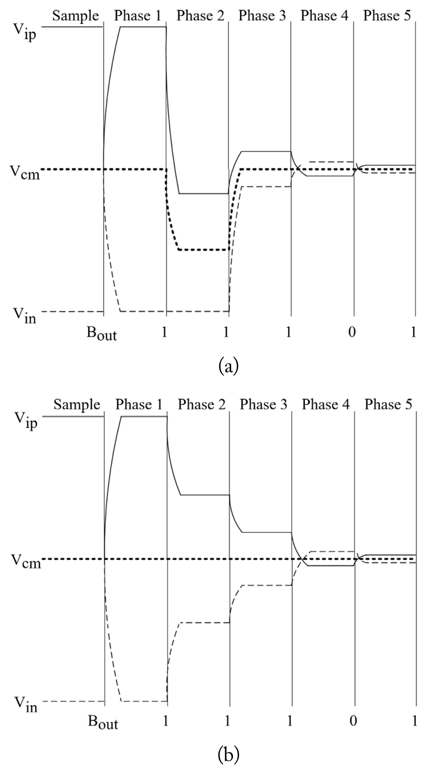
Fig. 3(a) and 3(b) show the voltage change in the top plate voltage of the capacitor array when the output of the comparator is determined to be 1,1,1,0, and 1 in order from MSB (most significant bit) in the case of the HSRS scheme and the proposed configuration. In both cases, the corresponding bits are determined according to the results of the comparator. In Fig. 3(a), the common mode level of DAC is decreased by Vref/4 in the second phase because the negative input of comparator does not change in the first phase, while the positive input is decreased by Vref/2. This variation in the common voltage generates unwanted dynamic offset and degrades the linearity of SAR ADC. On the other hand, in Fig. 3(b), the negative input of the comparator changes in the opposite direction while the positive input of the comparator changes in every phase. This means that the common mode voltage (Vcm) of the comparator input remains constant in the proposed scheme. Therefore, the proposed switching scheme minimizes the dynamic offset that eventually degrades the linearity of the SAR ADC.
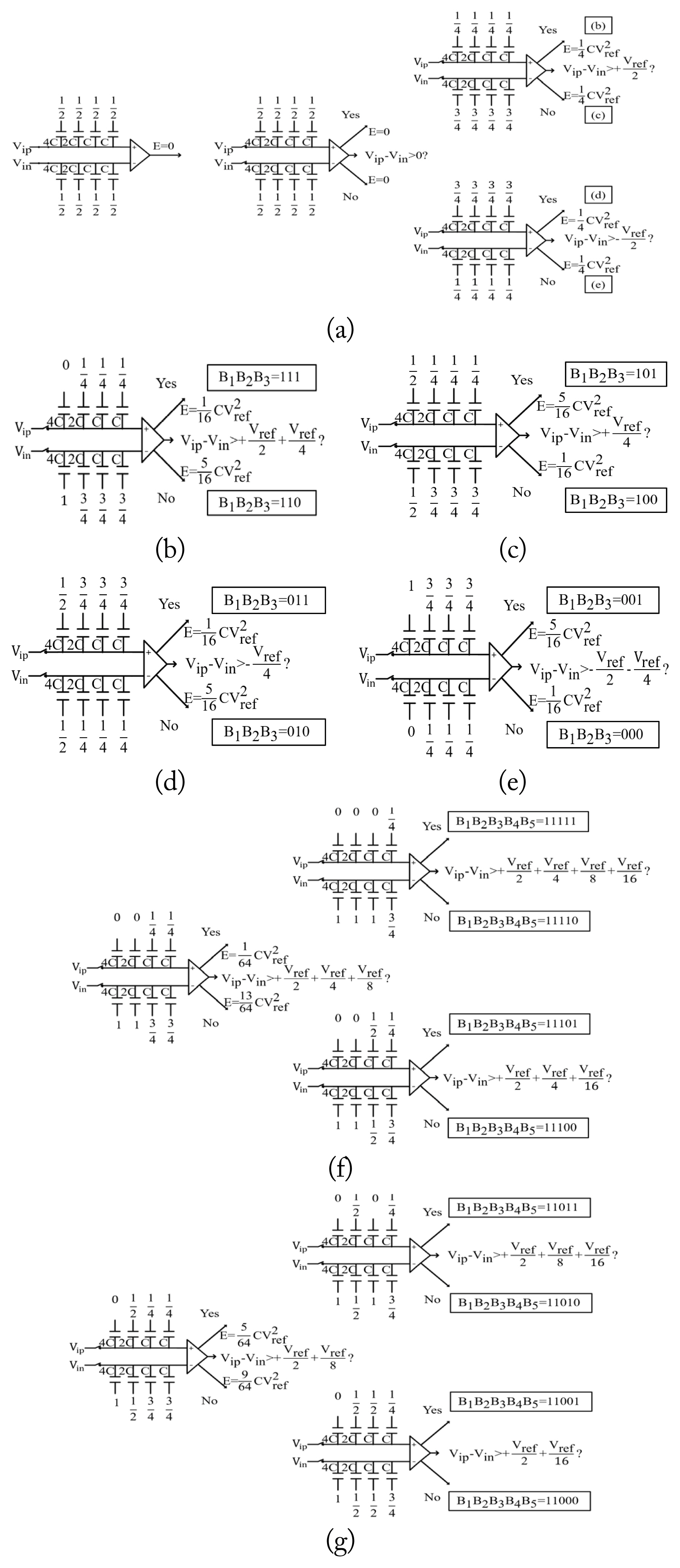
Fig. 4 illustrates the proposed switching scheme, taking an example of a 5-bit SAR ADC. In Fig. 4(a), during the sampling phase, the voltage of Vref/2 is applied to the bottom plate of the capacitor array, and the differential inputs are sampled and held onto the top plates. In the MSB decision phase, the sampling switch is turned off after the voltage of the bottom plate is set up. MSB is determined by the voltages of the sampled inputs. During the sampling and MSB decision phases, the value of the voltage source does not change, meaning that no energy is consumed in these phases. If MSB is 1, the bottom plate of the capacitor array in the positive input is connected to Vref/4, and that of the capacitor array in the negative input is connected to 3Vref/4. Because the bottom plate voltage of each array changes to the same value, the energy consumption becomes zero. The voltage of positive input of the comparator is reduced by Vref/4 compared to the previous step, and that of the negative input is increased by Vref/4 compared to the previous step; therefore, the MSB-1 bit is determined by this comparison.
If MSB is 0, the bottom plate of the positive input capacitor array is connected to 3Vref/4, and that of the negative input capacitor array is connected to Vref/4. Because the bottom plate voltage of each array changes to the same value, the energy consumption also become zero, and the voltage of the positive input of the comparator increases by Vref/4 from the previous step, while that of the negative input decreases by Vref/4 from the previous step, and the MSB-1 bit is determined by the result. Four types of decision on MSB and MSB-1 in Fig. 4(a) are explained in Fig. 4(b), (c), (d), and (e). In Fig. 4(b), the values of MSB and MSB-1 are 1 for both. The voltage of the bottom plate of the largest capacitor in the positive input is decreased by Vref/4. At the same time, the voltage of the bottom plate of the largest capacitor in the negative input is increased by Vref/4. In Fig. 4(c), the values of MSB and MSB-1 are 1 and 0, respectively. The voltage of the largest capacitor in the positive input is increased by Vref/4. At the same time, the voltage of the largest capacitor in the negative input is decreased by Vref/4. In Fig. 4(d) and 4(e), the values of MSB to MSB-1 are 01 and 00 while the voltage of the bottom plate of the capacitor array changes in the same manner, respectively.
Fig. 4(f) and 4(g) are examples of decisions when MSB to MSB-2 is 111 and 110. These figures show the decision mechanism of the lower bits in the same way. The remaining bits of the ADC are determined in a sequence of successive approximations. Fig. 4 also shows that the proposed switching scheme requires just 8-unit capacitors at each array for a 5-bit decision. For a 5-bit decision, the conventional switching scheme requires 32-unit capacitors at each array. In the case of n-bit SAR ADC, conventional scheme requires 2n-unit capacitors at each array. But proposed scheme requires only 2n−2-unit capacitors at each array. It is meant that the area reduction in the capacitor array is achieved by 75% while keeping the same resolution.
III. Calculation of Switching Energy
Energy consumption at the ith capacitor Ci (i = 1,...,n) in the transition of (a) to (b) can be calculated as shown in Eq. (1) where VBOT(b)_i is voltage applied to bottom plate of the Ci at (b) state, ΔQi is difference of charge at Ci and ΔVi is difference of voltage at Ci during the transition. Thus, Eq. (2) can be induced from Eq. (1).
The total energy consumption in the transition of (a) to (b) can be expressed as in Eq. (4).
In Fig. 4, the energy consumption of each transition is calculated using the Eq. (3) and Eq. (4). For example, in Fig. 4(f), when the comparator decision result is 1, the energy consumption of capacitor array at the positive comparator’s input is shown in Eq. (5), where Ei is energy consumption at the ith large capacitor.
The energy consumption in the negative input capacitor array is shown in Eq. (6).
Thus, as shown in Fig. 4(f), the total energy consumption of the positive and negative arrays is CV2ref/64.
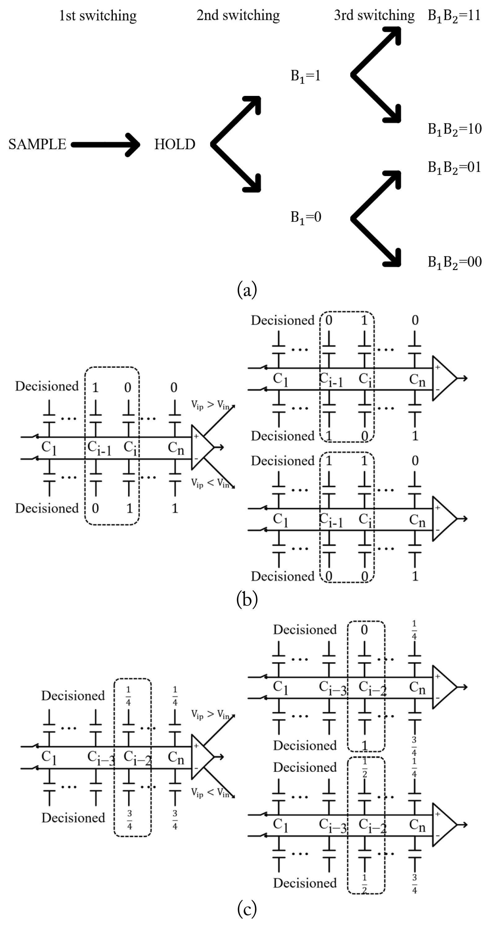
Fig. 5(a) shows an example of CDAC switching from each phase of the SAR ADC to the next phase. CDAC operates to increase or decrease the top plate voltage of the capacitor array by Vref/2i according to the result of the comparator during the ith switching phase. Fig. 5(b) shows the ith switching step of the CDAC in the conventional method. In this case, the voltage applied to the bottom plate remains unchanged except for Ci−1, Ci. In the process of adding all the energy consumptions in the case that for 2i−1 in the ith switching step using Eq. (3), the energy consumption of the bottom plate without voltage change is canceled out and does not contribute to the result of the average energy consumption. Therefore, the average energy consumption is expressed in Eq. (7) by using Eq. (3) for two cases where the bottom plate voltage changes in Ci−1 and Ci.
(7)
In the case of N-bit SAR ADC, the number of unit capacitors required per array in the conventional method is 2N, which can be represented by Ci = 2N−iC where C is the unit capacitance of CDAC. This can be used to represent Eq. (7) as shown in Eq. (8).
Thus, the average switching energy for the N-bit SAR ADC using the conventional switching scheme can be derived as shown in Eq. (9).
Fig. 5(c) shows the ith switching step of the CDAC in the proposed method. In this case, the voltage applied to the bottom plate remains unchanged except for Ci−2. Thus, as in the conventional method, the average energy consumption is derived as in Eq. (10) considering two cases where the bottom plate voltage changes in Ci−2 using Eq. (3).
For the N-bit SAR ADC, the number of unit capacitors required per array in the proposed method is 2N−2, which can be represented by Ci = 2N−i−2C, where C is the unit capacitance of CDAC. This can be used to represent Eq. (10) as Eq. (11).
Thus, the average switching energy for the N-bit SAR ADC using the proposed switching scheme can be derived as shown in Eq. (12).
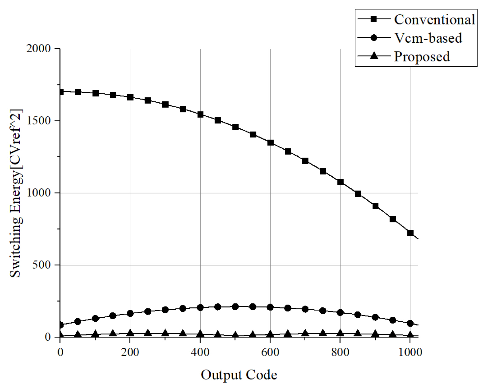
Using Eq. (9) and Eq. (12), when the resolution is 10 bits, the conventional switching scheme consumes 1363.3CV2ref energy on average, and the proposed switching technique consumes 21.208CV2ref energy on average. Therefore, for the 10-bit ADC, energy consumption can be reduced by 98.44%.
Fig. 6 shows the switching energy consumed by the conventional switching scheme, the Vcm-based method, and the proposed switching scheme, respectively, when the resolution is 10 bits.
In Table 1, the performance with various switching procedures for 10-bit ADC is compared. The proposed switching scheme reduces switching energy consumption by about 98.44%. Also, the proposed switching method reduces the number of unit capacitors of the CDAC array to 1/4 of the conventional method. Capacitors of CDAC take up the dominant area for CDAC layout; therefore, the CDAC area is reduced by 75%.
IV. Circuit Implementation
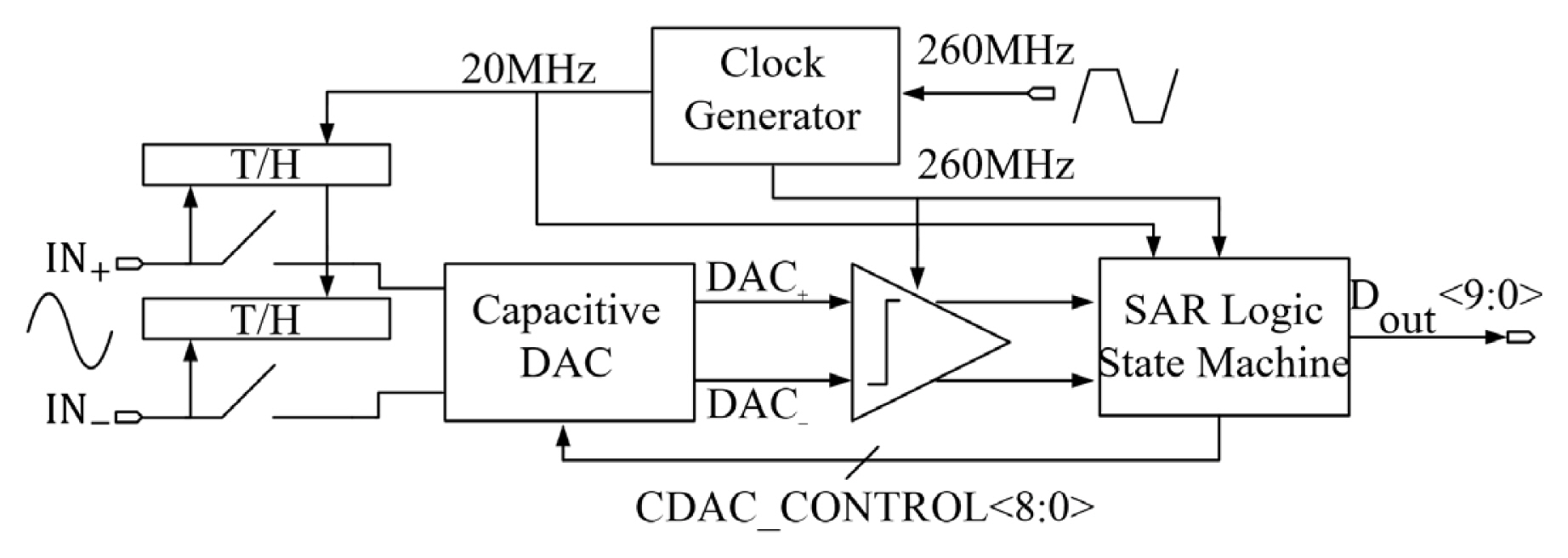
Fig. 7 shows the top-level architecture of the proposed 10-bit ADC. The input frequency of the clock generator is 260 MHz, and the ADC operates at a sampling rate of 20 MS/s. The fundamental building block of the proposed ADC consists of a track-and-hold (T/H) circuit, a dynamic comparator, SAR control logic, and CDAC.
In a simple N-MOS T/H circuit, Ron of N-MOS shows approximately [μnCox(W/L)(VDD-Vin-VTH)]−1, so the input range is limited as Vin approaches VDD-VTH. To improve on this, a complementary switching scheme is employed as the T/H circuit.
The designed ADC applied the dynamic comparator [6]. By using positive feedback, the comparator output operates in such a way that one side is determined to be VDD and the other to be zero.
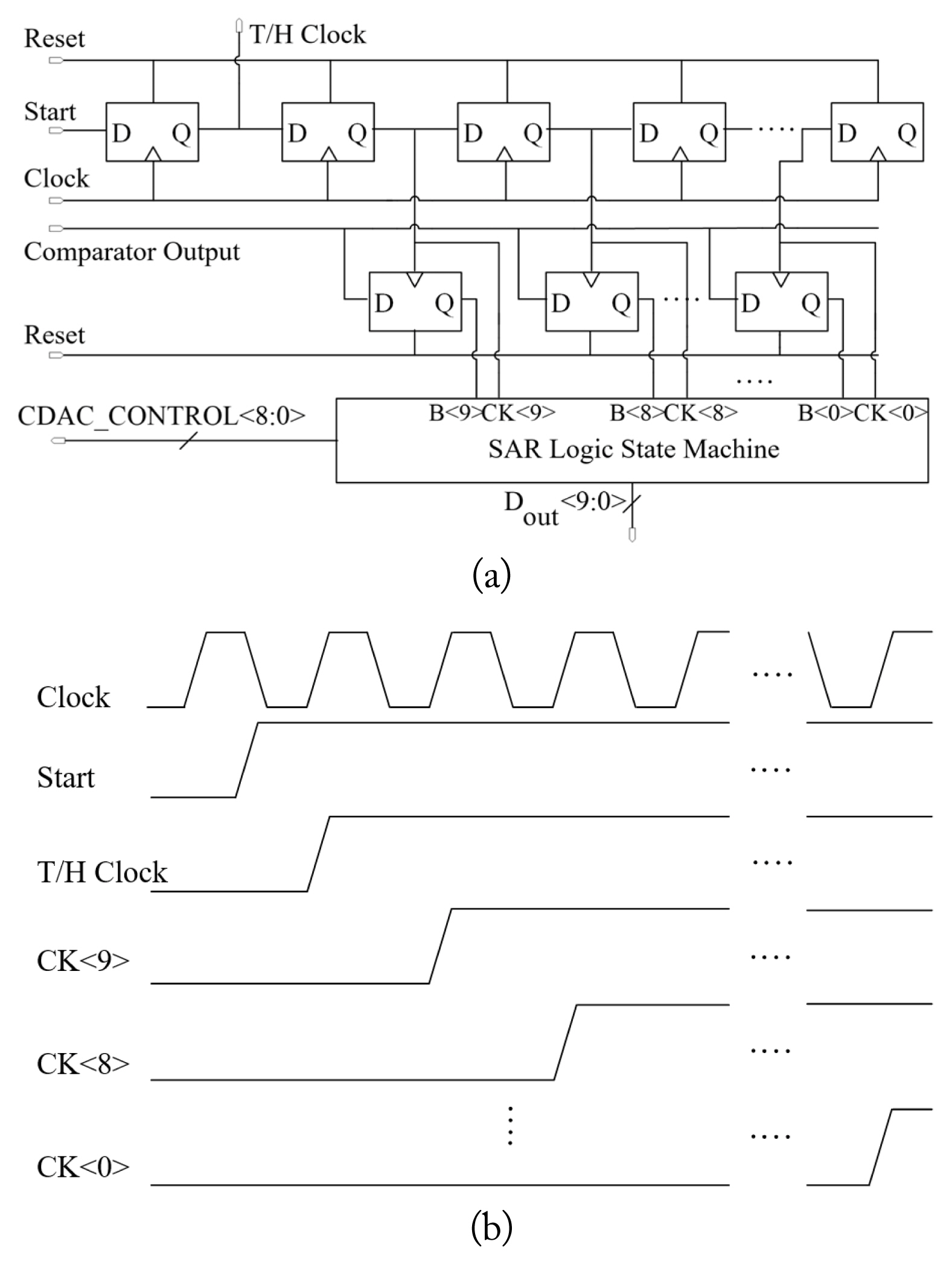
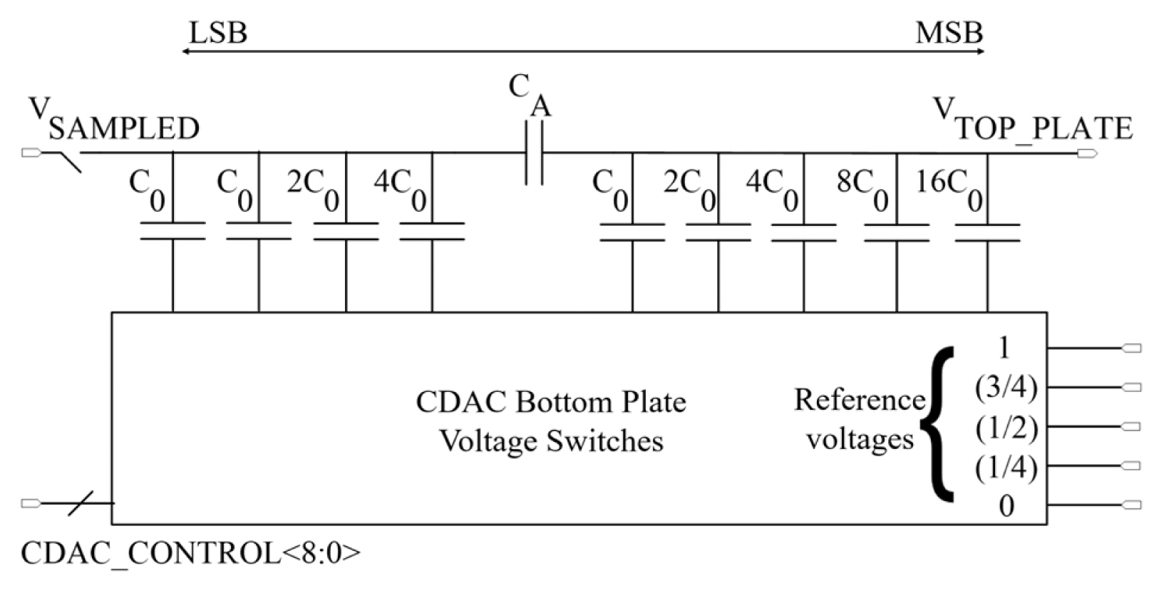
Fig. 8 shows the SAR logic and timing diagram generated from the proposed ADC design. When a start signal is applied at any instant, a clock signal of T/H block is generated to hold the input signal sampled at the next clock edge. At the next clock edge, CK<9> occurs so that flip-flops can get the first decision result of the comparator, and then at the clock edge after that, CK<8> is generated sequentially. This logic is repeated until CK<0> is generated. Each decision result of the comparator is stored in each flip-flop. These results are successively reentered to the SAR logic state machine with CK<9:0>. The SAR logic state machine outputs Dout<9:0>, the final conversion result of the ADC. The SAR logic state machine also produces CDAC_CONTROL<8:0>, which controls the bottom plate voltage of the CDAC, as shown in Fig. 9. Fig. 9 shows a schematic of the CDAC. In the CDAC bottom plate voltage switches, voltage at the bottom plate of the CDAC is determined by the CDAC_CONTROL signal as one of five reference voltages (0, Vref/4, Vref/2, 3Vref/4, and Vref) until the 10-bit decision is complete. An example of switching is shown in Fig. 4. To solve the problem of the CDAC’s total capacitance increasing exponentially as the resolution of ADC increases, the attenuating capacitor scheme is employed, as shown in Fig. 9 [7]. The size of the CA is determined by Eq. (13) where C0 is 208 fF.
Thus, in Fig. 9, the least significant bit (LSB)-side capacitors viewed from the MSB side of the capacitor array appear to be attenuated by the CA by 23. That is, when switched to an equivalent conventional weighted capacitive array, the unit capacitance appears to be C0/8, which reduces power consumption and the RC time constant. The ideal power consumption of the reference voltage at the proposed ADC is equal to Eq. (14).
Since the designed ADC has a 10-bit resolution, to use Eq. (12)Eavg,proposed is deduced to be 21.208CV2ref. At a 1.2-V reference voltage and 20 MS/s sampling rate, if the effective unit capacitance by attenuation capacitor is 26 fF, the expected power consumption per conversion is calculated as 0.015 mW. The simulation result of average power consumption per conversion at the reference voltage sources is 0.02 mW because the switch at bottom plate in CDAC consumes dynamic current during transitions.
Fig. 10 shows the overhead that occurs when an additional reference voltage is used. State-of-the-art ADCs use two reference voltages, Vref and Vref/2, so the proposed switching scheme requires two additional voltage followers for 3Vref/4 and Vref/4 reference voltage sources. This acts as an additional overhead in terms of the area and power consumption of the ADC. For example, if a voltage follower is constructed using a single-stage op-amp with a power consumption of 4.8 μW, the ADC using the proposed scheme consumes an additional 9.6 μW compared to the state-of-the-art ADCs. In case of area overhead, an area of 10 μm2 for each op-amp should be considered. We also consider a load capacitor size of 50 μm2 to mitigate the impact of clock feedthrough on N-MOS switches. Thus, two additional voltage followers are used, requiring an additional area of 120 μm2. Area overhead will not be much of a constraint given that the size of the unit capacitor used in this design is 100 μm2.
The simulated results of differential nonlinearity (DNL) and integral nonlinearity (INL) of the proposed ADC are shown in Fig. 11. The maximum DNL and INL are 0.44/−0.49 LSB and 0.5/−0.5 LSB, respectively. The simulated dynamic performance is shown in Fig. 12. An input frequency close to 5 MHz is chosen in consideration of FFT’s coherent sampling. The simulated SINAD (signal-to-noise and distortion ratio) and SFDR (spurious free dynamic range) are 42.11 dB and 42.63 dB at 20 MS/s sampling rate, respectively.
V. Conclusion
The switching technique of SAR ADC for FMCW radar transceivers using quarter reference voltages is proposed. The proposed switching scheme has the benefits of energy consumption and area reduction, suitable for use as an ADC for radar transceivers. This technique has the additional benefit of improving the linearity of SAR ADC, because employing additional reference voltages minimizes the unwanted dynamic DC offset at the input of the comparator. The designed ADC focuses on implementing the proposed switching method to verify that it keeps the simulated switching energy result consistent with the calculation one. Further applications of the technique will improve the dynamic performance of ADC and it will also increase the utilization in FMCW radar transceivers.


