 |
 |
- Search
| J. Electromagn. Eng. Sci > Volume 22(3); 2022 > Article |
|
Abstract
In this Letter, analytic models for EM radiation analysis of a microstrip line (trace) on a slotted ground plane are proposed. The EM radiation is separated by the effects of trace and slot, and analytic radiation models for each effect are presented. The radiated electric field in the far region is calculated at a frequency up to 10 GHz, and the effect of the slot size on the radiation is examined. The proposed models are in good agreement with the numerical results while requiring a negligible computation time.
As electronic devices operate at higher frequencies, concerns about unwanted electromagnetic (EM) radiation from printed circuit boards (PCBs) are also increasing. When a high-speed signal passes over a slotted ground plane, the radiation, as well as the crosstalk between signals, increases. This is a typical PCB-level EM interference problem that has been studied for a long time. In [1], crosstalk and radiation that occur when a signal line passes through a split reference plane in a high-speed multilayer PCB were analyzed using a slot waveguide model. Recently, an EM radiation model of a stripline with a slotted ground plane using a partial-element equivalent-circuit method was proposed [2]. These methods focused on the crosstalk between signals and applied numerical methods to calculate the radiation.
In this Letter, analytic models for EM radiation analysis of a microstrip line on a slotted ground plane are proposed. Using these models, the radiation mechanism can be intuitively understood, and accuracy similar to that of a numerical simulation can be obtained by a quick calculation.
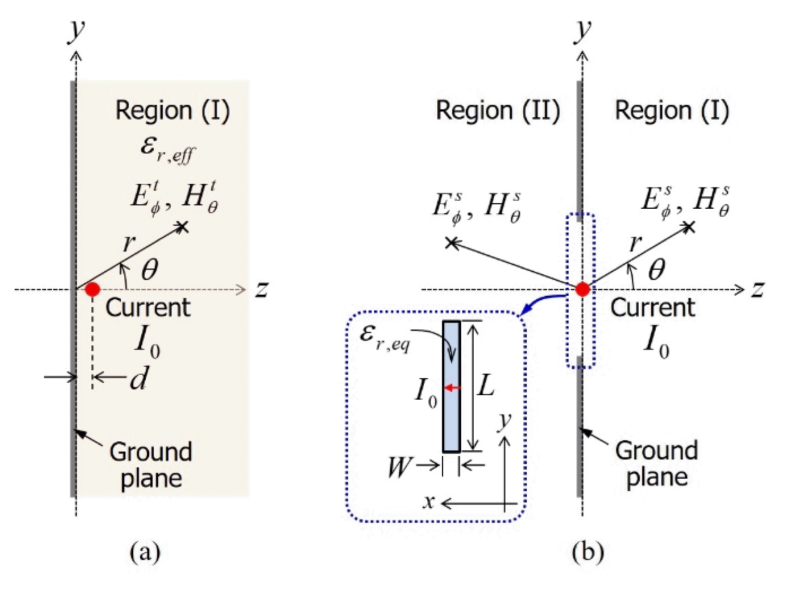
Fig. 1 shows the structure of a microstrip line (trace) passing over a slotted ground plane. The radiated fields can be calculated by dividing region (I) over the microstrip line and region (II) over the ground plane. In this paper, as shown in Fig. 2, the trace and slot radiation models were separately derived and calculated. Therefore, the radiated field in region (I) can be expressed as the sum of the trace and slot radiations, and the radiated field in region (II) can be expressed by the slot radiation as follows:
The magnetic fields are obtained by
H ╬Ė I , I I = E Žå I , I I / ╬Ę 0
First, when a microstrip line is terminated with a resistor equal to its characteristic impedance, the radiated electric field in the far region by the microstrip line can be expressed as follows [3]:
where I0 is the current flowing along the trace, l is the length of the trace, d is the thickness of the dielectric substrate,
╬▒ = ╬Ą r , e f f - sinŌĆē ╬Ė ŌĆē cos Žå , ŌĆē k 0 = Žē ╬╝ 0 ╬Ą 0
where tw is the width of the trace.
Next, let us look at the slot radiation model. As shown in Fig. 2(b), a long slot is L├ŚW of the length and width, and it lies long along the y-axis. When the direction of the microstrip line and the slot are perpendicular to each other, EM coupling becomes the maximum and then EM radiation by the slot is the greatest. Recently, the radiated field from a long slot induced by an infinite line current was calculated using an equivalent magnetic dipole moment on the slot [5]. However, this method is inaccurate in the microstrip structure, where the line current and the slot on a ground plane are remarkably close to each other. Therefore, we propose a slot antenna model excited by a current source, which is the microstrip line current, to be directly applied to the slot, as depicted in Fig. 2(b). In the radiation model of a slot antenna, a voltage source is typically applied to the center of the slot [6]. However, this study employs a current source. The radiation equation of the slot antenna is modified as:
where
k e q = Žē ╬╝ 0 ╬Ą 0 ╬Ą r , e q
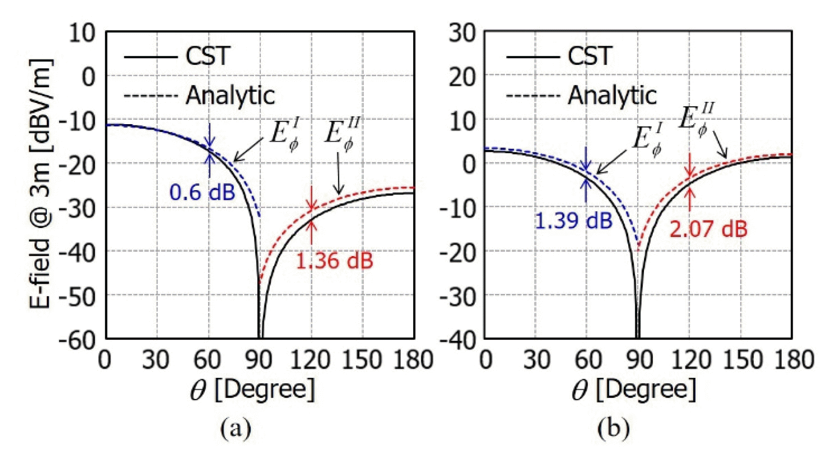
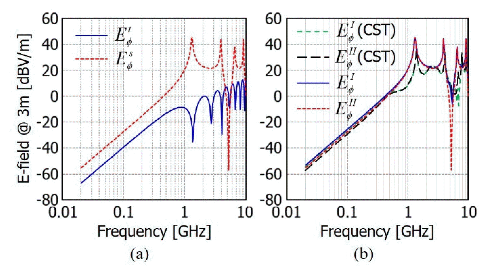
To verify the accuracy of the proposed radiation models,
E Žå t E Žå s E Žå I E Žå I I E Žå I E Žå I I E Žå I E Žå I I
Table 1 shows the computation time required to obtain the results in Fig. 4. When using an ordinary PC (Intel Core i5-7500 and 8-GB memory), the computation time of the analytic models is less than 2 seconds, while that of the numerical simulation is more than 13 minutes. This implies that the proposed analytic models are computationally efficient, as well as accurate.
Analytic models for the radiation analysis of microstrip lines on a slotted ground plane were proposed. The radiation was separated by the effects of trace and slot, and the radiated electric field in the far region was examined in terms of the slot size up to 10 GHz. The proposed models were in good agreement with the numerical results while requiring a negligible computation time.
Acknowledgments
This work was supported by the Institute of Information & Communications Technology Planning & Evaluation (IITP) grant funded by the Korea Government (MSIT) (2020-0-00839, Development of Advanced Power and Signal EMC Technologies for Hyper-Connected E-Vehicle).
Fig.┬Ā1
Problem of electromagnetic radiation from a microstrip line on a slotted ground plane. (a) Perspective view. (b) Cross-sectional view.
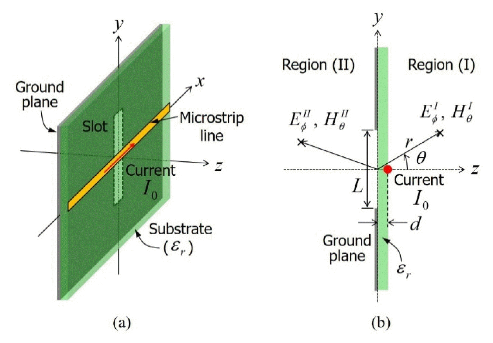
Fig.┬Ā3
Radiated electric fields of case 1. (a) Trace and slot radiations. (b) Total radiations in regions (I) and (II).
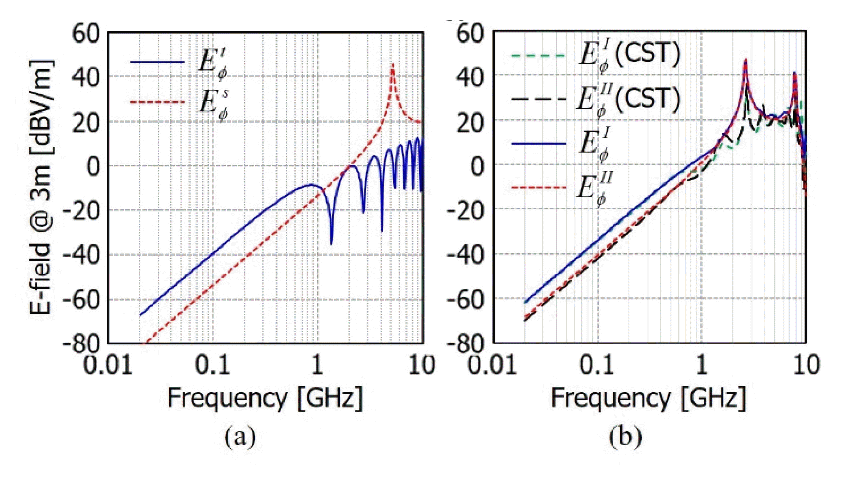
Fig.┬Ā4
Radiated electric fields of case 2. (a) Trace and slot radiations. (b) Total radiations in regions (I) and (II).
Table┬Ā1
Comparison of computation times for Fig. 4
| Analytic models | Numerical method (CST) |
|---|---|
| 1.51 sec | 13 min 45 sec |
References
1. J Kim, H Lee, and J Kim, "Effects on signal integrity and radiated emission by split reference plane on high-speed multilayer printed circuit boards," IEEE Transactions on Advanced Packaging, vol. 28, no. 11, pp. 724ŌĆō735, 2005.

2. L Ye, X Sun, T Huang, Y Sun, S Jin, B Chen, and J Fan, "Modeling stripline with slotted ground plane in multilayered circuit board using PEEC formulation," IEEE Transactions on Electromagnetic Compatibility, vol. 62, no. 1, pp. 280ŌĆō284, 2020.


3. M Leone, "Closed-form expressions for the electromagnetic radiation of microstrip signal traces," IEEE Transactions on Electromagnetic Compatibility, vol. 49, no. 2, pp. 322ŌĆō328, 2007.

4. KC Gupta, R Garg, IJ Bahl, and P Bhartia, Microstrip Lines and Slotlines, Artech House. 1996.
5. S Woo and HH Park, "Analytic model of electromagnetic radiation from a slot on conducting plane excited by common-mode current of a cable," Journal of Korean Institute of Electromagnetic Engineering and Science, vol. 31, no. 7, pp. 651ŌĆō654, 2020.
6. A Ishimaru, Electromagnetic Wave Propagation, Radiation, and Scattering: From Fundamentals to Applications, John Wiley & Sons. 2017.


