 |
 |
- Search
| J. Electromagn. Eng. Sci > Volume 22(3); 2022 > Article |
|
Abstract
Parallel loop feed structures can be used to implement wideband impedance. However, when a parallel loop feed structure is employed, parasitic resonance occurs in certain feed structures, resulting in the degradation of radiation efficiency. This is caused by the inductance and capacitance of the shunt line that is added to achieve the wideband impedance. We compared two antennas, one with a high impedance level and another with a low impedance level, by adjusting the ratio of the inductance to the capacitance of the parasitic resonance. When the parasitic resonance has a high impedance level, there is an improvement in the impedance bandwidth as well as the radiation efficiency of the antenna.
In recent times, mobile devices have become increasingly smaller, requiring a miniaturized antenna. In addition, a wide-band high-efficiency radiation performance is also required. To ensure this performance, many studies have been conducted on wideband antennas. The miniaturization of the antenna was achieved with a conventional planar inverted-F antenna (PIFA), but the wideband characteristic was not [1]. To achieve the wideband characteristics, planar inverted-E (PIE) antennas with an impedance bandwidth that has been improved by up to two or three times have been studied recently [2ŌĆō4]. It was observed that their efficiency characteristic was aggravated in some cases even though their impedance bandwidth was extended. It was found that their efficiency improved according to the impedance characteristic of their feed structure [4]. However, in several studies on the efficiency of PIE antennas, it was observed that their efficiency was reduced to zero at a specific frequency and that the frequency was controlled by the dimension of the specific point of the PIE feeding structure. These PIE antennas are designed by adding shunt capacitors to conventional PIFA feed structures. When a feed structure for a wideband antenna is implemented using a shunt capacitor in a PIFA, parasitic resonance can occur. This is due to the distributed inductance of the shunt line and the shunt capacitor in a certain shape of the feed structure. At the parasitic resonant frequency, an efficiency null phenomenon occurs, during which the efficiency is reduced to almost 0%. This null efficiency affects the efficiency and the bandwidth of the antenna when it is close to the frequency at which the antenna is operating.
In this study, a shunt capacitor was added to PIFA and a lumped inductor was added to the shunt line to improve the efficiency of the antenna operating frequency. This reduced the bandwidth of the null efficiency by changing the impedance level of the parasitic resonance [5]. The operation mechanism of the proposed resonant feeding structure can be well investigated using the two-port network impedance matrix. The basic concept of the two-port network was introduced well in [6]. Two antennas were proposed to compare their characteristics under the influence of the parasitic resonance. The elements, ground planes, and feed structures of these two antennas had the same size and shape. To change the impedance level of the parasitic resonance, a lumped inductor was added to the shunt capacitor line in antenna 2 alone. As a result, this antenna was able to significantly reduce the parasitic resonance bandwidth and improve the average efficiency. We present the details of the proposed antenna design and demonstrate an improvement in the impedance bandwidth and radiation efficiency performance through the simulation and experiment results.
The geometries of the two antennas are shown in Fig. 1. The printed circuit boards (PCBs) were all made of Flame Retardant 4 (FR4) substrate (╔ør = 4.4, tan╬┤ = 0.02) with copper. Each of these antennas comprised a ground plane, a feed structure, and a radiating element. The size of the ground plane was 100 ├Ś 50 mm2 with a clearance of 20 ├Ś 50 mm2 to set up an antenna. The feed structure was a parallel resonator that included a feed line, a shorting line, and a shunt capacitor line. The dimensions of the feed structure were 6 ├Ś 5.5 mm2, with a shunt capacitor.
Fig. 2 shows the operating principle of the feed structure of the proposed antenna. The current mode of the proposed antenna differs from that of the PIFA in terms of its feed structure due to the addition of the shunt line with a capacitor. The shunt line, including a capacitor and an inductor, is located between the shorting line and the source. In the PIFA feed structure, only one loop current is formed along the loop of the shorting pin and the source. When the shunt line is added, two loop currents can be formed. current I1 comprises the loop of the shunt line and the source, and current I2 comprises the loop of the shorting line and the shunt line. I1 is excited by the source, and I2 is excited by I1. The wideband performance can be achieved as the new loop current I2 resonance is added to the conventional PIFA. The magnitude of the loop current I2 can be controlled by the voltage across the shunt line, that is, by the overlap current in Fig. 2. The two loop circuits are represented by the following two-port impedance matrix [6]:
Here, Zf1 and Zf2 are the impedances of feeding loop 1 and feeding loop 2, respectively. Zsh is the impedance of the shunt line. As seen in Eq. (1), the degree of coupling is determined by the magnitude of Zsh. During the operation of the PIE feed structure, the resonant frequency of feeding loop 2 is set at the operating frequency of the antenna. However, Zsh is included in feeding loop 2 and forms a series resonance because of the inductance and capacitance of the shunt line. Generally, the series resonant frequency is higher than the operating frequency because the shunt line is part of feeding loop 2. At Zsh = 0, there is no coupling between the two feeding loops. As a result, power cannot be transferred from the feeding structure to the antenna element because I2 has barely been generated on feeding loop 2. Therefore, if this parasitic resonance of Zsh = 0 is designed close to the operating frequency, the obtained impedance bandwidth and efficiency will be degraded.
The resonant frequency and the bandwidth characteristics of the parasitic resonance is determined by the distributed inductance on the shunt line and the shunt capacitor. In this case, when the resonant frequency of the parasitic resonance is close to the operating frequency of the antenna, since power cannot be transferred from the feeding structure to the radiator, the impedance bandwidth of the antenna becomes narrow and the efficiency decreases. Therefore, the parasitic resonance should be designed to have a narrow bandwidth characteristic to minimize the effect on the antenna. The parasitic resonance should have a high impedance level to have a narrow impedance bandwidth. The impedance level of the parasitic resonance is defined
Eq. (2) shows the reactance differential of impedance in the parasitic resonant frequency. In this equation, ŌłéXsh/ŌłéŽē represents the input reactance change in the resonant frequency of the shunt line. When the reactance changes rapidly at the resonance frequency, it has a high impedance characteristic and a narrow impedance bandwidth. Lsh is the distributed inductance on the shunt line, and Csh is the lumped capacitor on the shunt line. Žēsh is the resonance frequency determined by the distributed inductance of the shunt line and the lumped capacitor. As can be seen from the equation, the impedance bandwidth characteristic of the parasitic resonance can be determined by controlling the ratio of the distributed inductance on the shunt line and the shunt capacitor. If the inductance is large and the capacitor is small at the parasitic resonance frequency, the variation of the stored energy becomes large and results in a narrow impedance bandwidth characteristic. Antenna 2 intentionally inserts a lumped inductor in the shunt capacitor line to control the impedance characteristic of the parasitic resonance. In antenna 1, the parasitic resonance demonstrates a wide impedance bandwidth characteristic by using a large capacitor of 6.5 pF without a lumped inductor. At the same frequency where the parasitic resonance of antenna 1 occurs, a 7 nH lumped capacitor of 2 pF was applied to the lumped inductor of antenna 2 to observe the change in the antenna characteristics when the parasitic resonance had only a change in the high impedance characteristic. A 7 nH lumped inductor and a 2 pF capacitor were used in antenna 2, so the parasitic resonance demonstrated a narrow impedance bandwidth characteristic.
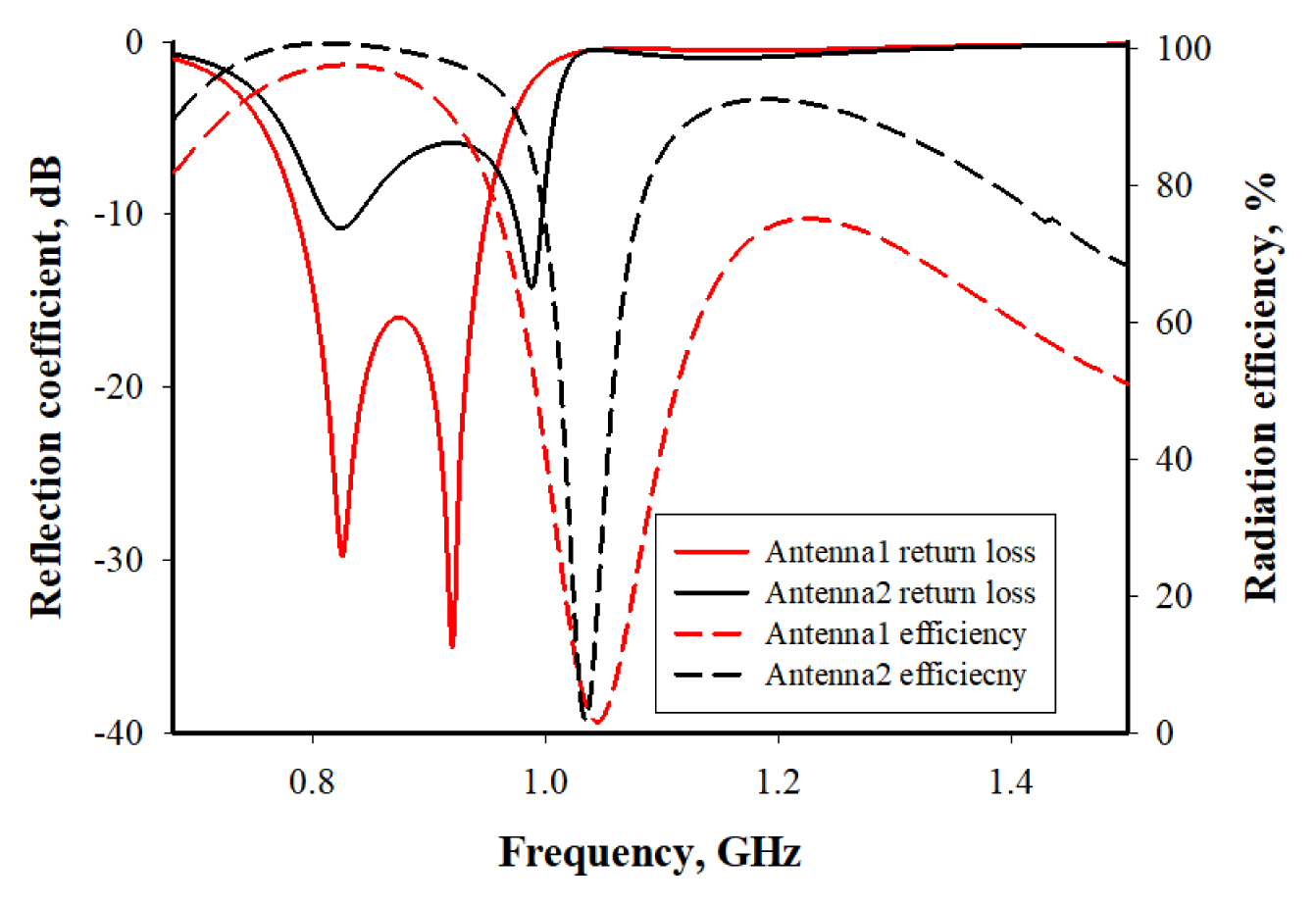
The simulated reflection coefficient and the radiation efficiency are shown in Fig. 3. Due to the differences in the bandwidth characteristic of the parasitic resonance of the two antennas, a difference occurred in the impedance bandwidth as well. Antenna 1 operated at a bandwidth of approximately 180 MHz based on a voltage standing wave ratio of 3:1. Antenna 2 operated at a bandwidth of approximately 220 MHz. With regard to the radiation efficiency, the null efficiency was confirmed at approximately 1.03 GHz. It was observed that the bandwidth difference of the null efficiency between antenna 1 and antenna 2 was in accordance with the impedance characteristic of the parasitic resonance. Antenna 1 demonstrated approximately 74% efficiency at 960 MHz, and antenna 2, approximately 93%.
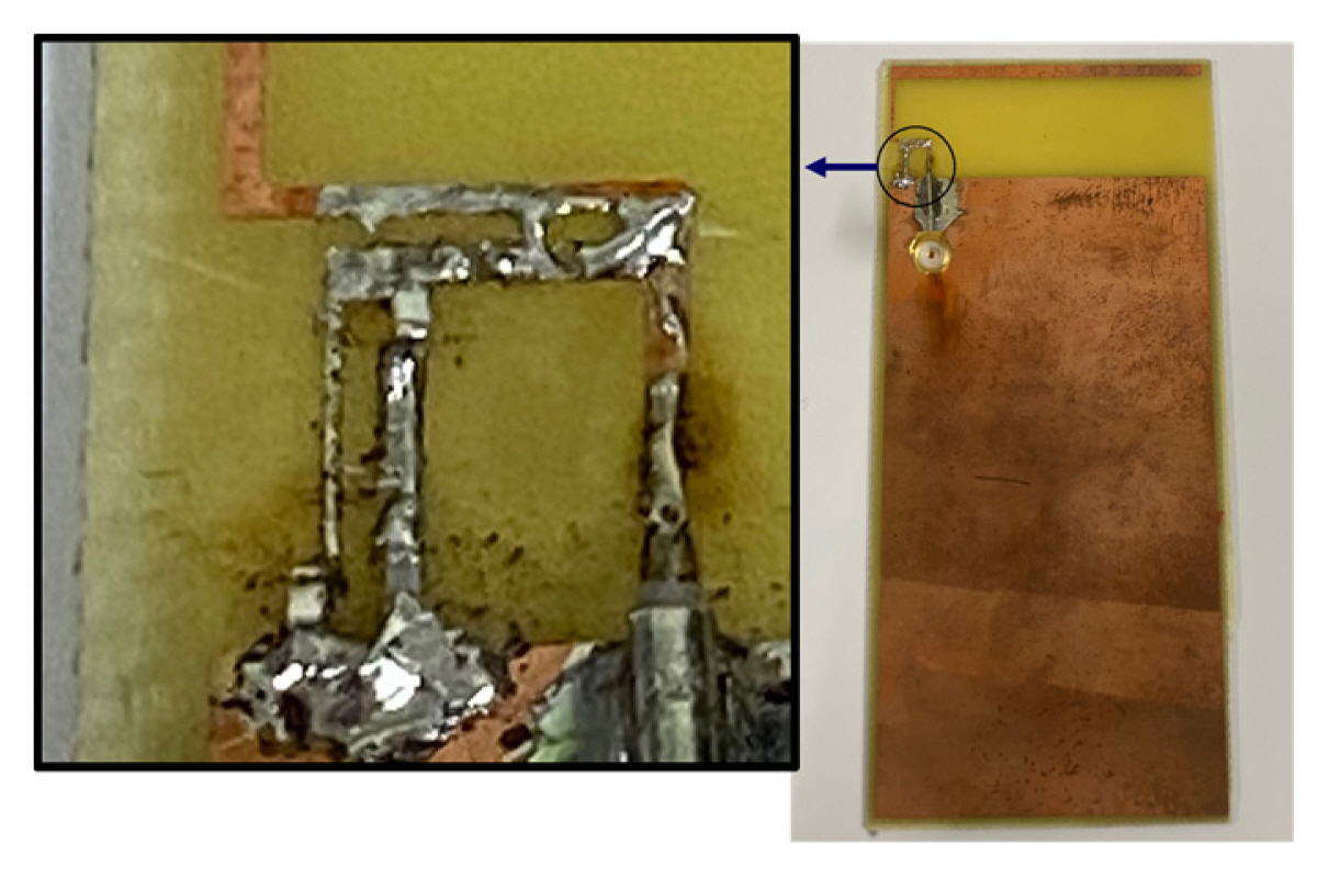
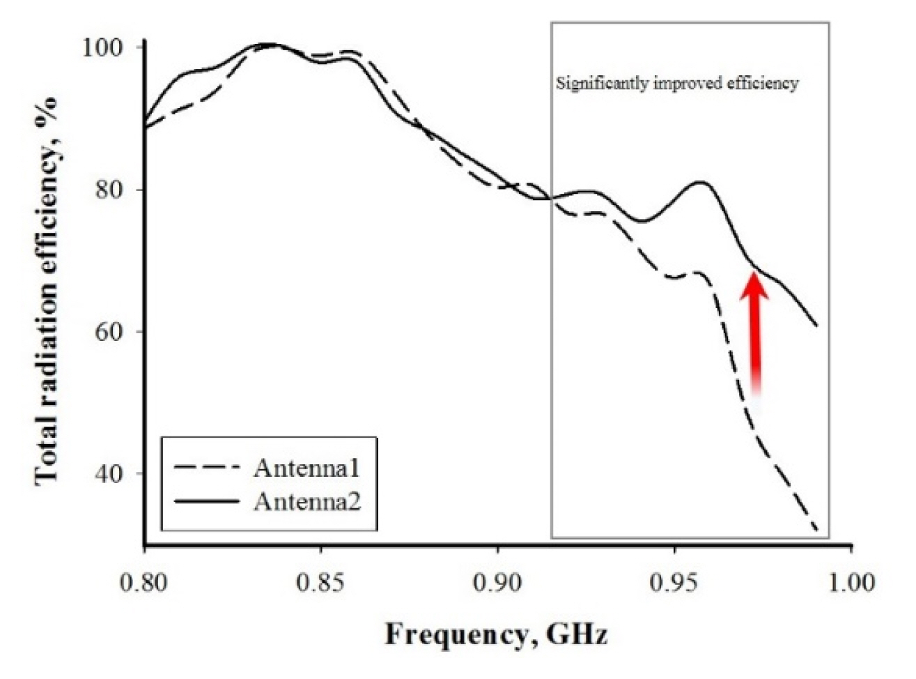
The fabricated antenna prototype is shown in Fig. 4. The measured total efficiencies, including the reflection coefficients, of the two antennas are shown in Fig. 5. The measured results are in good agreement with the simulation results. The efficiency of antenna 1 is significantly lower than that of antenna 2. Especially at 990 MHz, the efficiencies of antenna 1 and antenna 2 were 32% and 66%, respectively, which indicate that the efficiency of antenna 2 was 34% higher than that of antenna 1.
In this study, we improved the radiation efficiency and the impedance bandwidth of antenna 1 by controlling the impedance characteristic of the parasitic resonance in the parallel feed structure. At the parasitic resonant frequency, the radiation efficiency approached 0%. Generally, this parasitic resonance frequency occurred near the antenna operating frequency. Thus, the parasitic resonance should have a narrow bandwidth characteristic because if its bandwidth is wide, it affects the antenna. When the parasitic resonance is designed to have a higher impedance level, it has a narrow impedance bandwidth. Thus, an antenna with a wider impedance bandwidth and higher radiation efficiency can be obtained.
Acknowledgments
This study was supported by the National Research Foundation of Korea through a grant from the Korean government (Ministry of Science and ICT) (No. 2019 R1F1A1063993).
References
1. JS McLean, "A re-examination of the fundamental limits on the radiation Q of electrically small antennas," IEEE Transactions on Antennas and Propagation, vol. 44, no. 5, pp. 672ŌĆō676, 1996.

2. S Jeon, Y Liu, S Ju, and H Kim, "PIFA with parallel resonance feed structure for wideband operation," Electronics Letters, vol. 47, no. 23, pp. 1263ŌĆō1265, 2011.

3. S Jeon and H Kim, "Mobile terminal antenna using a planar inverted-e feed structure for enhanced impedance bandwidth," Microwave and Optical Technology Letters, vol. 54, no. 9, pp. 2133ŌĆō2139, 2012.

4. H Shin, J Jeon, and H Kim, "Efficiency enhancement of wideband mobile antenna," Electronics Letters, vol. 52, no. 3, pp. 179ŌĆō181, 2016.


5. RE Collin, Foundations for Microwave Engineering. 2nd ed. New York, NY: IEEE Press, 2001.
6. FM Tesche, M Ianoz, and T Karlsson, EMC Analysis Methods and Computational Models. New York, NY: John Wiley & Sons, 1997.
7. DM Pozar, Microwave Engineering. 4th ed. Hoboken, NJ: John Wiley & Sons, 2012.
Biography

Hyunwoong Shin received his B.S. degree from Konkuk University in 2011, and his M.S and Ph.D. degrees in engineering from the Department of Electronics and Computer Engineering of Hanyang University in Seoul, Republic of Korea in 2014 and 2020, respectively. His research interests are mobile antenna design using the ground characteristic mode analysis.
Biography

Hyeongdong Kim was born in Kwangju, Republic of Korea. He received his B.S. and M.S. degrees from Seoul National University in Seoul, Republic of Korea in 1984 and 1986, respectively, and his Ph.D. degree from the University of Texas in Austin in 1992. From May 1992 to February 1993, he was a post-doctoral fellow at the University of Texas in Austin. In 1993, he was a professor at the Department of Electrical and Computer Engineering of Hanyang University in Seoul, Republic of Korea. His current research interests are various antenna theories and designs based on ground characteristic mode analysis, namely, wideband, high-efficiency, circular polarization, MIMO, and high-sensitivity antennas.
- TOOLS
-
METRICS

-
- 2 Crossref
- 0 Scopus
- 1,826 View
- 122 Download
- Related articles in JEES
-
Directional Monopole Antenna Using a Planar Lossy Magnetic (PLM) Surface2023 July;23(4)
A Dual-Band Gap-Filler Antenna Design with a Phi-Shaped Slot2015 ;15(2)
Multiband-Notched UWB Antenna Using Folded Slots in the Feeding Structure2014 ;14(1)
Wideband Double Dipole Quasi-Yagi Antenna Using a Microstrip-to-Slotline Transition Feed2013 ;13(1)


