Printed Monopole Antenna with Tree-Like Radiating Patch and Flower Vase-Shaped Modified Ground Plane Useful for Wideband Applications
Article information
Abstract
A novel design for the planar monopole antenna presented in this article consists of a patch resembling a tree and a modified ground plane resembling a flower vase. The proposed antenna is planned, designed, and made by utilizing FR4 substrate. The proposed antenna contributes to a computer simulation and tested S11 bandwidth of 9.4 GHz (144.62%) and 9.3 GHz (136.76%), respectively. A peak tested gain of 6.5 dBi and peak efficiency of 77.51% have been achieved. The measured results of the fabricated antenna are compared with the simulated results and are found to be in good agreement. The proposed antenna has a low general volume of 38 × 20 × 1.6 mm3. The antenna can be used in C-band and X-band application.
I. Introduction
Monopole antennas are widely operated in broadcasting networks. The main benefit of monopole antennas is their wide bandwidth. In addition, they are small in dimension, are small in shape, are cheap, require only a simple fabrication process, and are suitably fitted with mini-sized electronics instruments [1]. Broadband antennas provide a high speed with wide bandwidth, are energy efficient, and have low spectral coverage [2]. Monopole antennas with different shapes and sizes regarding their radiating patches [3] and ground planes are used for wideband applications.
A half-circular patch antenna with a circular-like ground plane energized by a coplanar waveguide feed line that is useful for ultrawide-band application was published in [4]. A modified triangular-like broadband antenna that provides a 0.45–3.060 GHz impedance bandwidth with a 6-dBi peak gain was suggested for TV communication and ultra-high-frequency band application [5]. The antenna provides. An antenna using a modified asymmetric feed line and T slot in the ground plane to increase bandwidth from 0.28 GHz to 2.27 GHz was reported [6]. A monopole antenna containing two tree-like patches, a bent slot, and four split ring resonators that provide a 1.15–2.90 GHz bandwidth was created for a wireless network [7].
An antenna with a leaf-shaped metal patch and a modified bent rectangular ground plane uses two steps coplanar waveguide feed line to provide 3.1–10.6 GHz bandwidth. That antenna was proposed for ground penetrating radar application in one study [8]. A U-like microstrip antenna with two slots on the ground plane was reported for wideband applications [9]. A cross-like antenna that has a symmetrical slant ground at two top corners and two slant slots was suggested for covering a bandwidth of 3.1–11 GHz [10]. A heart-like antenna was made, consisting of a modified ground plane and tapered feed line, covering a bandwidth of 3.04–11 GHz for high-frequency imaging applications [11]. A curve-shaped monopole antenna was proposed for mobile and wideband applications [12]; this antenna gives 1.5–5.5 GHz bandwidth with a maximum 3.2 dBi gain. In [13], a flag-shaped monopole antenna was suggested for covering a large bandwidth (3.1–12 GHz). A broadband monopole antenna consisting of a square patch with a curved edge slot and a rectangular ground plane was described in [14]. A compact elliptical antenna with a Sierpinski fractal structure to broaden the operating bandwidth from 700 MHz to 9 GHz was also proposed [15]. In [16], a circular printed monopole antenna with a rectangular slot was presented for ultra-wideband (UWB) applications. It covers a bandwidth of 3.1 GHz to 11.5 GHz, with a 1.3 dBi gain. A rectangular patch antenna with a rectangular ground plane was found to provide more than 9 GHz of bandwidth [17]. Using a defected ground structure, a rectangular antenna was found to provide 4.6 GHz bandwidth with a 4.3 dBi gain, as reported in [18]. A G-shaped co-planar wave guide feed antenna was used for broadband applications in [19]. UWB was achieved using a folded patch and asymmetric ground plane in [20].
The current paper contains a tree-shaped monopole antenna with a vase-like ground plane. This antenna yields a tested 9.3 GHz (3.8–13.1 GHz) bandwidth, a measured peak gain of 6.5 dBi, and measured peak efficiency of 77.51%. The antenna provides good radiation patterns. These characteristics make the monopole antenna useful for wideband wireless applications.
II. Antenna Geometry
The proposed antenna is designed and fabricated on an FR4 substrate of thickness = 1.6 mm, relative permittivity = 4.4, and loss tangent = 0.02. A microstrip feed line having 50 Ω resistance is used to energize the patch. This feed line has a length (FL) of 21 mm and width (FW) of 3.06 mm. The geometry of the proposed antenna is shown in Fig. 1. The snapshot of the proposed antenna is shown in Fig. 2. The antenna occupies a small volume of 38×20×1.6 mm3 only.
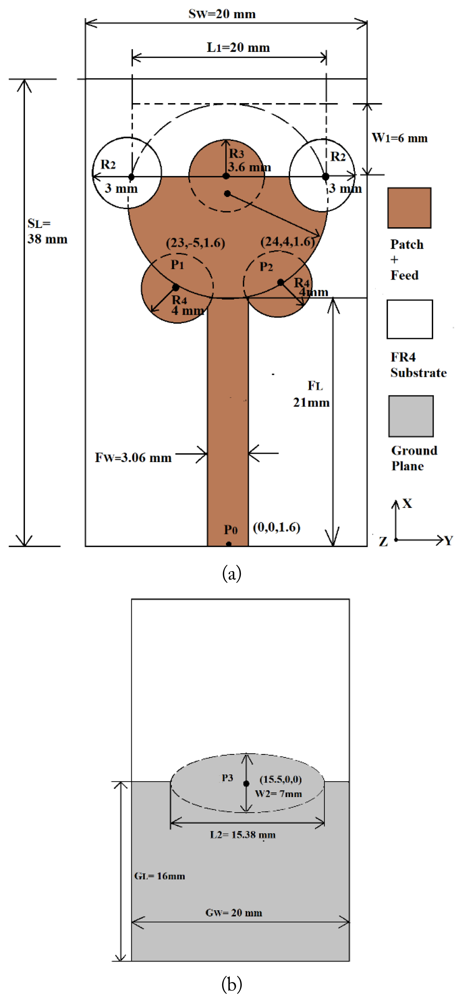
Geometry details of the proposed antenna: (a) top view of the radiating patch and (b) bottom view of the ground plane.
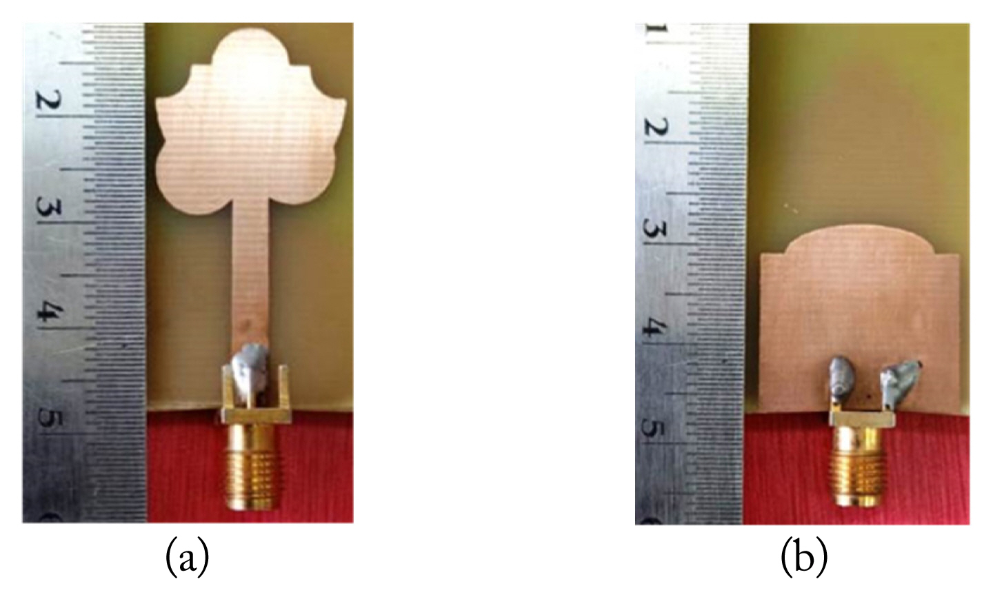
Fabricated snapshot of the proposed antenna: (a) top view and (b) bottom view.
The tree-like radiating patch (Fig. 1(a)) begins with a circular disk with a radius of 9 mm. The upper portion of the circular disk is etched so as to shape it as a semicircular patch. Two identical circular disks of a radius of 3 mm are removed from the top corner portion of the semicircular patch. Two identical circular patches of a radius of 4 mm are placed at two coordinate positions P1 and P2 of the patch, as shown in Fig. 1(a). The reference coordinate position is indicated as P0 (0, 0, 1.6), and the coordinate positions of the two circular patches are P1 (23, −5, 1.6) and P2 (24, 4, 1.6), as depicted in Fig. 1(a). Next, a patch (circular) of a radius 3.6 mm is added in the middle position to complete the radiating patch. A vase-shaped ground plane is shown in Fig. 1(b), which consists of a rectangular ground plane of length = 16 mm and width = 20 mm. An elliptical ground is added to the rectangular ground plane. The elliptical ground portion has dimensions of L2 = 15.38 mm and W2 = 7 mm; it is placed at the coordinate position of P3 (15.5, 5, 0) as shown in Fig. 1(b). The top and bottom views of the fabricated antenna are shown in Fig. 2.
III. Design Procedure
The four-stage detailed design procedure of the proposed antenna is illustrated in Fig. 3. The proposed antenna design procedure starts with a circular patch antenna. A rectangular slit of length L1 and width W1 is made on the initial circular patch, resulting in Antenna A. Furthermore, two circular slits of radius R2 are made on Antenna A, generating Antenna B. Next, a circular patch of radius R3 is inserted on the top edge of the semicircular patch, along with two circular patches of radius R4 at positions P1 and P2, resulting in Antenna C. Finally, an elliptical patch with a major axis of 3 mm and ratio of 2.5 is added on the top edge of the partial ground plane of Antenna C, generating the proposed antenna design (Antenna D).
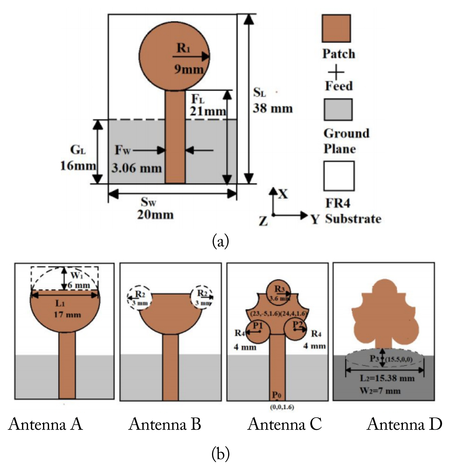
(a) Initial circular patch antenna and (b) four-stage design procedure of the proposed antenna.
A comparison of the S11 versus frequency responses of all the antenna designs discussed in the four-stage antenna design procedure is given in Fig. 4. Fig. 4 shows that the proposed antenna (Antenna D) offers the widest impedance bandwidth compared with the other intermediate antenna designs.
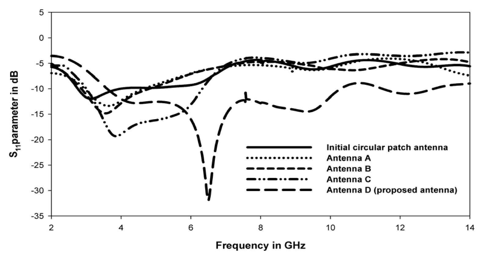
Simulated S11 versus the frequency responses of all antenna designs discussed in the four-stage antenna design procedure.
IV. Parametric Study
A detailed parametric study on the key design parameters has been carried out to understand the effect of each parameter on antenna performance.
The parametric study is conducted on the radius of the initial circular patch antenna (R1), where R1 is varies from 7 mm to 10 mm with an increment of 1 mm. The S11 and gain versus frequency responses corresponding to the variation of R1 are given in Fig. 5. From the S11 versus frequency plot, the impedance bandwidth of the antenna increases with an increase of R1. However, from the gain versus frequency plot, the antenna gain decreases as R1 increases. Considering both the impedance bandwidth and gain, R1 = 9 mm is considered the optimal value to implement the proposed antenna.
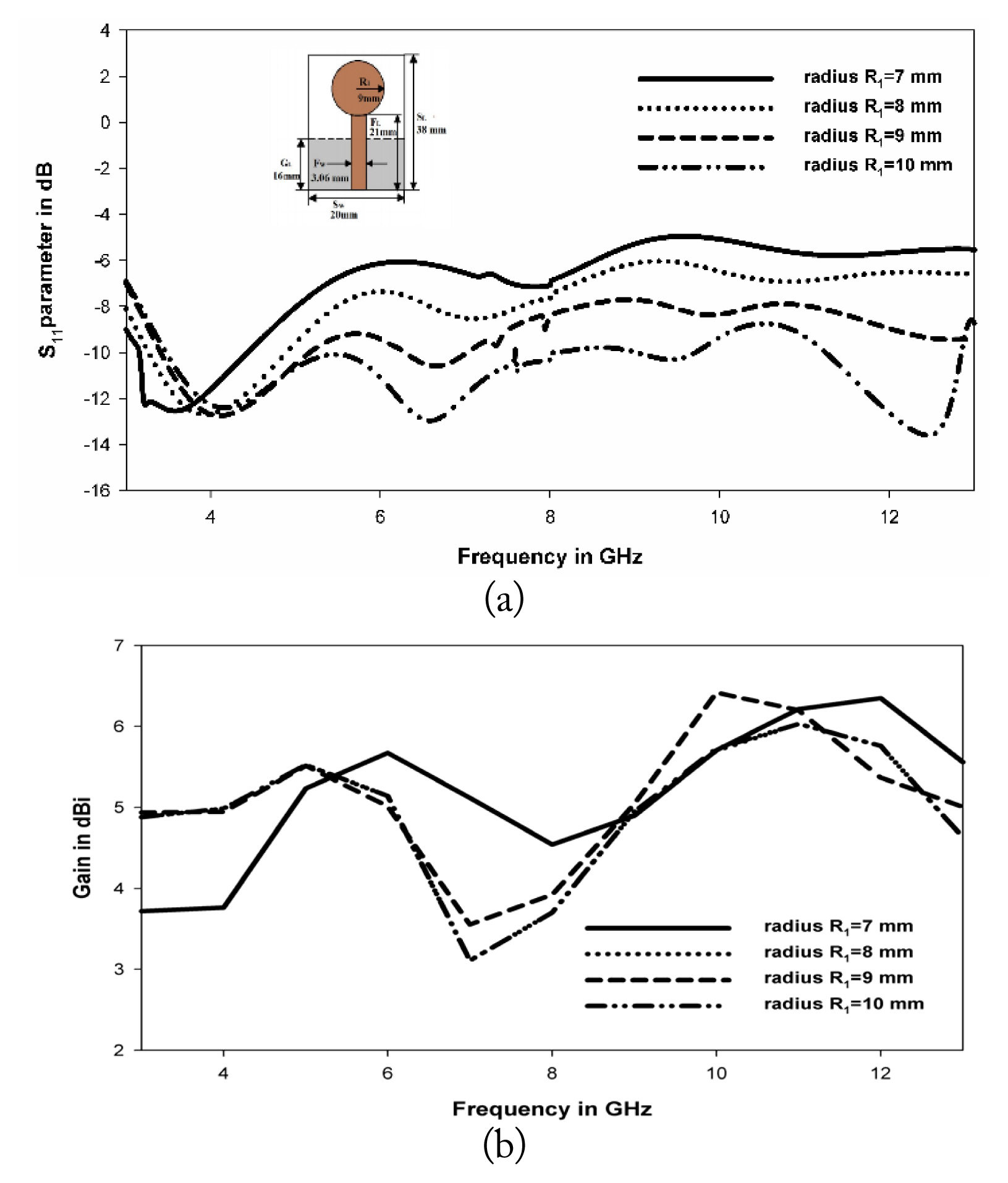
Simulated (a) S11 versus frequency and (b) gain versus frequency response corresponding to the variation in R1.
Next, the width of the rectangular slit (W1) made on the initial circular patch varies from 3 mm to 8 mm, with an increment of 1 mm. The S11 and gain versus frequency response corresponding to the variation of W1 is shown in Fig. 6. From the S11 versus frequency plot, the impedance bandwidth of the antenna increases with an increase of W1. However, from the gain versus frequency plot, the antenna gain decreases as W1 increases. Considering both impedance bandwidths and gain, W1 = 6 mm is considered the optimal value to implement the proposed antenna.
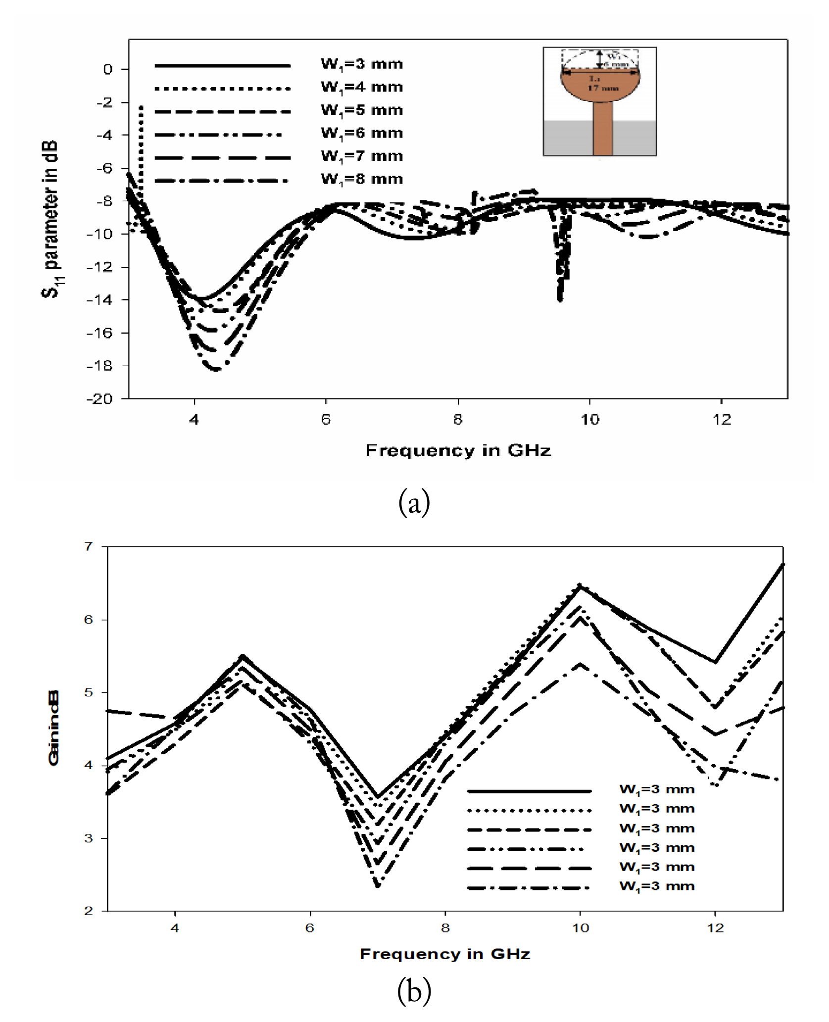
Simulated (a) S11 versus frequency and (b) gain versus frequency response corresponding to the variation in W1.
Next, the radius of the two circular slits (R2) of Antenna B varies from 1 mm to 5 mm, with an increment of 1 mm. The S11 and gain versus frequency responses corresponding to the variation of R2 are shown in Fig. 7. From the S11 versus frequency plot, the impedance bandwidth of the antenna increases with an increase in R2. However, from the gain versus frequency plot, the antenna gain decreases as R2 increases. Considering both the impedance bandwidth and gain, R2 = 3 mm is considered the optimal value to implement the proposed antenna.
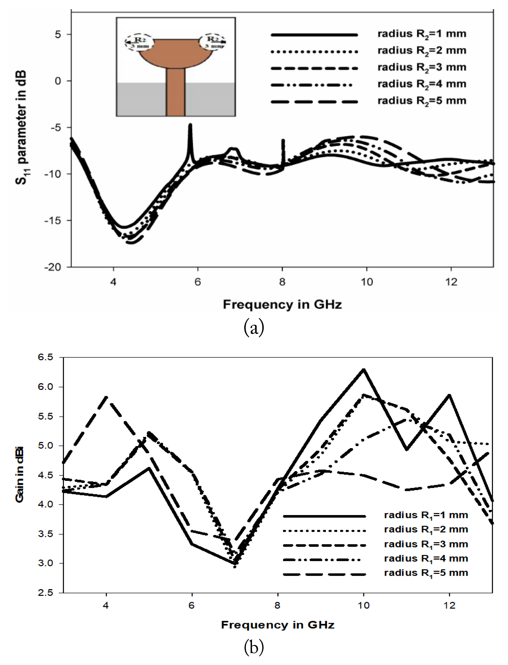
Simulated (a) S11 versus frequency and (b) gain versus frequency response corresponding to the variation in R2.
Next, the parametric variation of the radius (R3) of the circular patch inserted on the top edge of the semicircular patch and radius (R4) of the two circular patches at positions P1 and P2 of Antenna C is studied simultaneously. R3 varies from 1.6 mm to 3.6 mm, and R4 varies from 2 mm to 4 mm, both with an increment of 1 mm, respectively. The S11 and gain versus frequency responses corresponding to the variation of R3 and R4 are shown in Fig. 8. From the S11 and gain versus frequency plots, both the impedance bandwidth and gain of the antenna increase with an increase in R3 and R4. Considering both the impedance bandwidth and gain, R3 = 3.6 mm and R4 = 4 mm are considered the optimal values to implement the proposed antenna.
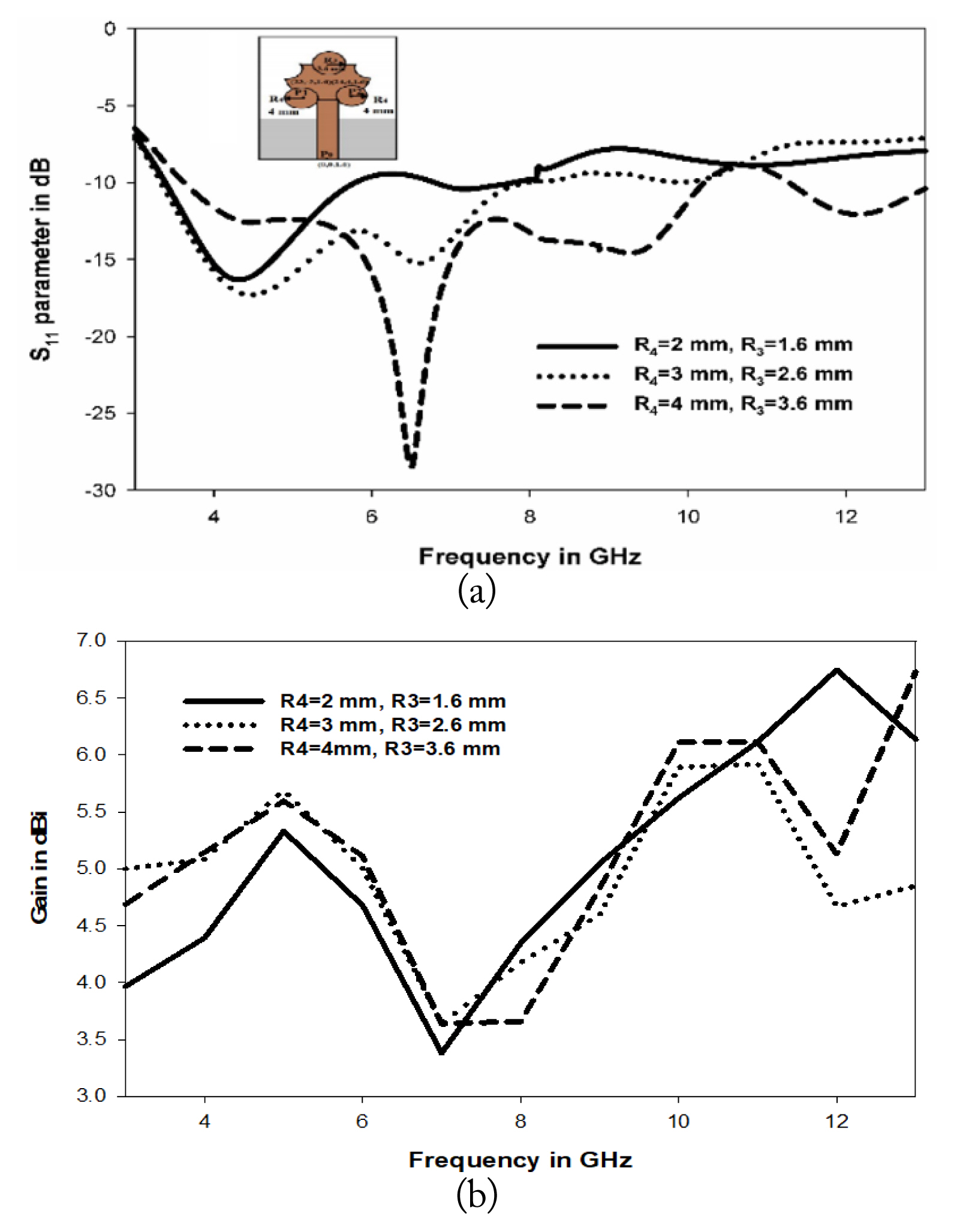
Simulated (a) S11 versus frequency and (b) gain versus frequency response corresponding to the variations in R3 and R4.
Furthermore, the parametric variation of the ground plane length (GL) is also studied. GL varies from 14 mm to 17 mm, with an increment of 1 mm. The S11 and gain versus frequency responses corresponding to the variation of GL are shown in Fig. 9. From the S11 and gain versus frequency plots, both the impedance bandwidth and gain of the antenna increase with an increase in GL. Considering both the impedance bandwidth and gain, GL = 16 mm is considered the optimal value to implement the proposed antenna.
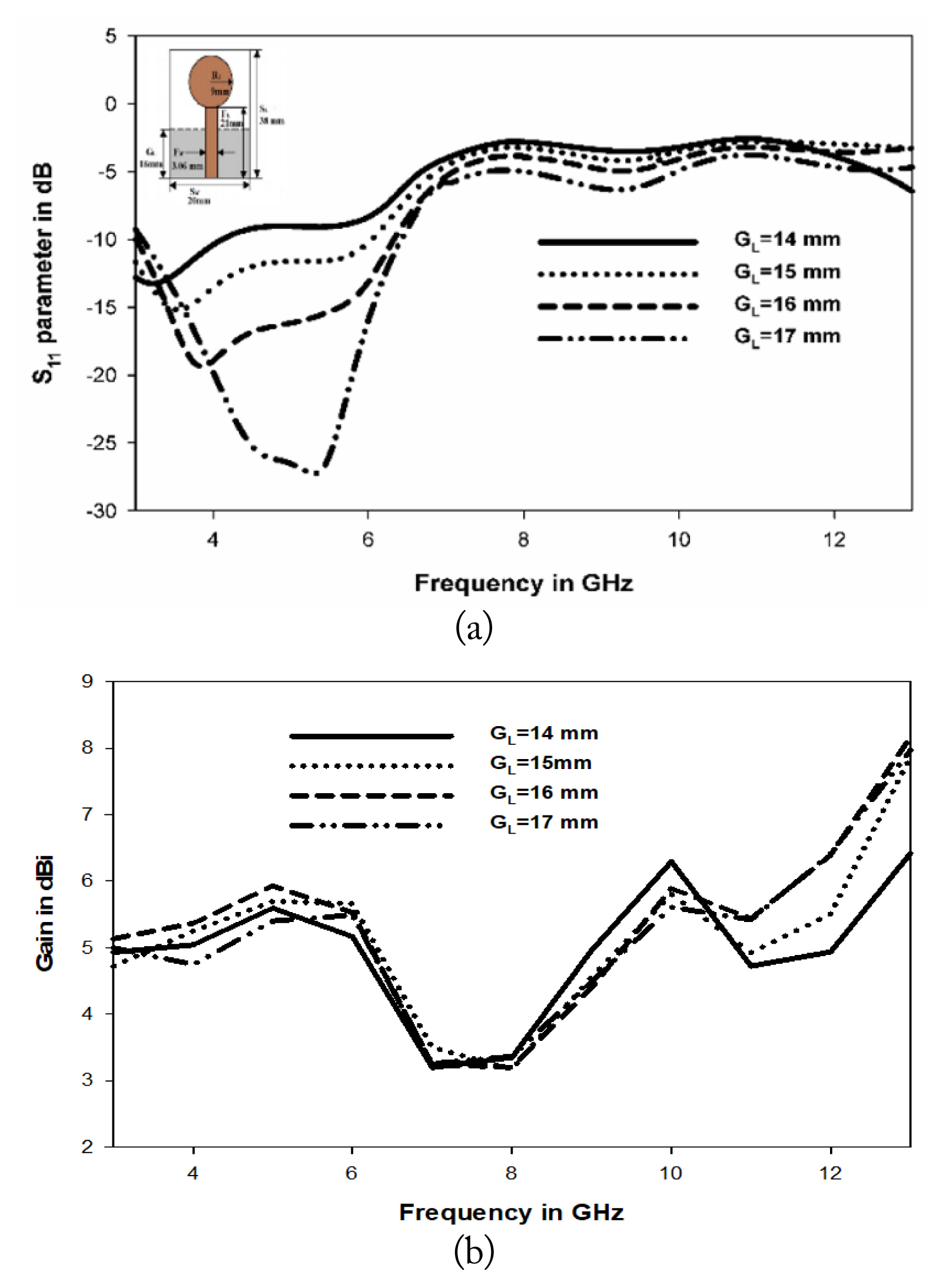
Simulated (a) S11 versus frequency and (b) gain versus frequency response corresponding to the variation in GL.
Finally, a parametric study of the different dimensions of the elliptical patch inserted on the top edge of the ground plane is also conducted. The major axis and ratio of the elliptical patch vary from 2 mm to 3 mm and 1.5 to 2.5, respectively, with an increment of 0.5 mm. The S11 and gain versus frequency responses corresponding to the variation of different dimensions of the elliptical patch are shown in Fig. 10. From the S11 and gain versus frequency plots, both the impedance bandwidth and gain of the antenna increase with an increase in the different dimensions of the elliptical patch. Considering both the impedance bandwidth and gain, major axis of 3 mm and ratio of 2.5 are considered the optimal values of the elliptical patch for implementing the proposed antenna.
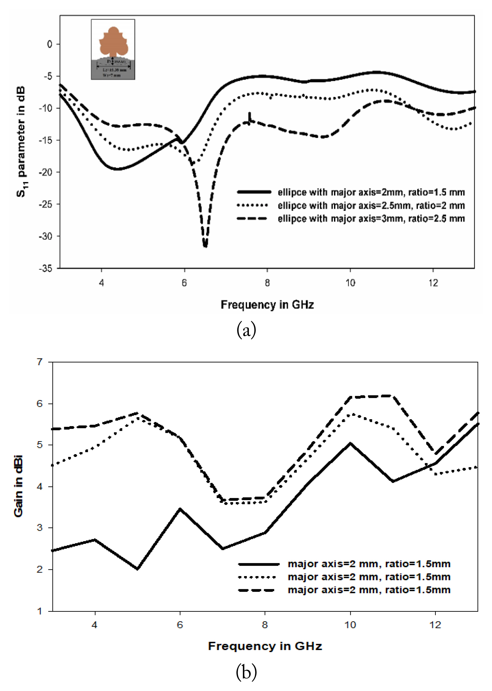
Simulated (a) S11 versus frequency and (b) gain versus frequency response corresponding to the variations of the different dimensions of the elliptical patch inserted on the ground plane.
V. Results and Discussion
In this section, the simulated and tested results (Fig. 11) of the proposed antenna are discussed. The measured S11 parameter is examined using the R&S ZNB20 vector network analyzer (Rohde & Schwarz, Munich, Germany). The 9.4 GHz (3.6–13 GHz) bandwidth is obtained by simulating the proposed antenna using the HFSS software simulation tool, which provides a simulated resonant frequency of 6.5 GHz and percentage bandwidth of 144.62%.

S11 parameter plot for the proposed antenna.
The results show a 9.3-GHz bandwidth for the proposed antenna. The bandwidth ranges from 3.8 GHz to 13.1 GHz, providing a percentage bandwidth of 136.76%. The resonant frequency occurs at 6.8 GHz. Using three intermediate stages, the proposed antenna provides 9.4 GHz broadband ranges from 3.6 GHz to 13 GHz.
The gain versus frequency plot is shown in Fig. 12. A peak gain of 6.5 dBi (measured) is achieved at 10 GHz. The radiation efficiency of the proposed antenna is measured at three distinct frequencies of 6.8 GHz, 7.3 GHz, and 8 GHz. Here, 73.46%, 77.51%, and 68.11% of measured radiation efficiencies are obtained at 6.8 GHz, 7.3 GHz, and 8 GHz respectively.
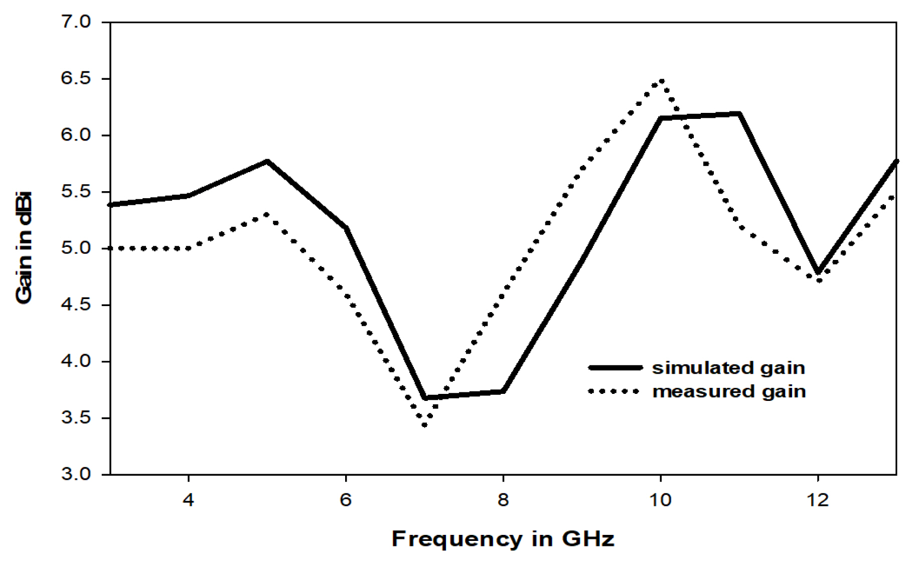
Gain plot of the proposed antenna.
The normalized radiation patterns (Φ = 0° plane and Φ = 90° plane) of the proposed antenna appear in Fig. 13(a)–(c), giving monopole-type radiation patterns in both the Φ = 0° plane and Φ = 90° plane.

Radiation patterns (Φ = 0° and 90° plane) of the proposed antenna at (a) 6.8 GHz, (b) 7.3 GHz, and (c) 8 GHz.
In the case of the initial circular patch antenna, only the 0.25 GHz (3.75–4.0 GHz) bandwidth has been obtained. Using three intermediate stages, the proposed antenna provides a 9.4 GHz (simulated) bandwidth ranging from 3.6 GHz to 13 GHz. Much more bandwidth has been obtained from the proposed design.
VI. Performance Comparison
The performance of the proposed antenna is compared with other antennas in the literature based on the electrical dimension, bandwidth, peak gain, efficiency, and fractional bandwidth of the antenna. The results are listed in Table 1. Table 1 shows that regarding the bandwidth and gain, the designed antenna provides the best performance. Here, λ0 is the free-space wavelength at the lower edge measured frequency of 3.8 GHz. In the proposed design, the main objective has been to design a broadband antenna with high gain, which makes the proposed design highly suitable for broadband applications.
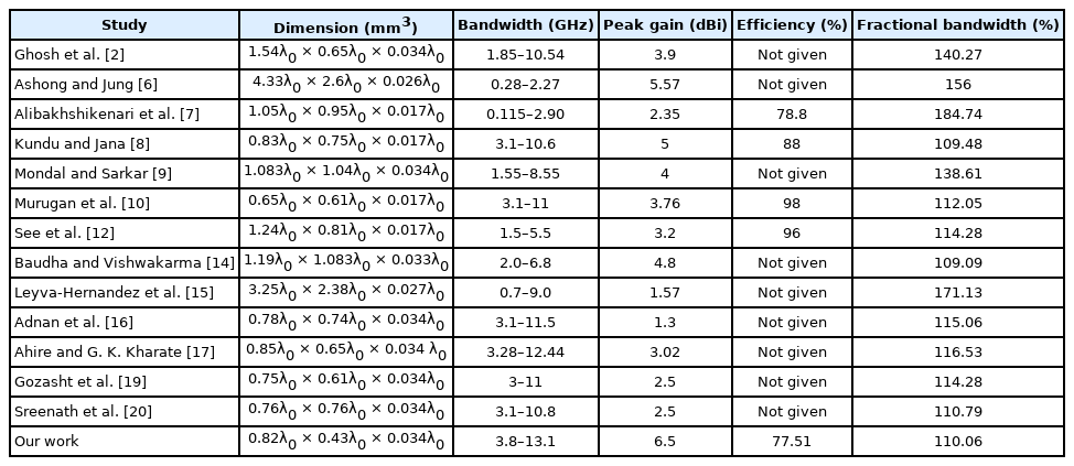
Performance comparison of the proposed antenna with other antennas in the literature
VII. Conclusion
A small monopole antenna is suggested. It provides broadband with good gains. The measurements have been performed on the fabricated antenna. The experimental results are in parity with the simulated results. The bandwidth, gain and radiation patterns of the fabricated antenna are found to be in parity with the simulated results.
References
Biography

Susmita Bala received her M.Tech. degree from Jadavpur University, West Bengal. She is presently filling in as an assistant professor at the Department of Electronics, Vidyasagar University. She is additionally working toward her Ph.D. at the Department of Engineering and Technological Studies, University of Kalyani. Her interested area incorporates microstrip antenna design for wireless communication systems.

P. Soni Reddy received a B.Tech. degree in ECE from WBUT, West Bengal, India, in 2011 and received her M.Tech. degree in ECE from KGEC, Kalyani, in 2016 under MAKUT, West Bengal. Since November 2017, she has been serving as a guest lecturer in the DETS, Kalyani University. Her research interests incorporate SIW coordinated MSA, reduced-size multiband defected ground structure antenna and miniaturized DRA. She is the beneficiary of university medal and received an award certificate for the third position in the University in M.Tech. degree assessment 2016 in ECE; she also ranked first in the specialization of Communication Engineering.

Rahul Mondal received a B.Tech. degree in EIE from DETS, Kalyani University, WB, India. He received a M.Tech. degree in CE in 2017. He was awarded first rank in the M.Tech examination. Since November 2017, he has been working as a Guest Lecturer in the Department of Engineering and Technological Studies (DETS), Kalyani University. His field of research incorporates FSS, MSA, and Rasorber. Presently, he is pursuing a Ph.D. (Tech.) degree at DETS, Kalyani University.

Partha Pratim Sarkar was awarded a Ph.D. degree in Engineering from Jadavpur University in 2002. He acquired his M.E. from Jadavpur University in 1994. He earned his B.E. degree in ETC from B.E. College, Calcutta University, in 1991. He is a professor at the Department of Engineering and Technological Studies, University of Kalyani. His interested research area incorporates microstrip antenna, microstrip filter, frequency selective surfaces, and artificial neural networks.

Sushanta Sarkar received his M.Tech. from Kalyani Govt. Engineering College in 2010. He earned his B.E. in ECE from Bengal Engineering and Science University, Shibpur in 2008. He received a Ph.D. from Department of Engineering and Technological Studies, Kalyani University in the year 2015. He is working as an assistant professor at the Department of Engineering and Technological Studies, Kalyani University. His research area is microstrip antenna design.