I. Introduction
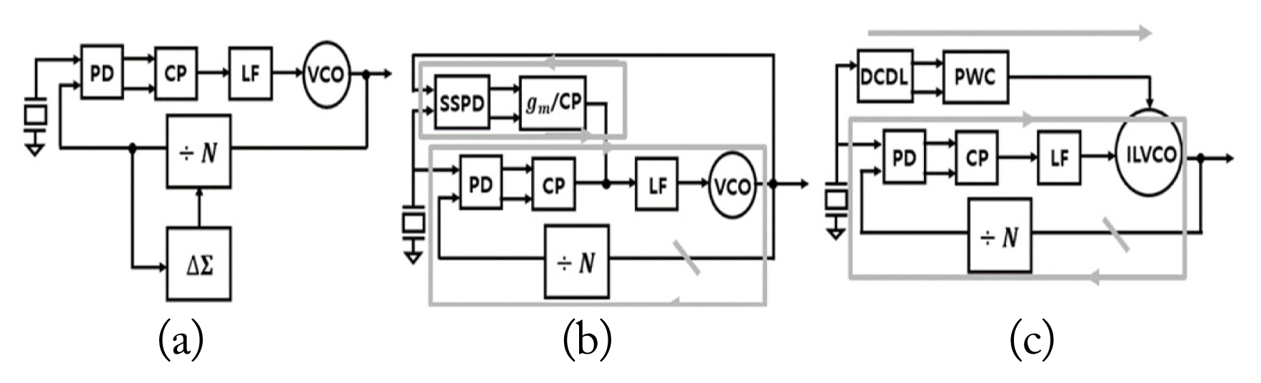
For the last decade, sub-sampling phase-locked loop (SSPLL) and injection-locked phase-locked loop (ILPLL) have been actively researched to suppress in-band phase noise by N2 when transferred to PLL outputs [1–4], where N is the division number in the feedback path in Fig. 1(a). However, applying SSPLL and ILPLL at the millimeter wave (mm-wave) causes some significant problems. Because sub-sampling phase detectors (SSPD in Fig. 1(b)) and pulse width controls (PWC in Fig. 1(c)) are directly connected to the voltage-controlled oscillator (VCO) and injection-locked VCO (ILVCO), they consume lots of power and cause series spurs.
Due to the low quality-factor of capacitors in mm-wave and CMOS (complementary metal-oxide-semiconductor) flicker noise, the phase noise of CMOS VCO is very poor and consumes a lot of power. Instead of running VCO at mm-wave, various combined structures of lower frequency SSPLL or ILPLL and following frequency multipliers have been preferred [5–9].
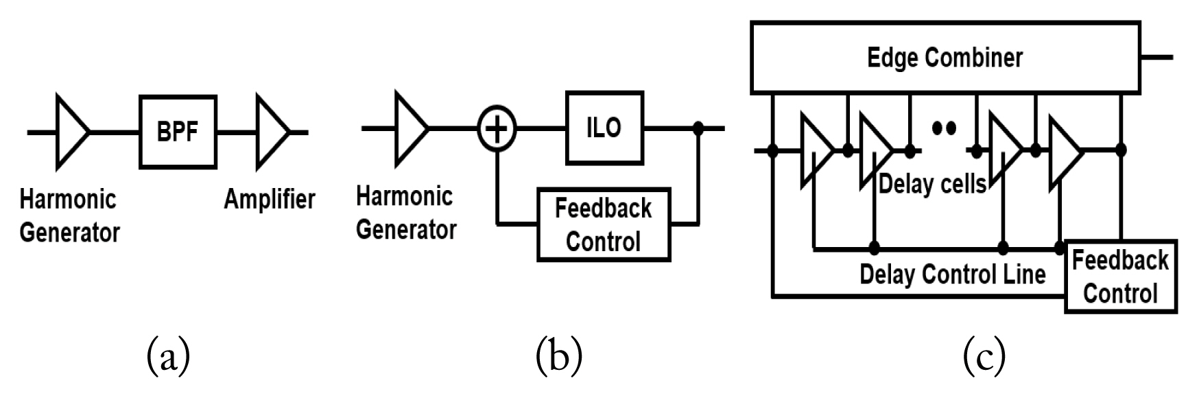
As shown in Fig. 2(a), a tuned-frequency multiplier (TFM) generally consists of a harmonic generator (HG), a band-pass filter (BPF), and an amplifier. Overdriving an amplifier generates weak higher harmonics of the fundamental tone and the desired harmonic is conserved by a simple BPF, such as a LC (inductor and capacitor) resonant tank. An additional LC-tuned amplifier is usually used to achieve a suitable amplitude to drive the next stage and suppress unwanted harmonics. While a TFM is the simplest frequency multiplier, it suffers from unwanted harmonics. Particularly, harmonic rejection of the fundamental tone is relatively poor [9]. A more efficient method of performing better harmonic suppression is to inject high harmonics into a free-running oscillator (Fig. 2(b)). An injection-locked frequency multiplier (ILFM) is able to suppress harmonics significantly by forcing oscillation at the desired harmonic, but it suffers from a limited injection-locking range, and additional error-correcting feedback circuitries are mostly required to secure a reliable operable frequency range [10]. A multi-phase-based topology (Fig. 2(c)) frequency multiplier can be considered a candidate [11], but output frequency accuracy directly depends on phase-shifting accuracy, which might shift due to PVT (process, power supply voltage, and temperature) variations without a phase-error correcting loop.
In this paper, we present a single-stage 12-times frequency multiplier which is based on TFM topology. To the best of our knowledge, no other published papers have achieved a more than 4-times mm-wave frequency multiplier using one stage; rather, they have used more than two cascade stages, such as 2-times plus 4-times, resulting in 8-times frequency multipliers. This paper’s ultimate goal is to provide an efficient mm-wave frequency multiplier solution for a 5G frequency synthesizer. This paper is organized as follows. In Section II, the proposed 12-times frequency multiplier structure is introduced. In addition, the methods of optimizing conversion gain variations and a harmonic rejection ratio (HRR) for the target frequency band are described. Section III shows the chip fabrication and measurement results. A comparison of this study with other recently published frequency multipliers is provided in Table 1 [11–14]. A summary and conclusion are reported in Section IV.
II. 12-Times Frequency Multiplier Design
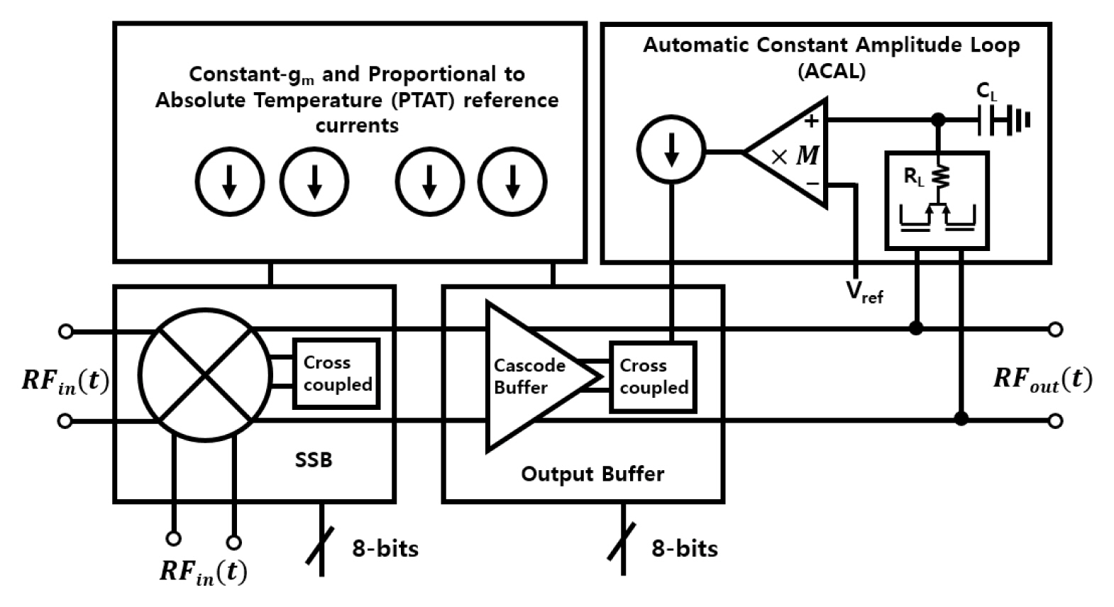
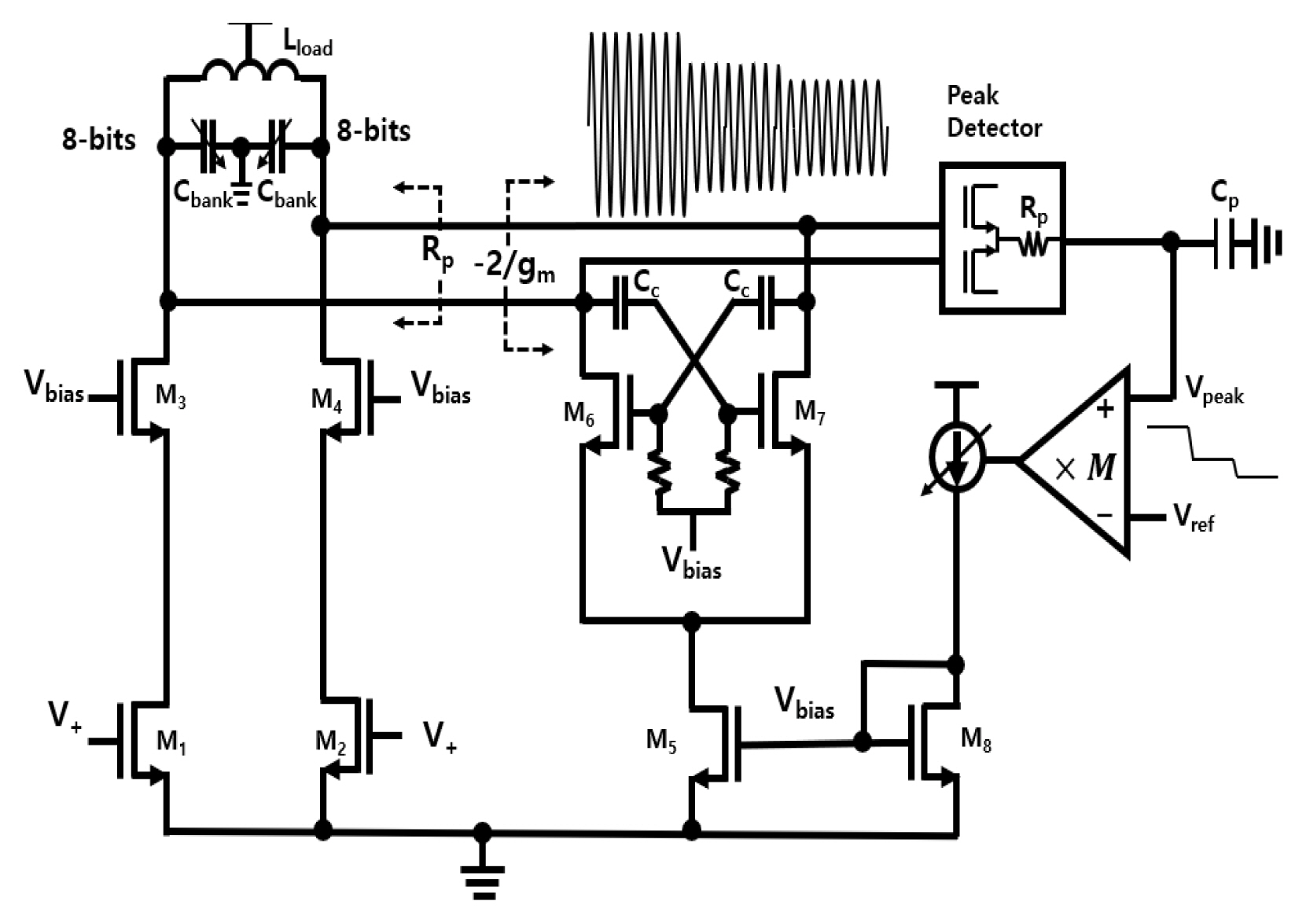
Fig. 3 shows the proposed 12-times frequency multiplier block diagram. It is composed of a modified double-balanced mixer (DBM)-type HG and a modified cascode buffer with constant-gm, proportional absolute temperature (PTAT) current references, and an automatic constant amplitude loop (ACAL).
1. Proposed 12-Times Harmonic Generator
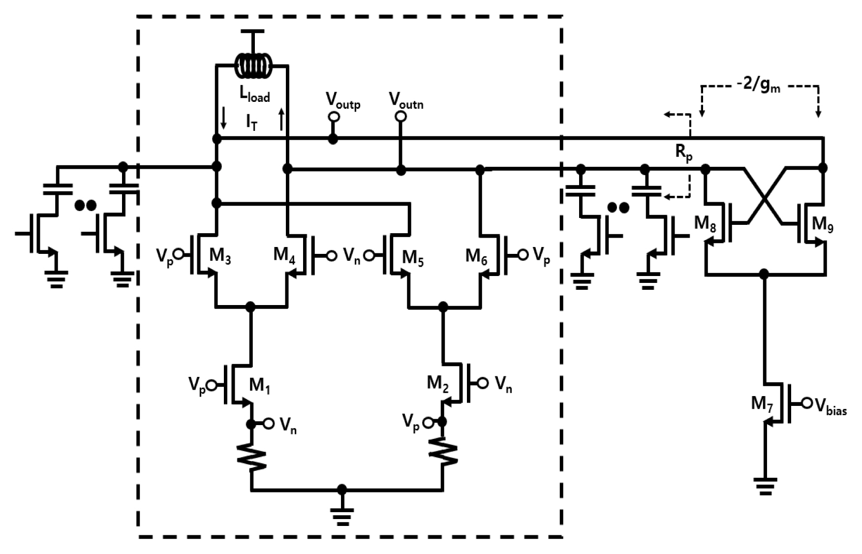
The detail circuit schematic of the proposed 12-times HG is shown in Fig. 4. The circuitries inside the dotted box are a modified DBM. If Vp – Vn is big enough to turn M1 – M6 on and off completely, the corresponding differential current, IT, can be expressed as
where IM1 – IM6 are bias currents when M1 – M6 are turned on. The differential currents of the top pairs are
The currents of M1 and M2 are
where Idc is the dc bias current, τ is the turn-on time, and T is the period of the applied first fundamental. Setting τ = T/24 in Eq. (3), Eq. (1) is re-arranged as
(4)
where β2 – β14 are the calculated current coefficients, the values of which are:
The current coefficient at the 12th harmonic is not dominant, but 20log (β4/β12) is only 2.3 dB, which can be easily overcome by the LC resonated at the 12th harmonic.
The output impedance is the LC bank, the states of which are controlled by 8 digital bits. The C bank is binary weighted as C8 = 2C7 = 22C6 = 23C5 = 24C4 = 25C3 = 26C2 = 27C1. As a result, the target frequency band from 16 GHz to 28 GHz is divided into 256 sub-frequency bands. The resonant frequency at each state can be represented as follows:
where Dk is the kth capacitor digital control bit, which is either 1 or 0,
D k ¯
where H = 2/(gmRp). For example, Req will be three times that of Rp when H = 1.5, with a smaller current for the added negative-gm pair than the IT required to maintain the output amplitude. The negative-gm is able to improve the HRR performance [10]. Parallel RLC impedance, ZRLC(ω), is expressed as
The HRR in dB, HRRdB(ω0 ± Δω), at Δω from the resonant frequency, ω0 is defined as the dB expression of the ratio of the impedance at ω0 and ω0 ± Δω, which can be derived as
where
2. The Buffer with Constant Output Amplitude Control
As shown in Fig. 6, we used the same cascode buffer topology in [10] to get more HRR and low power consumption, but we inserted a dc-blocking capacitor, Cc, for better power optimization, as shown in Fig. 6. By applying an appropriate Cc size, the load of the negative-gm pair can be reduced. So, there is room to increase the M6 and M7 device size to maintain the same load as before, which leads the corresponding transconductance, gm, to increase with the constant current, Itail, because the overdrive voltage, (Vgs – Vth), is decreased. The buffer is composed of a typical cascode buffer, a negative-gm pair, and an automatic amplitude control loop (AACL). Just like the proposed HG, the buffer output of the LC-bank resonant is programmed by 8 digital bits. The equivalent parallel of the LC-bank resistance can be also manipulated by the positive feedback pair transconductance, gm, as in Eq. (7).
For the buffer output, Vout, the peak is detected though the RF peak detector. The Vpeak is compared with the Vref. If Vpeak > Vref, VI is increased to reduce Iref. Consequently, Itail is decreased so the transconductance, gm, of the M6 and M7 pair results in the reduction of Req in Eq. (7), which is proportional to the output amplitude. Similarly, when Vpeak > Vref, the output amplitude is reduced. Therefore, the AACL is able to help to keep a constant amplitude within 1 dB for a 6 dB input and the mentioned PVT variations.
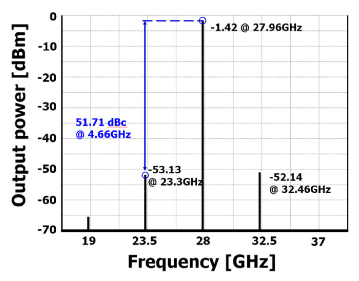
Fig. 7 shows the proposed 12-times frequency multiplier output power simulation when the output power is 1.42 dBm and the worst harmonic rejection is 51.71 dBc.
III. Fabrication and Measurement
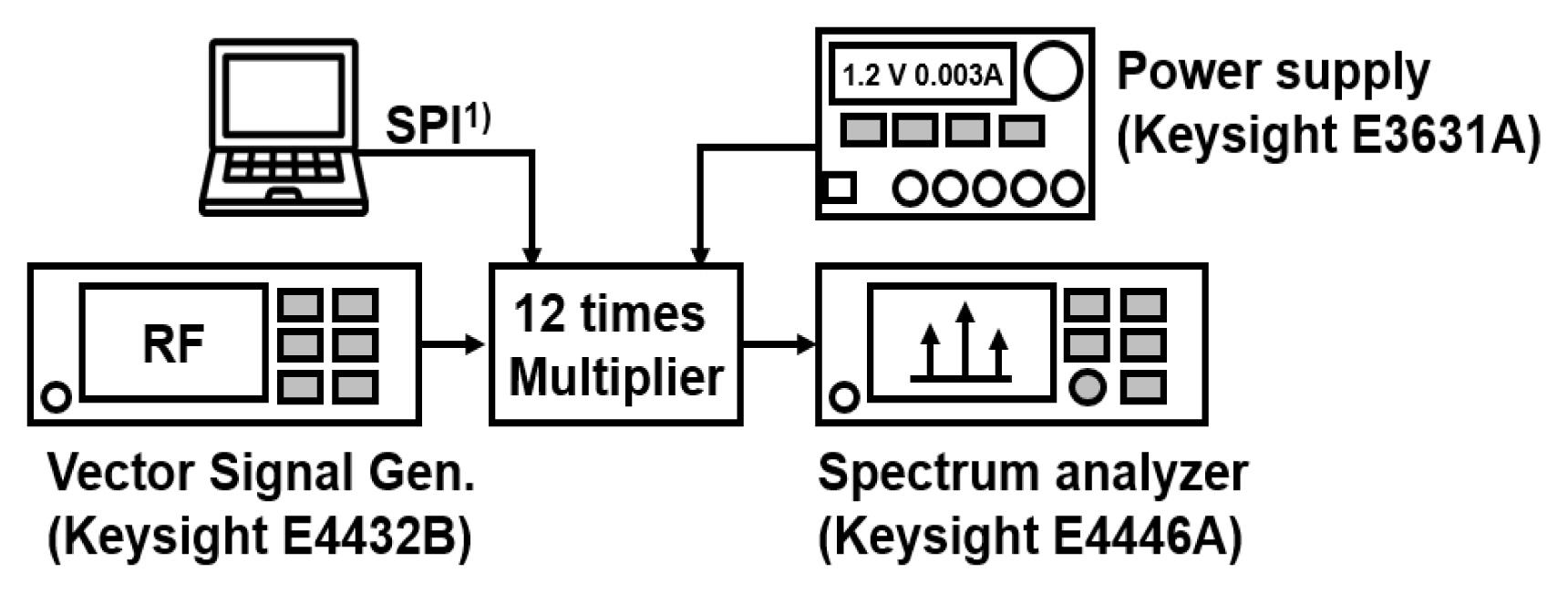
The prototype of the proposed 12-times frequency multiplier is fabricated on 65 nm CMOS technology and its size is 0.4 mm2, as shown in Fig. 8. The laboratory test environment is shown in Fig. 9.
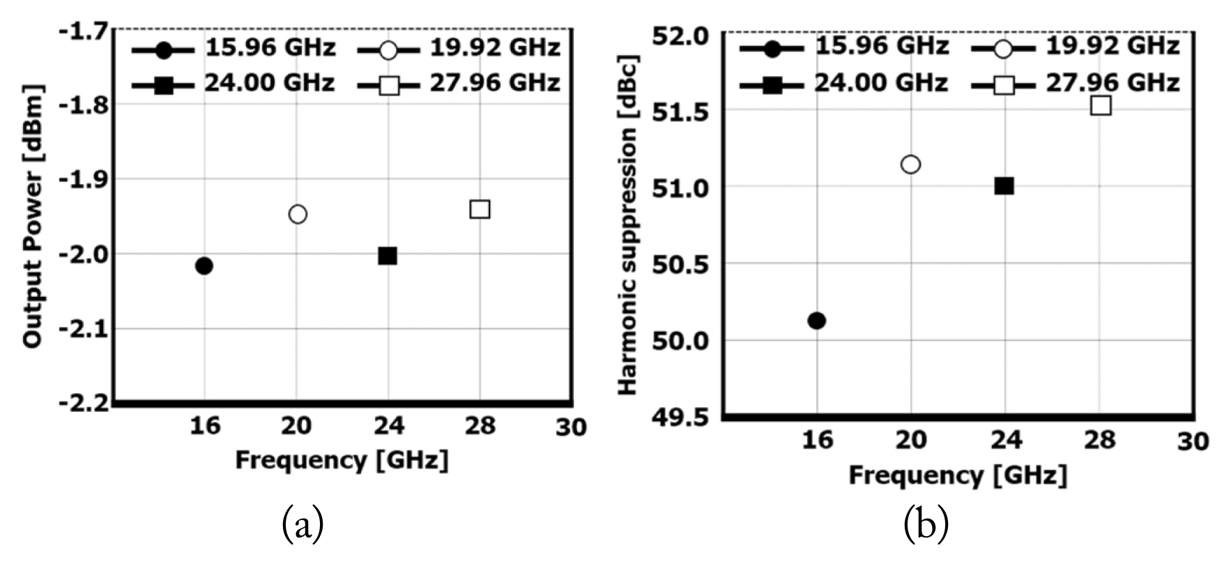
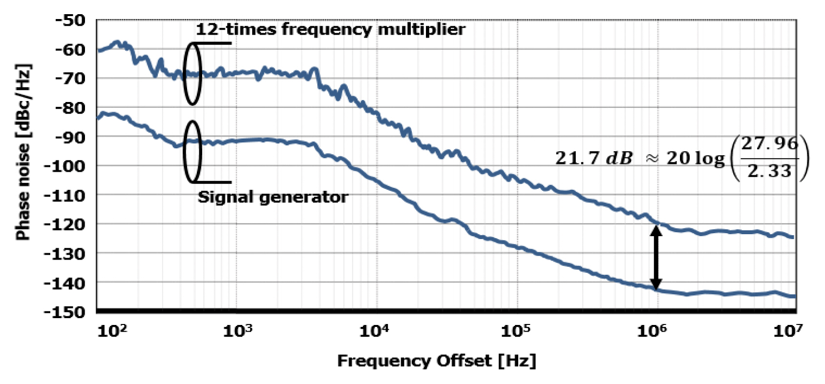
The harmonic measurements are shown in Fig. 10, where the worst harmonic rejection ratios are −50.1 dBc and −51.66 dBc on 15.96 GHz and 27.96 GHz, respectively. Fig. 11(a) shows the measurement of output power versus output frequency. The 12-times frequency multiplier output powers at 15.96 GHz and 27.96 GHz are −2.03 dBm and −1.94 dBm, respectively. The worst harmonic suppression versus output frequency is shown in Fig. 11(b), where the maximum harmonic suppression of the frequency multiplier is 51.5 dBc at 27.96 GHz. When compared with the simulation results, almost similar measurement results are obtained. The phase noise degradation due to the proposed multiplier is measured. As shown in Fig. 12, only 0.1 dB phase noise is added when compared with the mathematical phase noise degradation (20log (12) = 21.6 dB).
Table 1 presents a summary of recently published papers on mm-wave frequency multipliers, including the multiplier proposed in this paper. The proposed multiplier has better frequency range percent and power consumption performances. However, the multiplier used in [12] and [14] has a better harmonic rejection ratio because the proposed multiplier has a much bigger multiplication factor (12 vs. 3). To achieve a fair comparison, figure-of-merit (FoM) is calculated for each paper. The proposed multiplier achieves the best FoM among them.
The measurement results of the power consumptions for different frequencies and the output powers at different input powers when disabling AACL are summarized in Table 2.
IV. Summary and Conclusion
This paper proposed an unconventionally created frequency mm-wave HG based on a Gilbert cell DBM structure with a positive feedback pair. The nonlinear switching behaviors of a Gilbert cell’s top differential pair and bottom differential pairs create strong harmonics of double frequency of the fundamental tone. The consequent adjacent harmonics difference is twice the fundamental tone, which makes it easier to suppress unwanted harmonics. By adjusting a device’s turn-on time, τ, the current coefficient at the desired 12th harmonic can be improved. Furthermore, with the help of negative-gm, the proposed 12-times HG consumes only 4 mW. Since the HG is in the middle of a 5G synthesizer, one of 256 different frequency bands can be simultaneously programmed when the synthesizer frequency is digitally programmed. Consequently, a 54.5% frequency range is accomplished by 8-bit capacitor banks.
The cascode buffer proposed in this paper is able to suppress undesired harmonics further by applying an adequate current to a negative-gm pair and a PTAT reference current for each sub-frequency band to achieve more than 50 dBc harmonic rejection. Also, a newly adapted ACAL helps to reduce the output power variation to within 1 dB for PVT variation (±3σ process, ±10% power supply voltage, and temperature from −20°C to 100°C).