Design of a Wideband Printed Patch Dipole Antenna with a Balanced On-Board Feeding Network
Article information
Abstract
This paper proposes a wideband printed patch dipole antenna with a simple on-board feeding network. The proposed antenna is composed of two dipole radiators, a transmission line, and an on-board feeding network with a chip balun. The dipole radiators are printed on a substrate, and the edges of the radiators are truncated to create a hexagonal shape with wide impedance-matching characteristics. The chip balun is embedded in an RO4003C printed circuit board (PCB) to excite differential feeding to each radiator with a 180° phase difference. The proposed antenna is optimized using a CST Studio full electromagnetic software tool, and it is fabricated and measured in an anechoic chamber. The measured fractional bandwidth for the reflection coefficient below −10 dB is 79.5%, and the proposed antenna has a measured gain of 7.1 dBi at 3.5 GHz.
I. Introduction
Dipole antennas have been widely used for various applications, including wireless communication systems, radar systems, and localization systems [1–6]. Recent developments in system design technologies have led such systems to become small in platform size and to include multiple functions, such that the systems have required a wide operating frequency band, high integration, size miniaturization, and high radiation performance. In particular, the wide impedance-matching characteristics of dipole antennas are essential for operating multifunctional systems, and their directive radiation patterns are important for stably maintaining point-to-point communication links. To obtain wideband characteristics, 3D dipole antennas have been investigated using a biconical structure [7, 8], an additional parasitic element [9], and an indirect feeding structure [10]. However, these studies have difficulties with high integration into systems due to the bulky structure size and nondirective radiation patterns. To overcome these problems, printed patch dipole antennas for directive patterns have been introduced by employing various shapes, such as an ellipse, a bow tie, and a polygon [11–13]. Although such antennas can achieve wideband characteristics with stable boresight gains, it is essential that additional bulky baluns are elaborately designed for differential feeding to excite each radiator with a 180° phase difference [14]. To account for the additional baluns, research on using a small chip balun has been conducted to achieve size reduction of the differential feeding structure [15, 16]. However, their matching bandwidth is still narrow, lower than 10%, and an in-depth study is needed to analyze patch dipole antennas with integrated circuit baluns.
In this paper, we propose a wideband printed patch dipole antenna with a simple on-board feeding network. The proposed antenna is composed of two dipole radiators, a transmission line, and an on-board feeding network with a chip balun. The dipole radiators are printed on a substrate, and the edges of the radiators in the center of the substrate are truncated to create a hexagonal shape for direct connection with the transmission line and for wide impedance-matching characteristics. In addition, the transmission line is designed to operate as a quarter-wave transformer for impedance matching between the dipole radiators and the chip balun. The chip balun is embedded in an RO4003C printed circuit board (PCB) to excite differential feeding to each radiator with a 180° phase difference. This chip balun, which can reduce the size of the feeding network structure, is fed by a microstrip line and an SMA connector. The proposed antenna, including the chip balun circuit, is optimized using the CST Microwave Studio software tool [17]. To verify its feasibility, the proposed antenna is fabricated, and its antenna properties, such as reflection coefficients, radiation patterns, and gains, are measured in a full anechoic chamber. For antenna analysis, an equivalent circuit of the proposed antenna is modeled to analyze its impedance characteristics, and parametric studies are conducted to achieve wide-bandwidth characteristics.
II. Proposed Antenna Design and Measurement
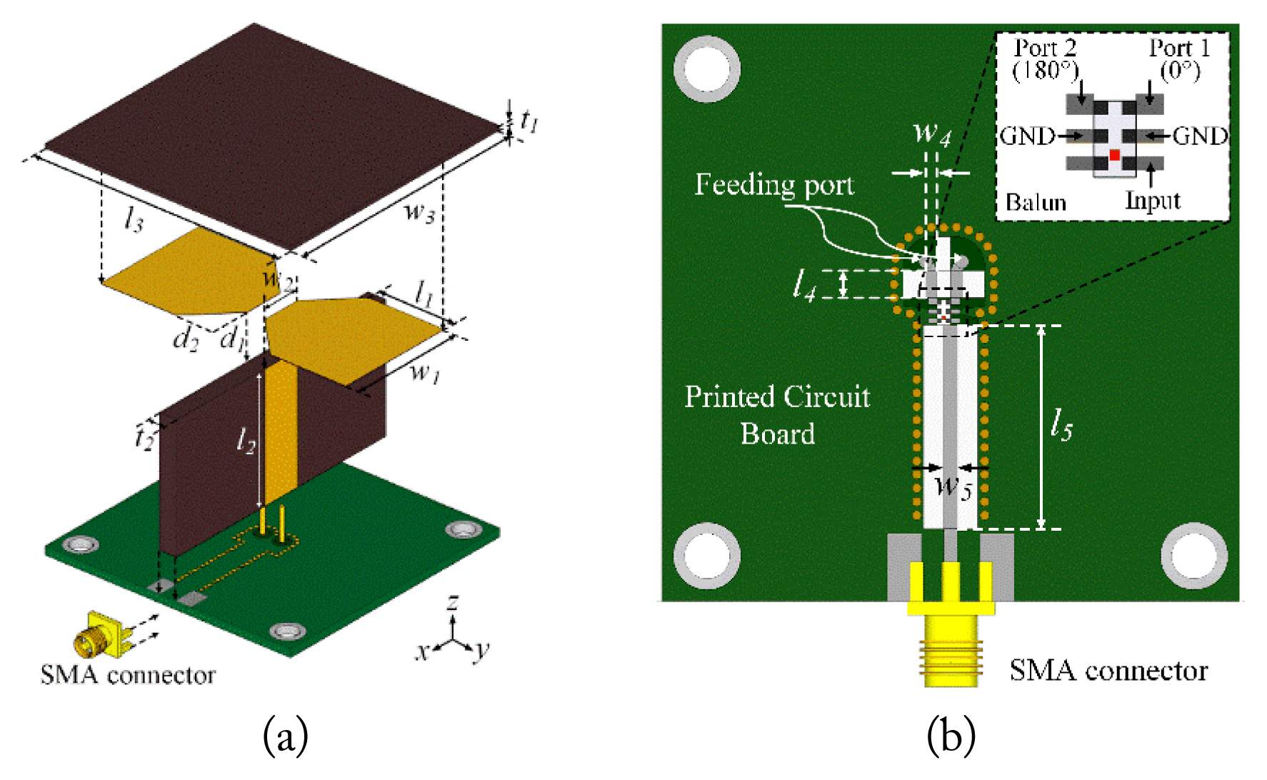
Fig. 1 shows the geometry of the proposed antenna composed of two dipole patch radiators, a parallel plate transmission line, and a feeding network with a chip balun. The patch dipole antenna is printed on a TLY-5 substrate (ɛr = 2.2, tanδ = 0.0009) having dimensions w3 × l3 × t1 (width × length × thickness). The dipole patches have a length l1 that can determine the resonant frequency, and its width w1 can enhance the impedance-matching characteristics at the resonant frequency. To achieve wideband characteristics, the radiator edges in the center of the substrate are truncated by width d1 and length d2. Note that a half-wavelength dipole antenna length generally has a single operating frequency with a narrow bandwidth [18], while a patch dipole can achieve a wideband characteristic by changing the width and length of the radiator, allowing a different current path for each operating frequency [19]. Thus, the geometry of the radiators becomes hexagonal, which can directly connect to the transmission line. In addition, the wide impedance-matching characteristics can be further improved by adjusting the slope of the truncated part for the radiators. The parallel plate transmission line printed on the TLY-5 substrate has a width w2 and a length l2. This transmission line is perpendicularly connected to the truncated part of the dipole radiators having a gap t2. In particular, l2 can be operated as a quarter-wave transformer to match the impedance between the dipole radiators and the chip balun. The feeding network is designed using an RO4003C (ɛr = 3.35, tanδ = 0.0027) PCB with a chip balun and differential microstrip lines to substitute for the bulky and complicated microstrip balun. The differential feeding lines having a length l4 and a width w4 are designed to have a line impedance of 100 Ω, and they are connected to each radiator by two via pins for a 180° phase difference excitation. An SMA connector is used to excite a signal for the chip balun through the microstrip line with width w5 and length l5.
The proposed antenna is optimized using a CST Studio full electromagnetic (EM) software tool including 3D EM modeling and a circuit schematic, which are sequentially simulated to obtain the impedance characteristics of the antenna and the PCB feeding network. The antenna radiators and the parallel transmission lines of the proposed antenna are simulated by 3D EM modeling of the structures. The PCB feeding network is designed based on a schematic layout, including the chip balun S-parameter, the microstrip feeding line, and the microstrip differential lines. Through the sequential simulations, the optimized design parameters and values are listed in Table 1.
Fig. 2 presents photographs of the fabricated antenna consisting of the dipole radiators, the transmission line, and the chip balun embedded in the PCB feeding network. It is essential to use a chip balun operating in a wide frequency band that incorporates the dipole radiator to achieve wideband characteristics. Thus, we employ the Johanson Technology chip balun (balanced impedance of 100 Ω from 2.8 to 6 GHz) [20] to excite differential feeding with a 180° phase difference to each dipole radiator. To verify its feasibility, the fabricated antenna is measured in a full anechoic chamber to observe antenna performances, such as reflection coefficients, gains, and radiation patterns.

Configuration of the fabricated antenna: (a) dipole radiators and parallel plate transmission line, (b) PCB feeding network, (c) assembled antenna.
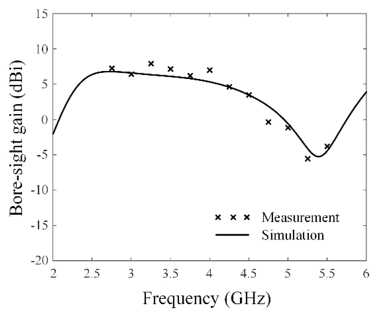
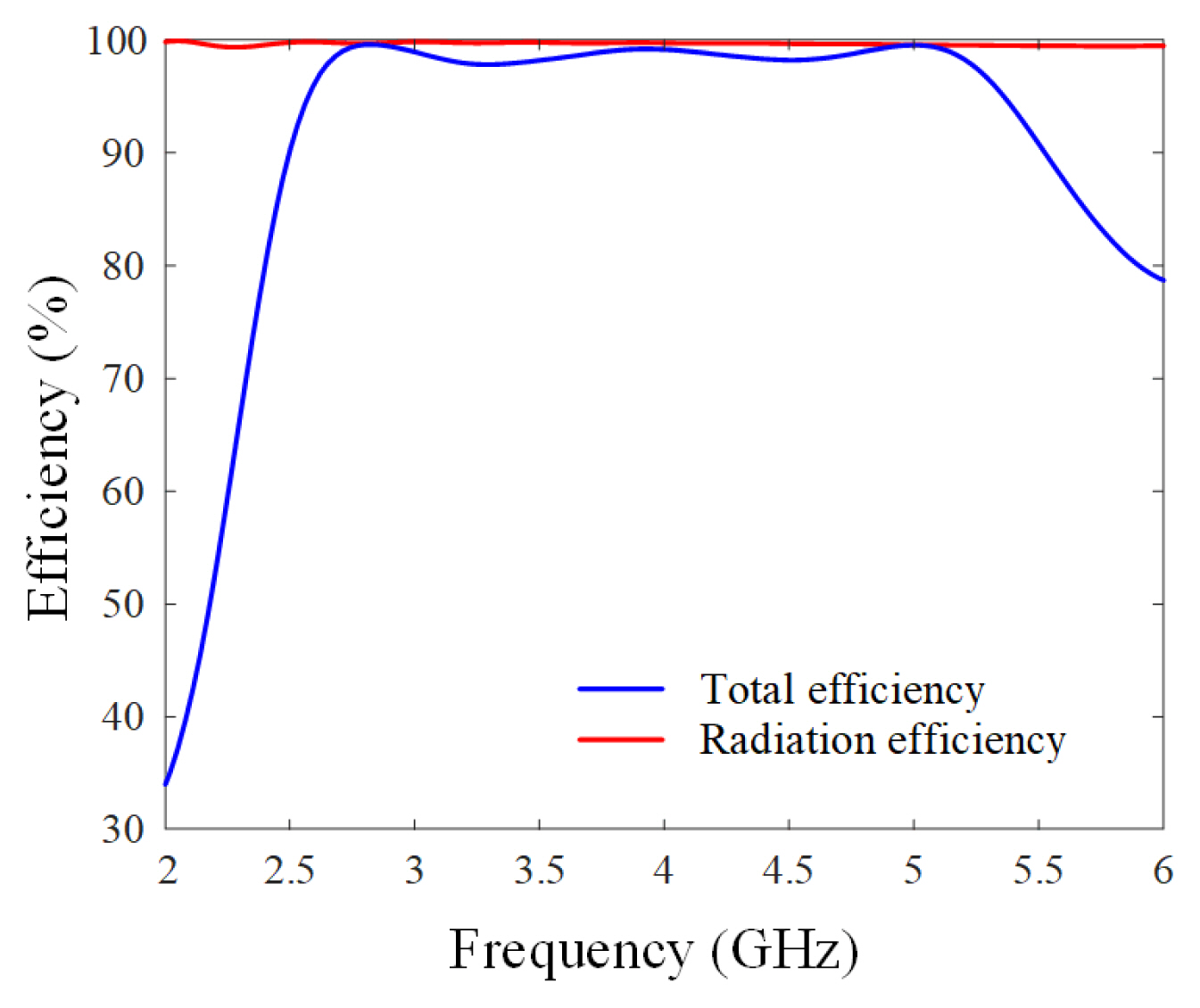
Fig. 3 represents the reflection coefficients of the proposed antenna; solid and dashed lines indicate the measured and simulated results, respectively. The measured and simulated reflection coefficients are below −10.5 dB and −11 dB, respectively, in the frequency range from 2.7 to 5.8 GHz. The measured and simulated fractional bandwidths at the center frequency of 4 GHz are 79.5% and 83.4%, respectively. Fig. 4 shows the boresight gains of the proposed antenna according to frequency. The solid line and the “×” markers indicate the simulations and measurements, respectively. Both simulated and measured gains are over 3 dBi in the frequency range from 2.75 to 4.5 GHz. Fig. 5 illustrates the measured and simulated 2D radiation patterns of the proposed antenna in the zx- and zy-planes at 3.5, 4.5, and 5.5 GHz. The measured cross-polarization levels at the boresight direction are lower than −17.5 dBi and −13.2 dBi in the zx- and zy-planes, respectively, at 3.5 GHz. The measured results agree well with the simulations. The measured half-power beam-widths (HPBWs) are 107° and 86° in the zx- and zy-planes at 3.5 GHz, and those at 4.5 GHz are 154° and 94°, respectively. Fig. 6 presents the total efficiency and the radiation efficiency according to frequency. The total efficiency of the proposed antenna considering the mismatch efficiency with frequency is simulated. The total efficiency is over 82% in the operating frequency range from 2.75 to 5.8 GHz, and it is 90.8% at 5.5 GHz. The radiation efficiency value is obtained as more than 98.3% across the whole operating frequency range.
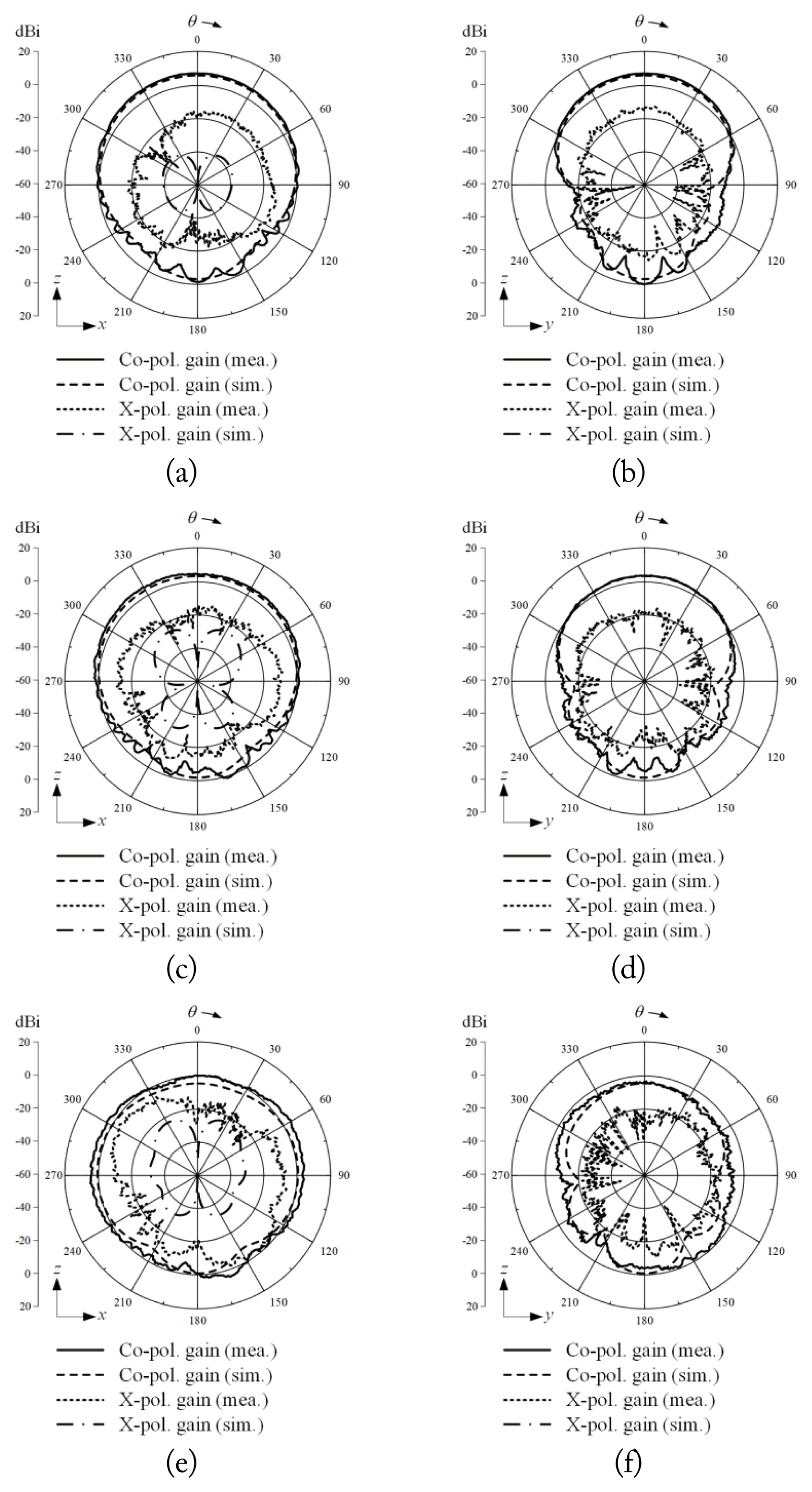
Simulated and measured 2D radiation patterns of the proposed antenna: (a) zx-plane at 3.5 GHz, (b) zy-plane at 3.5 GHz, (c) zx-plane at 4.5 GHz, (d) zy-plane at 4.5 GHz, (e) zx-plane at 5.5 GHz, (f) zy-plane at 5.5 GHz.
The results demonstrate that the proposed antenna can achieve wideband impedance characteristics and maintain stable gain performance using an on-board balanced chip balun for a simple feeding network. The antenna performances including fractional bandwidth, gain at the center frequency, integrated balun type, and antenna size are listed in Table 2 for comparison with previous studies. The proposed antenna can reduce the antenna size by less than 63% compared with antennas that use Guanella and microstrip line baluns, which have a length and width greater than one wavelength. In addition, the dipole in our study can enhance the impedance-matching bandwidth by more than 79% compared with previous studies that integrated chip baluns.
III. Analysis
To analyze the proposed antenna, an equivalent circuit is modeled, taking into account important antenna parts: the patch radiator, the transmission line, the chip balun, and the feeding port. Fig. 7(a) shows an equivalent circuit model of the proposed antenna including the transmission line, the chip balun, and the antenna resonant circuits to observe the input impedance characteristics. In the circuit model, the SMA port of 50 Ω is modeled as an inductance Lf to excite the 1:2 chip balun with a balanced impedance of 100 Ω. Through the chip balun, the parallel transmission line of the proposed antenna is connected to the parallel RLC element with R1, L1, and Cl representing the resonance of the dipole radiator. In particular, the parallel plate transmission line is operated as a quarter-wave transformer, and its characteristic impedance can be obtained using an equation as follows [21]:
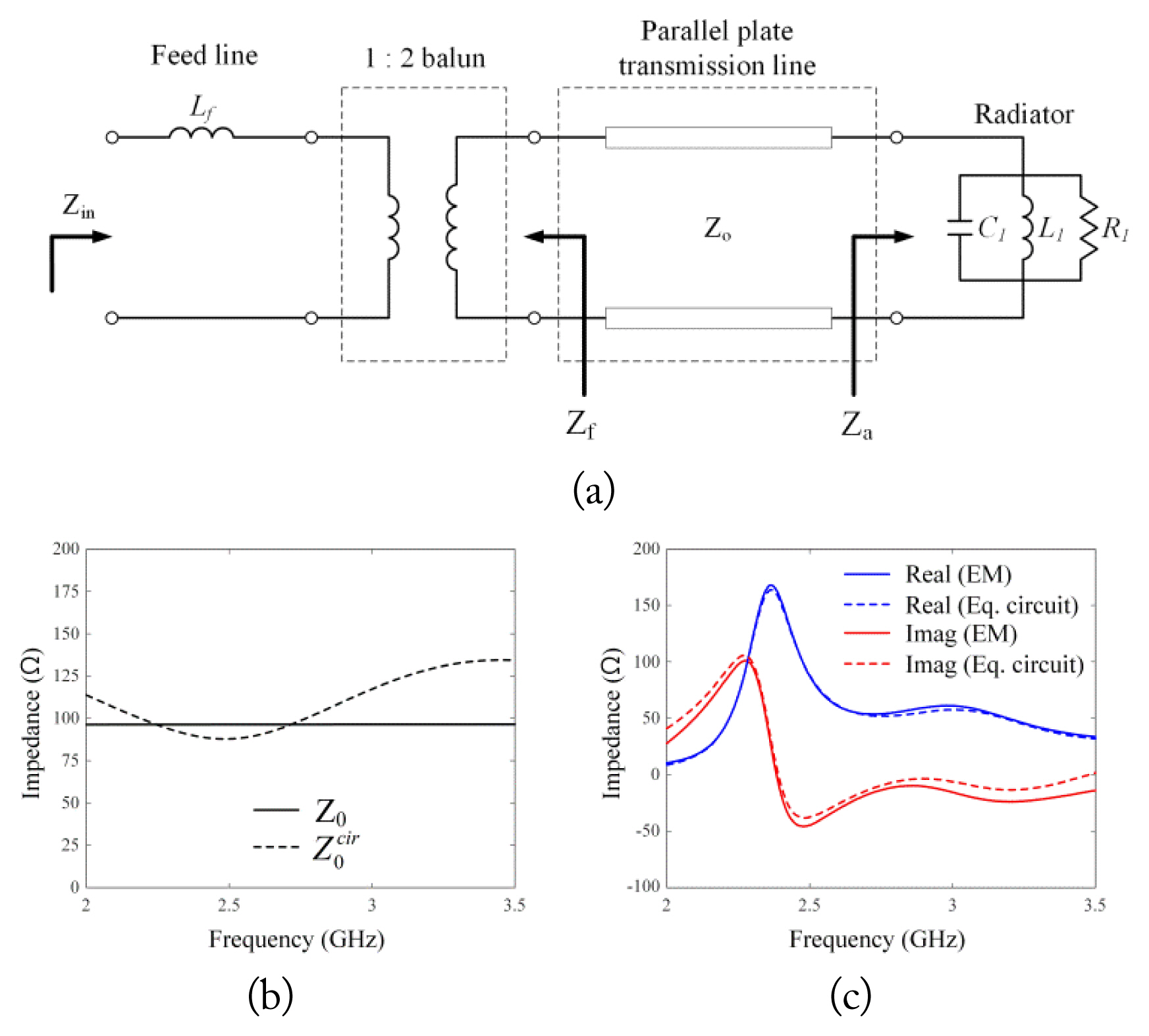
An equivalent circuit of the proposed antenna with a chip balun: (a) equivalent circuit model, (b) characteristic impedance responses of the parallel plate transmission line, (c) input impedance responses according to the frequency.
where
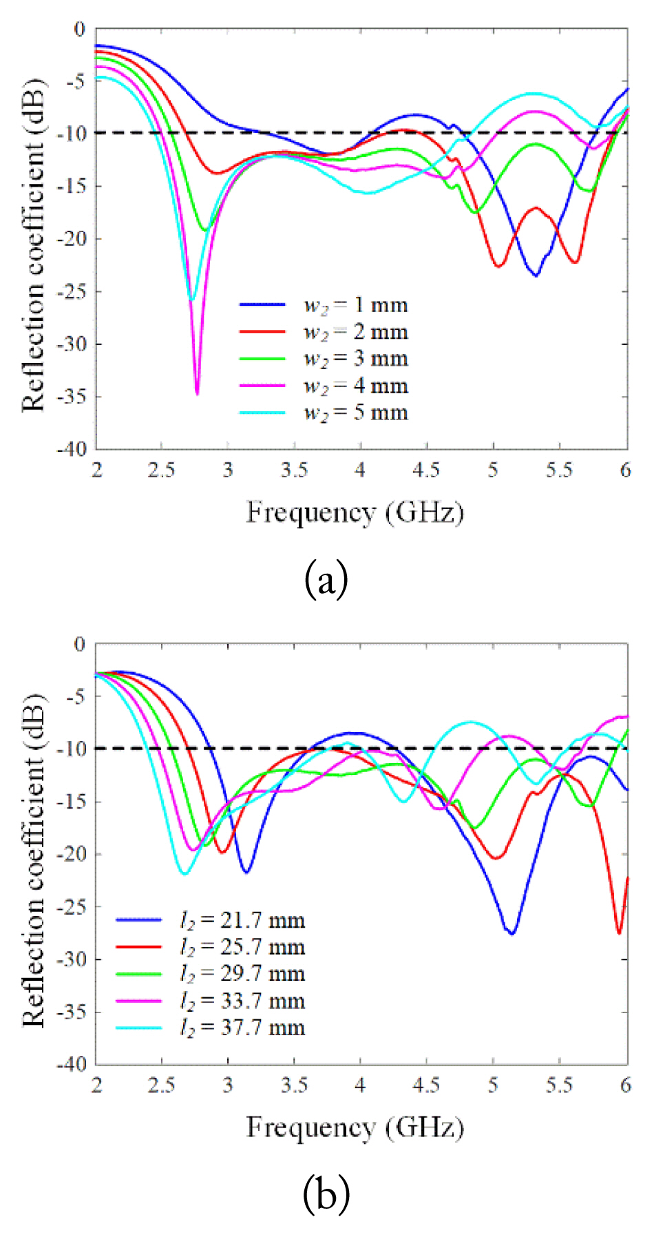
In addition, parametric studies of w2 and l2 are conducted to observe the sensitivity of the reflection coefficients, as shown in Fig. 8. Parameter w2 can adjust the reflection coefficient levels at the high-end frequency band, and l2 can affect the operating bandwidth due to the change in the capacitive couplings between the dipole radiator and ground. The optimum w2 of 3 mm and l2 of 29.7 mm are then obtained considering the stable reflection coefficient below −10 dB in the operating frequency band.
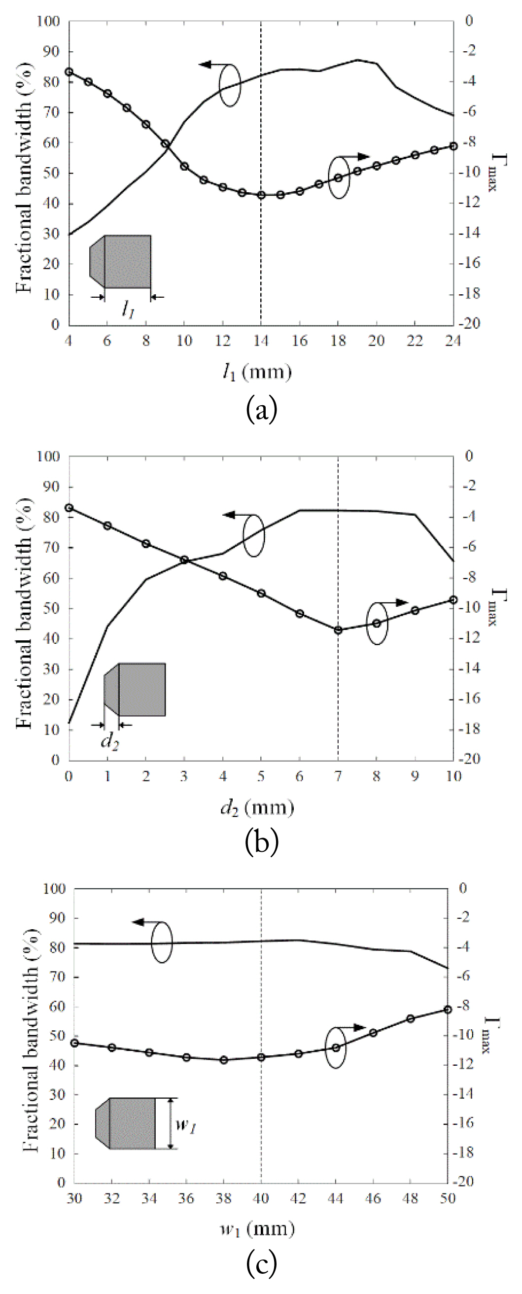
To further analyze the proposed antenna, parametric studies are conducted considering essential design parameters such as the radiator width (w1), length (l1), and truncated part (d2). In this analysis, we focus on the observation of the fractional bandwidth, and the maximum reflection coefficient. The maximum reflection coefficient is defined as Γmax to observe the stability of the wideband operation for the proposed antenna in the operating frequency band from 2.75 to 5 GHz. Fig. 9(a)–9(c) show the simulated parametric study results of the fractional bandwidth, and the maximum reflection coefficient. Results are obtained while varying the parameters in the ranges 4 mm ≤ l1 ≤ 24 mm, 0 mm ≤ d2 ≤ 10 mm, and 30 mm ≤ w1 ≤ 50 mm. Parametric studies indicate that the proposed antenna can achieve an over 80% fractional bandwidth with a Γmax of below −11.4 dB when using optimized parameters (dashed lines).
IV. Conclusion
In this paper, we proposed a wideband printed patch dipole antenna with a simple on-board feeding network. The proposed dipole antenna was printed on a substrate and was directly connected to the transmission line with the on-board balanced chip balun. The proposed antenna had measured and simulated fractional bandwidths of 79.5% and 83.4%, respectively. The simulated and measured gains were over 3 dBi in the frequency range of 2.75 to 4.5 GHz. The measured HPBWs were 107° and 86° in the zx- and zy-planes, respectively, at 3.5 GHz, and those at 4.5 GHz were 154° and 94°, respectively. To analyze the proposed antenna, an equivalent circuit was modeled, taking into account important antenna parts. The equivalent circuit results confirmed that the parallel transmission line of the proposed antenna worked as a quarter-wave transformer to achieve wideband characteristics. In addition, through parametric studies, the proposed antenna achieved over 80% stable fractional bandwidth with a Γmax of below −11.4 dB. For future work, additional or different designs will further be considered, such as a tapered transmission line and a cavity-backed ground to overcome the pattern distortion in the high-end frequency band.
Acknowledgments
This research has been supported by the Challenging Future Defense Technology Research and Development Program (No. 9127786) of Agency for Defense Development in 2019.
References
Biography

Jeongmin Cho received his B.S. degree in electronic and electrical engineering from Hongik University, Seoul, South Korea, in 2021. He is currently working toward his M.S. in electronic and electrical engineering from Hongik University, Seoul, South Korea. His research interests include shared aperture radar, wave propagation for radar applications, and X-band radar antennas.

Tae Heung Lim received his B.S., M.S., and Ph. D degrees in electronic and electrical engineering from Hongik University, Seoul, South Korea, in 2016, 2018, and 2022, respectively. He is currently working as a postdoctoral researcher in electrical engineering at Ulsan National Institute of Science and Technology (UNIST), South Korea. His research interests include global positioning system antennas, time-modulated arrays, antenna arrays, position optimization of array elements for adaptive beamforming, and wave propagations for radar applications.

Youngwan Kim received his B.S. and M.S. degrees in radio engineering from Kwangwoon University, Seoul, South Korea, in 2005 and 2007, respectively. He has been a chief research engineer with LIG Nex1, where he has been involved in the development of antennas for radar systems. His research interests include array antennas and metamaterials.

Hosung Choo received his B.S. degree in radio science and engineering from Hanyang University in Seoul, South Korea, in 1998, and his M.S. and Ph.D. degrees in electrical and computer engineering from the University of Texas at Austin, in 2000 and 2003, respectively. In September 2003, he joined the School of Electronic and Electrical Engineering, Hongik University, Seoul, South Korea, where he is currently a full-time professor. His principal areas of research are the use of optimization algorithms for developing antennas and microwave absorbers. His research includes the design of small antennas for wireless communications, reader and tag antennas for RFID, and on-glass and conformal antennas for vehicles and aircraft.
