J. Electromagn. Eng. Sci Search

CLOSE


J. Electromagn. Eng. Sci > Volume 23(2); 2023 > Article
Goudarzi, Lee, Kim, Park, and Han: Inverse Design of Terahertz Optical Power Splitters Using the Particle Swarm Optimization Method

Abstract

This letter proposes 50:50 TE terahertz power splitters based on digitized metamaterials. The components are optimized using the particle swarm optimization algorithm. The digitized metamaterials are formed as a silicon slab with circular air holes atop a silicon dioxide substrate. The insertion losses of optimized structures containing air holes with a radius of 9 μm and air holes with different radii (9 μm and 7 μm) are less than 3.9 dB and 3.65 dB, respectively, over a frequency range of 0.87–1.09 THz. The footprint of the proposed devices is 400 μm × 350 μm. The devices have excellent characteristics, such as compactness, efficiency, all-dielectric properties, and compatibility with CMOS fabrication technologies, and can become vital components of most terahertz-wave routing circuits.

I. Introduction

Terahertz technology has attracted considerable attention because terahertz waves can be exploited in wide-ranging applications, including medicine [13], security [4, 5], communications [68], and spectroscopy [911]. Diverse components for manipulating terahertz waves have been designed, including absorbers [1214], power splitters [1519], modulators [2022], polarization power splitters [2325], and sources [2630]. Among these components, terahertz power splitters (TPSs) are critically important in integrated circuits for dividing and routing terahertz waves to any point of the circuits. Homes et al. [17] proposed a TPS based on a silicon slab with a thickness of a few millimeters that can be used in spectroscopic measurements over a broad terahertz range (0.2–10 THz). Ung et al. [16] fabricated a TPS by depositing a thin silver sheet on an ultrathin, low-density polyethylene plastic sheet. By changing the thickness of the silver sheet and utilizing its skin depth, they varied the splitting ratios of the TPS, which they achieved through the transmission and reflection of the metallic dielectric structure in a frequency range of 0.5–1.5 THz. Hou et al. [19] proposed a TPS based on ferrite photonic crystals. They inserted line defects in the photonic crystals to steer the light and embedded two silicon and ferrite rods at the output branches to control the variable splitting ratio. In a magnetic field, the refractive index of the ferrite rod changed, and the splitting ratio could be varied. Reichel et al. [18] fabricated a TPS based on T-junction metallic structures. They created metallic waveguides to route the terahertz waves and a mechanical septum that changed the splitting ratio over a frequency range of 0.15–0.3 THz. Yang and Jiu-Sheng [15] realized a 1 × 6 TPS operating at 1 THz using temperature-dependent photonic crystals. By introducing line and point defects into the photonic crystals, they created a multimode interferometer and four Y splitters. However, these TPSs require an external magnetic field, which increases their fabrication cost [19], enlarges their dimensions [1519], and limits their integrability [1618].
Designing optical all-dielectric components is of great importance due to their low loss and high efficiency [3135]. In this letter, we present compact all-dielectric TPSs with an ultra-small footprint that are compatible with CMOS (complementary metal-oxide-semiconductor) fabrication technology. The TPSs were designed from metamaterials using an inverse design process based on particle swarm optimization (PSO), which optimizes the structures in a 50:50 splitting ratio. The finite-difference time-domain (FDTD) module of Lumerical software (Ansys, Vancouver, Canada) was used to simulate the structures.

II. Simulation Results and Discussion

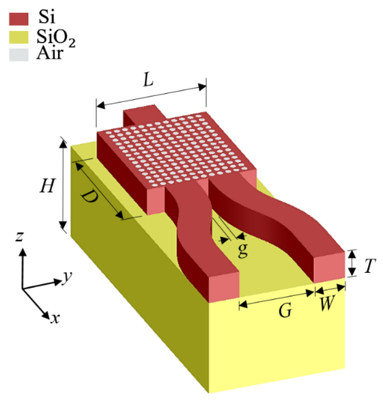
The devices have digitized structures made of a silicon slab with air holes deposited on a buried silicon dioxide substrate. They contain one input and two output waveguides, as shown in Fig. 1.
When designing a device using the PSO method, an initial structure is needed. The initial digitized structure consisted of a silicon (Si) slab etched with air holes deposited on a SiO2 substrate (Fig. 1). The radius of the air holes and the array period were 9 μm and 26 μm, respectively. The parameters L, D, H, G, g, W, and T (see Fig. 1 for their geometric descriptions) were set to 350, 400, 1,000, 237.6, 39.6, 100, and 100 μm, respectively. The region to be optimized was the region containing the circular holes, with dimensions of L × D × T. In this structure, the air holes were modeled as 1, and the silicon was modeled as 0. The insertion loss (IL), which is defined as −10log (Po/Pin) (where Po and Pin are the output power at the upper or lower branch and the incident power, respectively), was considered the figure of merit of the proposed device, which was minimized using the PSO method.
The structure was simulated using the three-dimensional (3D) FDTD method. The generation size and maximum generation number of the PSO method were 10 and 100, respectively. The mesh size of the 3D FDTD was dx = dy = dz = 3 μm. The waveguides were excited by a TE00 polarization mode with the electrical field component in the y-direction. The working frequency range of the device was 0.87–1.09 THz. Within this frequency range, the refractive indices of Si and SiO2 are 3.41 and 1.96, respectively.
Fig. 2 shows the structures after optimization using the PSO-based inverse design method. After optimization, a few circular air holes with optimized positions remained in the silicon slab on the SiO2 substrate. The inset of Fig. 2(a) displays the electromagnetic power distribution of the TE00 incident polarization mode at the cross-section of the input waveguide. The air holes in the optimized structure act as scatterer points. Aided by constructive interferences in the optimized region, the light is routed to the output branches. Moreover, these holes create a photonic bandgap that prevents the terahertz waves from diffracting in the y-direction; consequently, light can be guided only through the output branches. The sparsity of holes in the optimized region creates a guiding electromagnetic mode in the bandgap that steers the light to the outputs. Furthermore, using air holes with two different radii provides freedom for constructive interferences that result in higher transmission from the optimized digitized structure. Fig. 2(a) shows the optimized digitized structure containing air holes with a radius of 9 μm, and Fig. 2(b) shows the structure containing air holes with two different radii in the silicon slab.
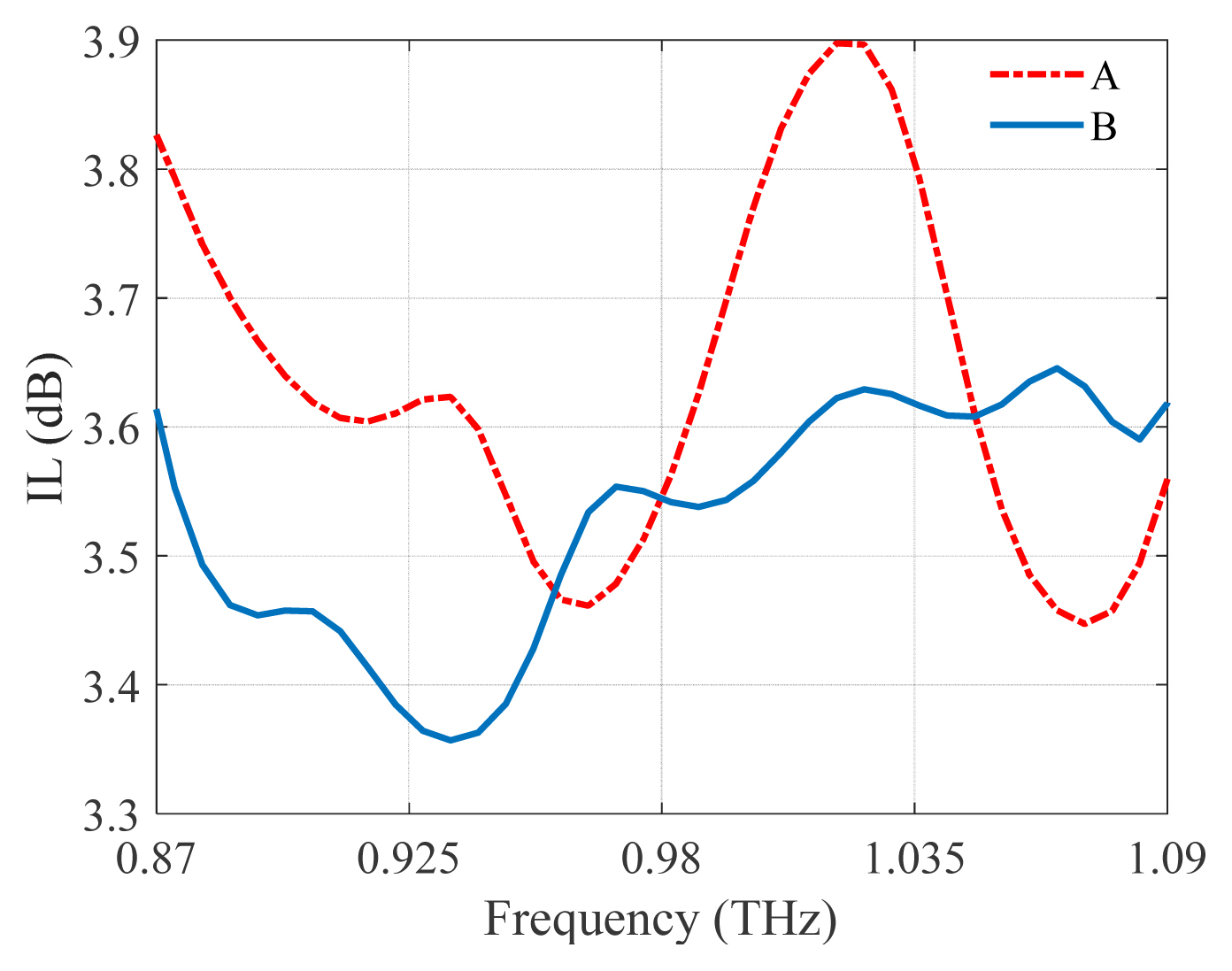
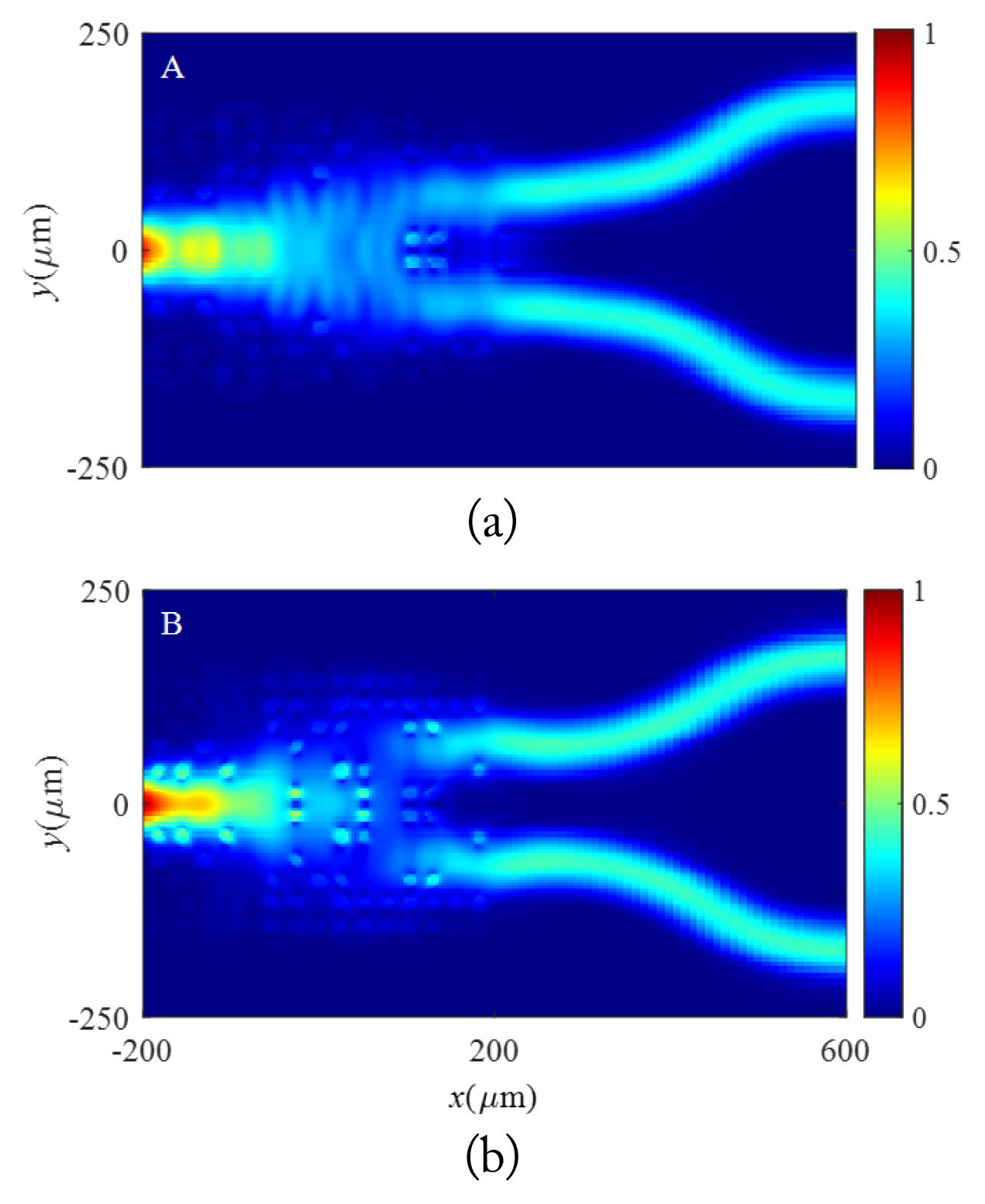
Fig. 3 shows the IL of the optimized 50:50 TPS structures containing air holes with one radius (structure A) and two different radii (structure B). The ILs of structures A and B were less than 3.9 dB and 3.65 dB, respectively, indicating efficiencies of approximately 81% and 86%, respectively, over a frequency range of 0.87–1.09 THz. Thus, structure B had higher efficiency than structure A. Moreover, the IL of structure B over this frequency range was flatter than that of structure A. The electromagnetic power distributions of the optimized structures A and B at a frequency of 0.94 THz are shown in Fig. 4(a) and 4(b), respectively. The distributions show the routes of the terahertz light in the optimized structures.
PSO is a bio-inspired stochastic algorithm for finding the optimal solution over the solution space. This optimization method has been used to design photonic devices [36, 37]. In this work, the PSO algorithm was used to minimize the IL. In this algorithm, N particles are considered, and Xi = (xi1, xi2, xi3, …, xid, …, xiD), Vi =(vi1, vi2, vi3, …, vid, …, viD), Pi =(pi1, pi2, pi3, …, pid, …, piD), and Pg =(pg1, pg2, pg3, …, pgd, …, pgD) are the position, velocity, optimal position, and swarm’s optimal position at each particle, respectively. D represents the dimension of the space that stands for the number of air holes inside the silicon slab. The velocity and position of particles at each iteration t are defined as
(1)
vi,t+1d=ωvi,td+c1r1(pi,td-xi,td)+c2r2(pg,td-xi,td),
(2)
xi,t+1d=xi,td+vi,t+1d,
where r1 and r2 are random numbers on the interval [0, 1], and c1, c2, and ω are social, cognitive, and inertial parameters, respectively. As shown in Fig. 5(a) and 5(b), the ILs converged roughly after 63 iterations, and the IL of structure B was less than that of structure A owing to the use of air holes with two different radii (7 μm and 9 μm). The IL parameter versus particles and iterations for the two structures is shown in Fig. 5(c) and 5(d). The IL decreased abruptly and then showed a further gradual decrease over iterations. The simulation time taken to design each structure using the PSO on a PC with a 2.9 GHz Core-i7 CPU and 32 GB of RAM was roughly 20 hours.
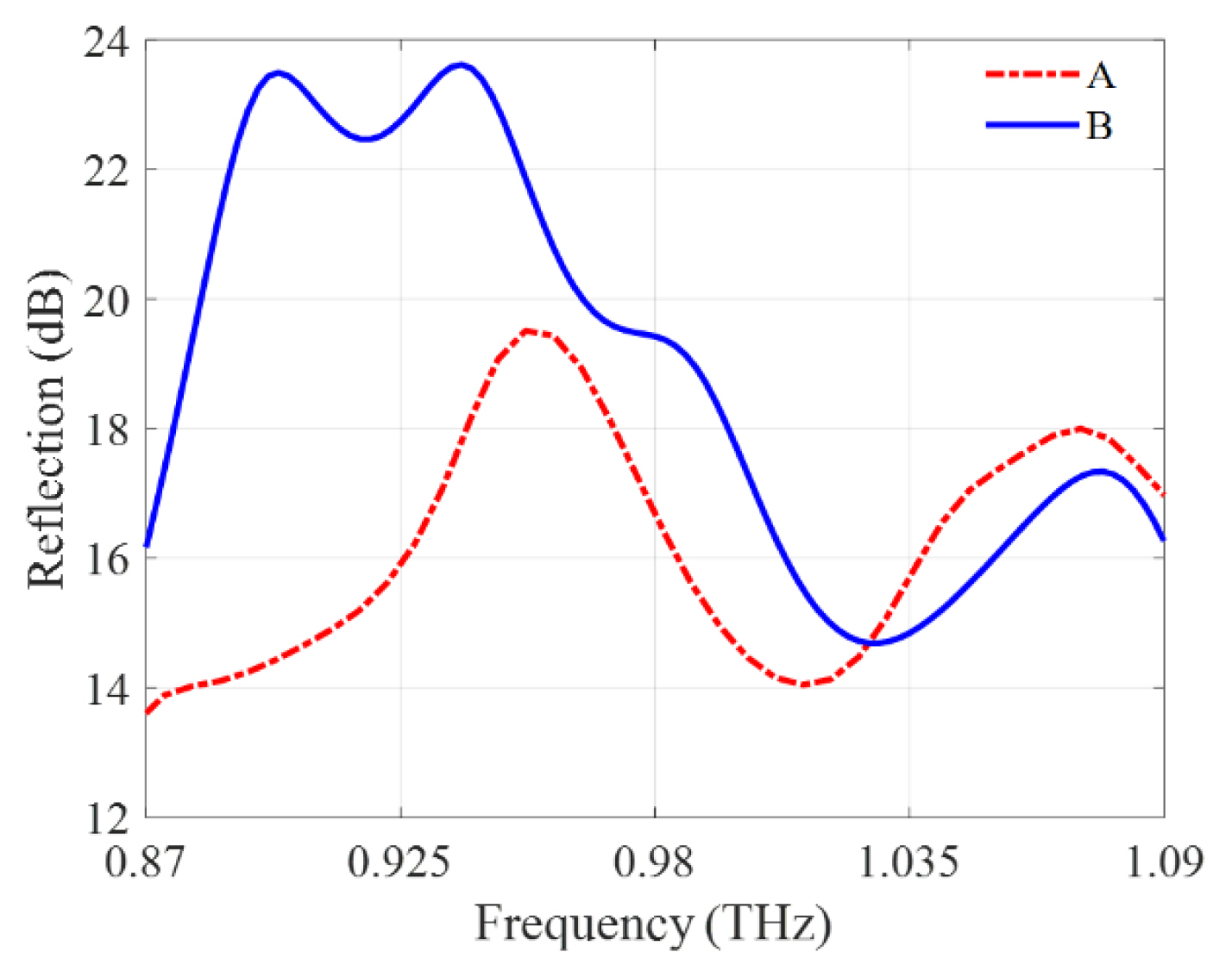
To show the return loss of structures A and B, the reflection at the input is defined as −10log(PRef/Pin), where PRef is the reflection at the input port. The reflection for the two structures is shown in Fig. 6. The reflection for structure A was higher than that of structure B over almost the entire working spectrum.

III. Conclusion

In this letter, we presented two 50:50 TE TPSs based on digitized metamaterials. The devices contain an input and two silicon waveguide outputs and were optimized using the PSO inverse design method. The structures consist of a silicon slab etched with a few air holes and deposited on a SiO2 substrate. The ILs of the optimized devices containing air holes with one radius and air holes with two different radii were less than 3.9 dB and 3.65 dB, respectively, over a frequency range of 0.87–1.09 THz. The advantages of the devices are compactness, efficiency, small footprint, all-dielectric properties, and compatibility with CMOS fabrication technology. These devices are suitable candidates for high-density terahertz circuits.

Acknowledgments

This work was supported by Samsung Electronics Co., Ltd. (IO201210-08035-01).

Fig. 1
Schematic of the initial structure of the terahertz power splitter.
jees-2023-2-r-153f1.jpg
Fig. 2
Schematic of the optimized terahertz power splitter (TPS) structures containing air holes with (a) a radius of 9 μm and (b) radii of 9 μm and 7 μm.
jees-2023-2-r-153f2.jpg
Fig. 3
Insertion loss (IL) versus frequency of an incident wave in TE00 mode for the optimized structures containing air holes with one radius (structure A) and two different radii (structure B).
jees-2023-2-r-153f3.jpg
Fig. 4
Distribution of electromagnetic power at a frequency of 0.94 THz in (a) structure A and (b) structure B.
jees-2023-2-r-153f4.jpg
Fig. 5
Insertion loss (IL) versus iterations for (a) structure A and (b) structure B. IL versus particles and iterations for (c) structure A and (d) structure B.
jees-2023-2-r-153f5.jpg
Fig. 6
Reflection at the input for structure A and structure B.
jees-2023-2-r-153f6.jpg

References

1. P.H. Siegel, "Terahertz technology in biology and medicine," IEEE Transactions on Microwave Theory and Techniques, vol. 52, no. 10, pp. 2438–2447, 2004.
crossref
2. M.A. Brun, F. Formanek, A. Yasuda, M. Sekine, N. Ando, and Y. Eishii, "Terahertz imaging applied to cancer diagnosis," Physics in Medicine & Biology, vol. 55, no. 16, article no. 4615, 2010. https://doi.org/10.1088/0031-9155/55/16/001
crossref pmid
3. S.W. Smye, J.M. Chamberlain, A.J. Fitzgerald, and E. Berry, "The interaction between terahertz radiation and biological tissue," Physics in Medicine & Biology, vol. 46, no. 9, article no. R101, 2001. https://doi.org/10.1088/0031-9155/46/9/201
crossref pmid
4. S. Ergun and S. Sonmez, "Terahertz technology for military applications," Journal of Management and Information Science, vol. 3, no. 1, pp. 13–16, 2015.
crossref
5. Y. Cheng, Y. Wang, Y. Niu, and Z. Zhao, "Concealed object enhancement using multi-polarization information for passive millimeter and terahertz wave security screening," Optics Express, vol. 28, no. 5, pp. 6350–6366, 2020.
crossref pmid
6. T. Harter, C. Fullner, J.N. Kemal, S. Ummethala, J.L. Steinmann, M. Brosi et al., "Generalized Kramers-Kronig receiver for coherent terahertz communications," Nature Photonics, vol. 14, no. 10, pp. 601–606, 2020.
crossref pdf
7. H. Sarieddeen, N. Saeed, T.Y. Al-Naffouri, and M.S. Alouini, "Next generation terahertz communications: a rendezvous of sensing, imaging, and localization," IEEE Communications Magazine, vol. 58, no. 5, pp. 69–75, 2020.
crossref
8. V. Petrov, D. Moltchanov, Y. Koucheryavy, and J.M. Jornet, "Capacity and outage of terahertz communications with user micro-mobility and beam misalignment," IEEE Transactions on Vehicular Technology, vol. 69, no. 6, pp. 6822–6827, 2020.
crossref pdf
9. P. Han, X. Wang, and Y. Zhang, "Time-resolved terahertz spectroscopy studies on 2D Van der Waals materials," Advanced Optical Materials, vol. 8, no. 3, article no. 1900533, 2020. https://doi.org/10.1002/adom.201900533
crossref pdf
10. J.A. Spies, J. Neu, U.T. Tayvah, M.D. Capobianco, B. Pattengale, S. Ostresh, and C.A. Schmuttenmaer, "Terahertz spectroscopy of emerging materials," The Journal of Physical Chemistry C, vol. 124, no. 41, pp. 22335–22346, 2020.
crossref
11. L.A. Sterczewski, J. Westberg, Y. Yang, D. Burghoff, J. Reno, Q. Hu, and G. Wysocki, "Terahertz spectroscopy of gas mixtures with dual quantum cascade laser frequency combs," ACS Photonics, vol. 7, no. 5, pp. 1082–1087, 2020.
crossref
12. O.M. Daraei, K. Goudarzi, and M. Bemani, "A tunable ultra-broadband terahertz absorber based on two layers of graphene ribbons," Optics & Laser Technology, vol. 122, article no. 105853, 2020. https://doi.org/10.1016/j.optlastec.2019.105853
crossref
13. H. Xiong, Q. Ji, T. Bashir, and F. Yang, "Dual-controlled broadband terahertz absorber based on graphene and Dirac semimetal," Optics Express, vol. 28, no. 9, pp. 13884–13894, 2020.
crossref pmid
14. K. Aidinis, O.M. Daraei, and K. Goudarzi, "Analytical design of tunable disk, patch and ribbon-patterned graphene absorbers in the terahertz spectrum," Photonics and Nanostructures-Fundamentals and Applications, vol. 46, article no. 100951, 2021. https://doi.org/10.1016/j.photonics.2021.100951
crossref
15. L. Yang and L. Jiu-Sheng, "Numerical analysis of temperature-controlled terahertz power splitter," Journal of the European Optical Society-Rapid Publications, vol. 13, article no. 12, 2017. https://doi.org/10.1186/s41476-017-0039-7
crossref pdf
16. B.S.Y. Ung, C. Fumeaux, H. Lin, B.M. Fischer, B.W.H. Ng, and D. Abbott, "Low-cost ultra-thin broadband terahertz beam-splitter," Optics Express, vol. 20, no. 5, pp. 4968–4978, 2012.
crossref pmid
17. C.C. Homes, G.L. Carr, R.P. Lobo, J.D. LaVeigne, and D.B. Tanner, "Silicon beam splitter for far-infrared and terahertz spectroscopy," Applied Optics, vol. 46, no. 32, pp. 7884–7888, 2007.
crossref pmid
18. K.S. Reichel, R. Mendis, and D.M. Mittleman, "A broadband terahertz waveguide T-junction variable power splitter," Scientific Reports, vol. 6, no. 1, article no. 28925, 2016. https://doi.org/10.1038/srep28925
crossref pmid pmc pdf
19. Y. Hou, F. Fan, X.H. Wang, and S.J. Chang, "Terahertz power splitter based on ferrite photonic crystal," Optik, vol. 124, no. 22, pp. 5285–5288, 2013.
crossref
20. A. Jakhar, P. Kumar, A. Moudgil, V. Dhyani, and S. Das, "Optically pumped broadband terahertz modulator based on nanostructured PtSe2 thin films," Advanced Optical Materials, vol. 8, no. 7, article no. 1901714, 2020. https://doi.org/10.1002/adom.201901714
crossref pdf
21. H.T. Chen, W.J. Padilla, M.J. Cich, A.K. Azad, R.D. Averitt, and A.J. Taylor, "A metamaterial solid-state terahertz phase modulator," Nature Photonics, vol. 3, no. 3, pp. 148–151, 2009.
crossref pdf
22. A. Jakhar, P. Kumar, S. Husain, V. Dhyani, and S. Das, "Integration of nanometer-thick 1T-TaS2 films with silicon for an optically driven wide-band terahertz modulator," ACS Applied Nano Materials, vol. 3, no. 11, pp. 10767–10777, 2020.
crossref
23. H. Zeng, Y. Zhang, F. Lan, S. Liang, L. Wang, T. Song et al., "Terahertz dual-polarization beam splitter via an anisotropic matrix metasurface," IEEE Transactions on Terahertz Science and Technology, vol. 9, no. 5, pp. 491–497, 2019.
crossref
24. W.S. Lee, S. Nirantar, D. Headland, M. Bhaskaran, S. Sriram, C. Fumeaux, and W. Withayachumnankul, "Broadband terahertz circular-polarization beam splitter," Advanced Optical Materials, vol. 6, no. 3, article no. 1700852, 2018. https://doi.org/10.1002/adom.201700852
crossref pdf
25. C.W. Berry and M. Jarrahi, "Broadband terahertz polarizing beam splitter on a polymer substrate," Journal of Infrared, Millimeter, and Terahertz Waves, vol. 33, pp. 127–130, 2012.
crossref pdf
26. A.H. Esmaeili, S. Matloub, A. Rostami, and K. Goudarzi, "Microwave source with enhanced radiation power based on orbitron MASERs," Journal of Instrumentation, vol. 15, article no. P01016, 2020. https://doi.org/10.1088/1748-0221/15/01/P01016
crossref pmid pmc pdf
27. A.H. Esmaeili and K. Goudarzi, "Half-cylindrical grating structure for enhancing radiation power of Smith–Purcell emitter," Optical Engineering, vol. 58, no. 10, article no. 103107, 2019. https://doi.org/10.1117/1.OE.58.10.103107
crossref
28. K. Goudarzi, S. Matloub, and A. Rostami, "Aperiodic graphene ribbons in MOSFET topology for multiwavelength terahertz generation," Optical and Quantum Electronics, vol. 51, article no. 254, 2019. https://doi.org/10.1007/s11082-019-1971-0
crossref pdf
29. K. Goudarzi, S. Matloub, and A. Rostami, "Generation of two-color terahertz radiation using Smith–Purcell emitter and periodic dielectric layers," Optical and Quantum Electronics, vol. 51, article no. 48, 2019. https://doi.org/10.1007/s11082-019-1749-4
crossref pdf
30. K. Goudarzi, S. Matloub, and A. Rostami, "Multiwavelengths terahertz emitter using graphene aperiodic super-cells," Optik, vol. 179, pp. 379–384, 2019.
crossref
31. K. Goudarzi, A. Mir, I. Chaharmahali, and D. Goudarzi, "All-optical XOR and OR logic gates based on line and point defects in 2-D photonic crystal," Optics & Laser Technology, vol. 78, no. Part B, pp. 139–142, 2016.
crossref
32. K. Goudarzi and M. Lee, "Super strong wide TM Mie bandgaps tolerating disorders," Scientific Reports, vol. 12, article no. 7884, 2022. https://doi.org/10.1038/s41598-022-11610-0
crossref pmid pmc pdf
33. K. Goudarzi, H.G. Maragheh, and M. Lee, "Calculation of the Berry curvature and Chern number of topological photonic crystals," Journal of the Korean Physical Society, vol. 81, no. 5, pp. 386–390, 2022.
crossref pdf
34. K. Goudarzi, "Ultra-narrow, highly efficient power splitters and waveguides that exploit the TE01 Mie-resonant bandgap," Optics Express, vol. 29, no. 21, pp. 32951–32965, 2021.
crossref pmid
35. K. Goodarzi and A. Mir, "Design and analysis of an alloptical Demultiplexer based on photonic crystals," Infrared Physics & Technology, vol. 68, pp. 193–196, 2015.
crossref
36. K. Goudarzi and M. Lee, "Inverse design of a binary waveguide crossing by the particle swarm optimization algorithm," Results in Physics, vol. 34, article no. 105268, 2022. https://doi.org/10.1016/j.rinp.2022.105268
crossref
37. Z. Ma and Y. Li, "Parameter extraction and inverse design of semiconductor lasers based on the deep learning and particle swarm optimization method," Optics Express, vol. 28, no. 15, pp. 21971–21981, 2020.
crossref pmid

Biography

jees-2023-2-r-153i1.jpg
Kiyanoush Goudarzi received a Ph.D. degree in electrical engineering from the University of Tabriz in 2019. From 2020 to the present, he has been a postdoctoral researcher at POSTECH. His current research interests include topological photonics and photonic integrated circuits.

Biography

jees-2023-2-r-153i2.jpg
Han-eol Lee received a B.S. degree in physics from Chonnam National University, Gwangju, Republic of Korea, in 2018. He received an M.S. in electronic engineering from the Pohang University of Science and Technology, Pohang, Republic of Korea, in 2022. He is currently pursuing a Ph.D. in electronic engineering at the Pohang University of Science and Technology. His current research interests include terahertz photonics and metamaterial design.

Biography

jees-2023-2-r-153i3.jpg
Doyoung Kim received a B.S. degree in electronic and electrical engineering from Dongguk University, Seoul, South Korea, in 2017. He received an M.S. in electronic engineering from the Pohang University of Science and Technology, Pohang, Republic of Korea, in 2022. His current research interests include terahertz photonics and metamaterial design.

Biography

jees-2023-2-r-153i4.jpg
Ikmo Park was a B.S. degree in electrical engineering from the State University of New York at Stony Brook and M.S. and Ph.D. degrees in electrical engineering from the University of Illinois at Urbana-Champaign. He joined the Department of Electrical and Computer Engineering of Ajou University in 1996. Prior to joining Ajou University, he worked in the Device & Materials Laboratory of the LG Corporate Institute of Technology, Seoul, Republic of Korea, where he engaged in the research and development of various antennas for personal communication systems, wireless local area networks, and direct broadcasting systems. He was a visiting professor at the Department of Electrical and Computer Engineering of POSTECH, Pohang, Republic of Korea, from March 2004 to February 2005 and the Department of Electrical and Computer Engineering of the University of Arizona, Tucson, Arizona, USA, from July 2011 to June 2012. He has authored and coauthored over 300 technical journal and conference papers. He also holds over 50 domestic and international patents. He served as chair of the Department of Electrical and Computer Engineering of Ajou University. He is a member of the board of directors of the Korea Institute of Electromagnetic Engineering and Science (KIEES). He serves as the editor-in-chief of the KIEES Proceedings and the Journal of KIEES, as an editorial board member for the International Journal of Antennas and Propagation, and as an associate editor for IET Electronics Letters. He served as an editorial board member of the Journal of Electromagnetic Engineering and Science. He is also a member of Eta Kappa Nu and Tau Betta Pi.

Biography

jees-2023-2-r-153i5.jpg
Haewook Han received B.S. and M.S. degrees in electrical engineering from Seoul National University, Seoul, Republic of Korea, in 1986 and 1988, respectively. He received a Ph.D. degree in electrical engineering from the University of Illinois at Urbana-Champaign, USA, in 1995. From 1995 to 1997, he conducted semiconductor laser research at AT&T Bell Laboratories, Murray Hill, USA. He is currently a professor of electronic engineering at the Pohang University of Science and Technology, Pohang, Republic of Korea. His current research interests include nano-bio terahertz photonics, compact terahertz sources (antennas and photomixers), high-precision and real-time terahertz comb spectroscopy, terahertz photonic crystal fibers, terahertz biomedical sensing and imaging, terahertz near-field microscopy, terahertz hydration dynamics in biomolecular systems, and nanophotonic CMOS image sensors.
TOOLS
Share :
Facebook Twitter Linked In Google+
METRICS Graph View
  • 1 Crossref
  • 0 Scopus
  • 1,126 View
  • 63 Download
Related articles in JEES

ABOUT
ARTICLE CATEGORY

Browse all articles >

BROWSE ARTICLES
AUTHOR INFORMATION
Editorial Office
#706 Totoo Valley, 217 Saechang-ro, Yongsan-gu, Seoul 04376, Korea
Tel: +82-2-337-9666    Fax: +82-2-6390-7550    E-mail: admin-jees@kiees.or.kr                

Copyright © 2024 by The Korean Institute of Electromagnetic Engineering and Science.

Developed in M2PI

Close layer
prev next