I. Introduction
In wireless systems, a balun is vital in converting unbalanced signals to balanced ones or vice versa. Traditionally, baluns are made in low-temperature co-fired ceramic (LTCC) and monolithic microwave integrated circuits (MMIC) technologies. Commercially, baluns are implemented in LTCC technology, but recently, there has been a movement of technology to integrated passive device (IPD) technology for miniaturization and integrated circuits. Much research has been conducted to incorporate individual baluns [
1,
2]. Most of them are baluns using transmission lines developed for RF applications. The circuits using transmission line topology are larger in size because of multiple λ/4 wavelengths.
Thus, many papers have suggested that the lumped LC passive component provide a size reduction [
3–
9]. However, these papers’ suggestion has the effect of reducing the target bandwidth due to frequency-dependent factors. The conventional work in [
10] is implemented with low-pass filter (LPF) and high-pass filter (HPF) structures using lumped elements, but it is difficult to obtain a uniform magnitude characteristic. Thus, magnitude balance and phase difference are uniform only at the center frequency. However, as magnitude balance deviates from the center frequency, the magnitude and phase deviation increase.
In this paper, we propose a wideband balun using through-silicon via (TSV) IPD technology. The TSV process provides a solid ground plane with a copper layer at the wafer’s backside. The design minimizes GND influence from external packaging variation sources, and the overall tolerance is primarily controlled by the wafer manufacturing variation [
11]. Reduced thermal resistance through the backside via [
12] and excellent thermal conductivity of evenly distributed thick copper plane improves thermal performance, which is critical for compatible use with high-power gallium nitride (GaN). The proposed balun is composed of lumped components, and the component values are derived by differentiating the magnitude of the
S-parameter with the constant value. The proposed balun implemented using IPD technology to smaller and low loss.
II. Design Theory and Simulation Results
1. Design Theory
An ideal balun consists of distributed lines using λ/4 and 3λ/4 of differential electrical lengths with
2Z0to maintain a phase difference of 180°.
Fig. 1(a) shows a balun consisting of lumped elements L
1, L
2, C
1, C
2, and C
3, which are from the distributed balun.
Fig. 1(b) shows the proposed balun modified from
Fig. 1(a). The left sides between Ports 1 and 2 are from the equivalent circuit of the low pass type, while the right sides between Ports 1 and 3 are from the circuit of the high pass type. The conventional circuit of
Fig. 1(a) has a magnitude balance problem. To improve the magnitude balance, we add L
P and C
P parallel resonators at the center point of L
1 in the circuit where the C
2 and L
2 have been removed, as shown in
Fig. 1(b). The half-point of the L
1 is where the values of L
2P and L
1P are the same. Similarly, we insert a parallel resonator at the doubling point of C
1, where 2C
1 = C
1P = C
2P.
The inserted parallel resonator is an open circuit at the resonant frequency, and the inserted resonator serves to control the deviated magnitude values to constant values. To derive the element values of the proposed circuit of
Fig. 1(b),
Eq. (1) is obtained by terminating Port 3 as
Z0, which is the ABCD parameter between Ports 1 and 2.
Similarly, the ABCD parameters obtained between Ports 1 and 3 are derived by A
2, B
2, C
2, and D
2, as shown in
Eq. (2). The input admittance Y
in terminated as Y
0 at Port 3 in
Fig. 1(b) is expressed as
Eq. (3).
The total ABCD parameter is obtained between Ports 1 and 2 using the cascaded Y
in and A
1, B
1, C
1, and D
1 parameters as
Eq. (4).
Eq. (4) is arranged as A
T = A
1, B
T = B
1, C
T = A
1Y
in + C
1, and D
T = B
1Y
in + D
1. Using the relation between the
S-parameter and the ABCD parameter,
S21 is obtained as
Eq. (5).
The magnitude of
S21 is shown as
Eq. (6).
By differentiating the magnitude of the derived |
S21|, the derived |
S21| must be frequency independent in terms of the frequency over a wide bandwidth. The differential value of the derived |
S21| at the center frequency
ω0 is zero to make the frequency-dependent term reduced in wideband; then the value of L
P is expressed as
Eq. (7).
The CP of the inserted parallel resonant values are derived from the resonant circuit.
2. Circuit Simulation Results
To verify the derived theory, the conventional circuit in
Fig. 1(a) and the proposed circuit in
Fig. 1(b) must be compared. The center frequency is 3.6 GHz, and the conducted simulation tool is Ansys, Electronics Desktop. The obtained values of
Fig. 1(a) and 1(b) are shown in
Table 1.
Fig. 2(a) and 2(b) show the circuit simulation results of the conventional and proposed circuits. The conventional circuit has variations ranging from −2.3 to −5.8 dB, while the proposed circuit has a constant value from −2.893 to −3.117 dB from 2.8 to 4.4 GHz. From the simulation results, the magnitude balance of the proposed circuit is compensated using design theory.
III. 3D Structure and Fabrication Results
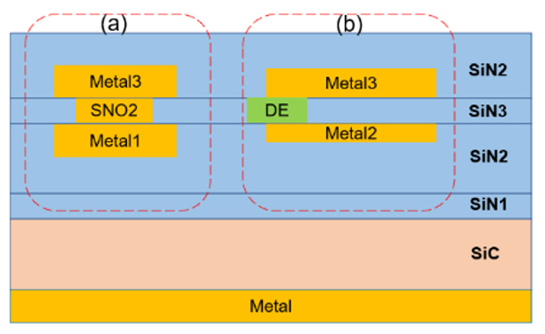
Fig. 3(a) and 3(b) show the layer configuration of the IPD inductor and capacitor, respectively. It is a cross-section view in which several layers of silicon nitride (SiN) and metal are stacked on silicon carbide (SiC). The inductor consists of M
1 (Metal1) and M
3 (Metal3) layers and is implemented in the form of a spiral inductor using M
1 of the SiN
2 layer. Then, the M
1 and M
3 layers are connected using the SNO
2 (SiN open) metal layer penetrating the SiN
3 dielectric (DE) layer. The capacitor uses M
2 and M
3 layers and is implemented in the form of a metal-insulator-metal (MIM) capacitor by inserting a SIN
3 DE layer between the metals. A DE layer is inserted between each metal layer of the inductor and capacitor to prevent short circuits.
Table 2 shows the details of the layers used in the structure of
Fig. 3.
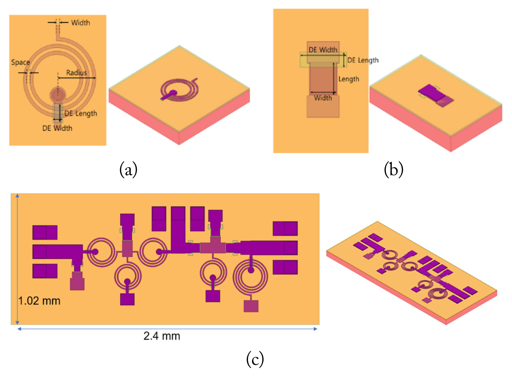
Fig. 4(a) and 4(b) show a spiral inductor and capacitor implemented as an IPD, respectively. Inductors require 1.56 nH and 3.12 nH for the design of the proposed balun at 3.6 GHz. Capacitors require 1.2 pF and 0.56 pF for the proposed balun.
Fig. 4(c) is the proposed balun. The ground passing through the SiC layer is designed using the TSV method, which is implemented in the circuit in the form of back via (BVIA). In addition, the designed ground-signal-ground (GSG) pad is inserted at the input and output ports for measurement. The total size of
Fig. 4(c) is 2.4 mm × 1.02 mm.
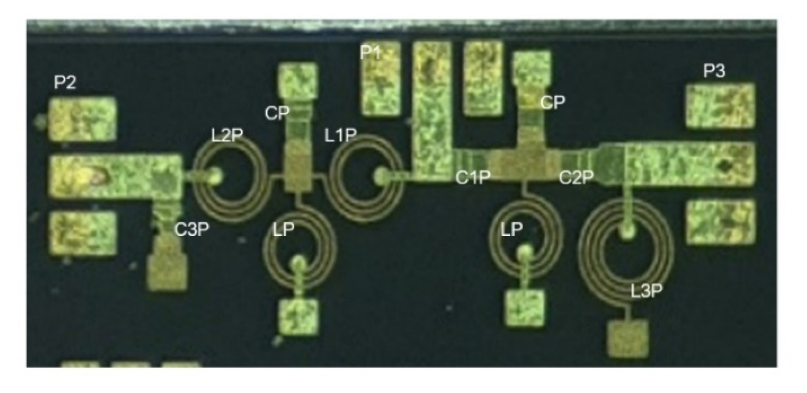
Fig. 5 is the microphotograph of the proposed balun fabricated by an IPD. The implemented structure shows that the designed 3D structure is well implemented.
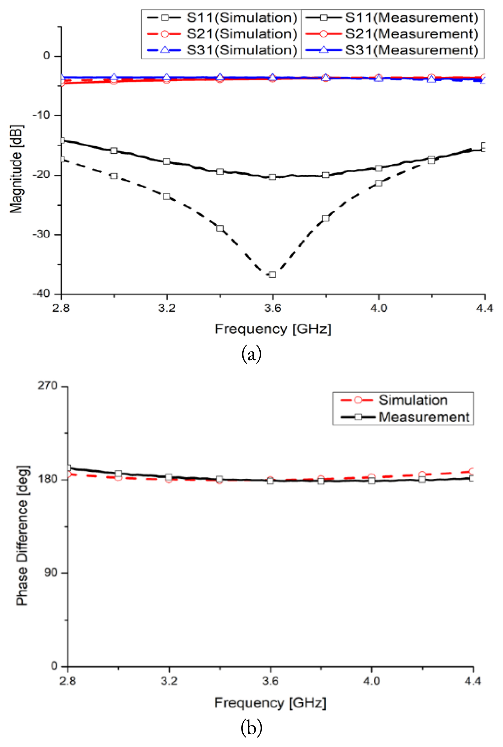
Fig. 6(a) and 6(b) show the magnitude and phase difference results measured with Agilent Network Analyzer (N5230) by uploading the proposed balun made with an IPD to Cascade Microtech probe station (Probe station summit 11741B).
Fig. 6(a) is the comparison results according to the ±0.2 dB magnitude results within 2.96–4.2 GHz.
Fig. 6(b) is the comparison results according to the phase difference from 2.96–4.2 GHz with ±3°. The measured results have a fabrication error since the capacitor is dominantly affected by the DE thickness between metals.
The comparison results of the performance according to the IPD technology are listed in
Table 3, which shows that the balun has the center frequency, amplitude imbalance, phase imbalance, and fractional bandwidth (FBW) based on a 15-dB return loss. Therefore, using the proposed design method, the proposed circuit has excellent measurement results according to the amplitude, phase imbalance, and FBW.
IV. Conclusion
In this paper, we proposed a wideband balun using IPD technology for smaller sizes and low insertion loss. The proposed balun is designed to maintain the magnitude slope constant. By differentiating the magnitude, the component values of the proposed balun are derived. The magnitude balance and phase differences resulted in about 0.2 dB and 3° from 2.96 to 4.2 GHz. Thus, the frequency dependency of the proposed circuit is well compensated for not only magnitude balance but also phase difference.
Acknowledgments
This result was supported by “Regional Innovation Strategy (RIS)” through the National Research Foundation of Korea (NRF) funded by the Ministry of Education (MOE) (No. 2021RIS-004) and the Soonchunhyang University Research Fund.
Fig. 1
(a) Balun using lumped components from the distributed line and (b) proposed balun using
Fig. 1(a).
Fig. 2
Comparison results of conventional and proposed baluns: (a) the magnitude and (b) the enlarged magnitude of S21 and S31.
Fig. 3
Layer structure of the IPD: (a) inductor and (b) capacitor.
Fig. 4
(a) The IPD structure of the inductor, (b) the IPD structure of the capacitor, and (c) the 3D structure of the proposed IPD balun.
Fig. 5
Microphotograph of the fabricated balun.
Fig. 6
Comparison results between the 3D structure and measured results of
Fig. 4: (a) magnitude results and (b) phase difference results.
Table 1
Element values of the conventional and proposed circuits
Circuit |
Value |
Conventional balun (L[nH], C[pF]) |
L1
|
3.12 |
L2
|
3.12 |
L3
|
3.12 |
C1
|
0.62 |
C2
|
0.62 |
C3
|
0.62 |
Proposed balun (L[nH], C[pF]) |
L1P
|
1.56 |
L2P
|
1.56 |
L3P
|
3.12 |
C1P
|
1.25 |
C2P
|
1.25 |
C3P
|
0.62 |
LP
|
1.56 |
CP
|
1.25 |
Table 2
Layer |
Relative permeability |
Dielectric loss tangent |
Conductivity (S/m) |
Thickness (μm) |
SiC |
9.7 |
0.027 |
- |
85 |
SiN1 |
8.5 |
0.0036 |
- |
0.12 |
SiN2 |
8.5 |
0.0036 |
- |
5.25 |
SiN3 |
7.9 |
0.0036 |
- |
0.25 |
SiN4 |
8.5 |
0.0036 |
- |
4.75 |
DE |
3.7 |
0.028 |
- |
0.25 |
Metal1 |
- |
- |
4.1e7
|
5 |
Metal2 |
- |
- |
3.8e7
|
1.5 |
Metal3 |
- |
- |
4.1e7
|
4.5 |
Metal |
- |
- |
4.1e7
|
8 |
Table 3
Performance comparison results of the previous works
Study |
f0 (MHz) |
Fabrication |
Number of elements |
Amplitude imbalance (dB) |
Phase imbalance (°) |
FBWa (%) |
Yang et al. [8] |
4,035 |
IPD |
8 |
0.35 |
5.26 |
16.7 |
Li et al. [9] |
2,400 |
IPD |
6 |
0.5 |
0.5 |
8 |
Kumar et al. [10] |
2,400 |
IPD |
7 |
0.47 |
3 |
- |
This work |
3,600 |
IPD |
10 |
0.2 |
3 |
34.4 |
References
1. A.Q. Liu, A.B. Yu and Q.X. Zhang, "Broad-band band-pass and band-stop filters with sharp cut-off frequencies based on series CPW stubs," In:
Proceedings of 2006 IEEE MTT-S International Microwave Symposium Digest; San Francisco, CA. 2006; pp 353–356.
2. W. Na, J. Song, I.H. Cho, K.K. Ryu and M.Q. Lee, "Ring hybrid balun with good amplitude and phase balance," In:
Proceedings of 2007 IEEE/MTT-S International Microwave Symposium; Honolulu, HI. 2007; pp 1769–1772.
3. K.S. Ang, Y.C. Leong and C.H. Lee, "Analysis and design of miniaturized lumped-distributed impedance-transforming baluns,"
IEEE Transactions on Microwave Theory and Techniques, vol. 51, no. 3, pp. 1009–1017, 2003.
4. C.W. Tang and C.Y. Chang, "LTCC-MLC chip-type balun realised by LC resonance method,"
Electronics Letters, vol. 38, no. 11, pp. 519–520, 2002.
5. C.W. Tang and C.Y. Chang, "A semi-lumped balun fabricated by low temperature co-fired ceramic," In: Proceedings of 2002 IEEE MTT-S International Microwave Symposium Digest (Cat. No. 02CH37278); Seattle, WA. 2002; pp 2201–2204.
6. J.C. Park, J.Y. Park and H.S. Lee, "Fully embedded 2.4 GHz LC-balun into organic package substrate with series resonant tank circuit," In:
Proceedings of 2007 IEEE/MTT-S International Microwave Symposium; Honolulu, HI. 2007; pp 1901–1904.
7. Z.Y. Zhang, Y.X. Guo, L.C. Ong and M.Y.W. Chia, "A new wide-band planar balun on a single-layer PCB,"
IEEE Microwave and Wireless Components Letters, vol. 15, no. 6, pp. 416–418, 2005.
8. Y. Yang, Y. Wu, Z. Zhuang, M. Kong, W. Wang and C. Wang, "An ultraminiaturized bandpass filtering Marchand balun chip with spiral coupled lines based on GaAs integrated passive device technology,"
IEEE Transactions on Plasma Science, vol. 48, no. 9, pp. 3067–3075, 2020.
9. Y. Li, C. Wang and N.Y. Kim, "A high performance compact Wilkinson power divider using GaAs-based optimized integrated passive device fabrication process for LTE application,"
Solid-State Electronics, vol. 103, pp. 147–153, 2015.
10. A. Kumar, F.Y. Meng, C. Wang, K.K. Adhikari, T. Qiang, Q. Wu and Y. Wu, "Design analysis of integrated passive device-based balun devices with high selectivity for mobile application,"
IEEE Access, vol. 7, pp. 23169–23176, 2019.
11. K.R. Shin, J. Arendell and K. Eilert, "Compact 5G n77 band pass filter with through silicon via (TSV) IPD technology," In:
Proceedings of 2019 IEEE 20th Wireless and Microwave Technology Conference (WAMICON); Cocoa Beach, FL. 2019; pp 1–3.
12. J.S. Kofol, B.J.F. Lin, M. Mierzwinski, A. Kim, A. Armstrong and R. Van Tuyl, "A backside via process for thermal resistance improvement demonstrated using GaAs HBTs," In:
Proceedings of the GaAs IC Symposium Technical Digest; Miami Beach, FL. 1992; pp 267–270.
Biography
Youna Jang received her master’s in display engineering from Hanyang University, Seoul, Korea, in 2014. She also received her Ph.D. in electrical communication system engineering from Soonchunhyang University, Choongnam, Korea, in 2019. She participated as a designer of the Duplexer filter in an internship program in 2015 at Qorvo, Bundang, South Korea. She was a lecturer at Soonchunhyang University from 2016 to 2020. She is currently a research professor at the Radio and Mechatronics Research Center. Her research areas include the design of passive components in microwave bands.
Biography
Kwanhun Jeong was born in Mokpo, Korea, in 1994. He received his B.E. degree in electrical engineering from Soonchunhyang University, Asan, Korea, in 2020. Currently, he received his master’s in ICT convergence at Soonchunhyang University. His current research interests include RF passive device theory, design, and testing. Currently, he joins the FAB Group at Wavice.
Biography
Yea-Ji Lee was born in Seoul, South Korea, in 1996. She received her bachelor’s in electrical engineering from Soonchunhyang University, Asan, South Korea. She received his master’s in ICT convergence at Soonchunhyang University. Her current research interests include RF filter design and testing and passive device. Currently, she joins the Interconnect Part team at Gigalane.
Biography
Taehoon Kang was born in Incheon, Korea, in 1993. He received his M.S. degree from Soonchunhyang University, Asan, Korea, in 2019. Currently, he is studying for a Ph.D. at Soonchunhyang University. His current research interests include RF filter theory, design, and testing.
Biography
Sangmin Lee received his Ph.D. in solid state Physics at Sogang University, Korea, in 1996. From 1996 to 1998, he was a postdoc at ETRI, developing InP-based photonic integrated circuits. From 2000 to 2005, he worked at UCSB and GCS, developing InP-based DHBT devices. In 2005, he started working on GaN HEMT devices for RF applications at various companies in the US, including RFMD and Cree. He was a qualification manager at RFMD and a research scientist at Cree. He joined the GaN HEMT R&D team at Gigalane in 2015, which became Wavice in 2017, as a CTO working on the R&D of RF GaN HEMT device technologies. He is currently a vice president of technonlogy at Global Communication Semiconductors, LLC in California, USA.
Biography
Seo Koo was born in Seoul, Korea, in 1990. He received his M.S. degree from Soonchunhyang University, Asan, Korea, in 2018. Currently, he is studying for a Ph.D. at Soonchunhyang University. His current research interests include RF filter theory, design, and testing.
Biography
Dal Ahn received his B.S., M.S., and Ph.D. degrees in electronics from Sogang University, Seoul, Korea, in 1984, 1986, and 1990, respectively. From 1990 to 1992, he worked with the Mobile Communications Division, Electronics, and Telecommunications Research Institute (ETRI), Daejeon, Korea. Since 1992, he has been affiliated with the department of Electrical Engineering, Soonchunhyang University, Asan, Chungnam, Korea, where he is currently a professor. Currently, he is also the chief of the RF and Microwave Component Research Center (RAMREC) at Soonchunhyang University. In addition, he is a technical consultant for Tel Wave Inc., Suwon, Korea. His current research interests include the design and application of passive and active components at radio and microwave frequencies, the design of RF front-end modules for various handset systems using low-temperature co-fired ceramic (LTCC) technology, DGS circuit applications, and circuit modeling using a commercial EM analysis program. Prof. Ahn is also an editor of the Journal of Korea Electromagnetic Engineering Society and a senior member of the Korea Electromagnetic Engineering Society (KEES).