A Modeling and Design Methodology of Double Exponential Pulse Generator for Simulation-Based Conducted Disturbance Immunity Testing
Article information
Abstract
In this paper, an equivalent circuit model of a double-exponential pulse generator is proposed for use as a time-domain noise source in high-altitude electromagnetic pulse (HEMP) conducted disturbance immunity testing. The analytic relationship between the proposed equivalent circuit model and the source pulse requirements expressed by the test standards is derived. Based on this relationship, a design methodology for the equivalent circuit model is proposed to extract the circuit components that satisfy the source pulse requirements, particularly in the form of source impedance and pulse waveform requirements. The proposed design methodology is applied to design an equivalent circuit model of the double exponential pulse generator with various test modes in the conducted disturbance immunity test. The designed double exponential pulse generator is applied to a simulation-based conductive disturbance immunity testing platform based on the International Electrotechnical Commission (IEC) 61000-4-24 standard to validate the effectiveness of the proposed equivalent circuit model and design methodology.
I. Introduction
Electromagnetic compatibility (EMC) testing is essential for ensuring the normal operation of electronic equipment in complex electromagnetic interference environments [1]. Among the several EMC tests, the conductive disturbance immunity test measures the tolerance of a device under test (DUT), such as automotive components, active integrated circuits (ICs), and system-level circuits comprising several active ICs from the conductive noise applied by external cables or power lines. Conducted disturbance immunity tests are performed according to international immunity test standards; this includes the commercial, military, and automotive sections that deal with measurement-based test setup configuration and evaluation methods, the definition of the conducted disturbance source as noise [2–4]. Measurement-based conducted disturbance immunity tests are performed on ICs, virtual instruments (VIs), and digital acquisition systems using the various tests modes listed in the standards [5–7]. Additionally, a novel, standards-based device has previously been developed to obtain measurement reproducibility and measure the effects of various disturbance injection methods [8, 9]. However, measurement-based immunity tests are inefficient in terms of cost, time consumption, measurement reproducibility, and test setup configuration, which requires shielding enclosures and anechoic chambers.
Recently, simulation-based disturbance immunity testing methods have been proposed to overcome the drawbacks of measurement-based tests. To predict the IC-level immunity of DUTs, such as ICs and automotive components, both the noise source and the DUTs themselves have been modeled using equivalent circuit models and applied to immunity evaluation tests [10–16]. In system-level simulation-based immunity testing, three-dimensional (3D) models of the measurement setup and testing environment have been employed with electromagnetic field analyses and circuit simulation [15–17]. In conducted disturbance immunity testing, radio-frequency (RF) and time-domain disturbances are employed as noise sources. Since RF disturbance noise sources are composed of carrier and modulation signals in the frequency domain, it is relatively simple to design an RF conducted disturbance source in adherence with the standard source requirements by applying the frequency modulation theory with a closed form [17]. However, unlike RF noise sources, time-domain noise sources are required to satisfy the source pulse requirements corresponding to the various combinations of source impedance and pulse waveform requirements in the time domain. In particular, as a time-domain noise source defined by the high-altitude electromagnetic pulse (HEMP) test standards, ultrawideband pulse (UWB), and lightning electromagnetic pulse (LEMP). As specified by the testing standards, the double exponential pulse should be designed to satisfy the various test modes along with several time-domain pulse requirements, such as the rise time, the full width at half magnitude (FWHM), and the time at the peak pulse amplitude [18–20]. The case-by-case design of the conducted noise source for all the different combinations of source pulse requirements is tedious and time-consuming, undermining the advantages of simulation-based testing. Therefore, a general design methodology for time-domain noise sources is urgently required to achieve the completion of simulation-based conducted disturbance testing.
In this study, an equivalent circuit model of double exponential pulse generators is proposed. The proposed equivalent circuit model consists of double RC branch circuits that generate positive and negative step-pulse currents. To generate double exponential pulses that satisfy the time-domain source pulse requirements, the relationship between the source pulse requirements and the proposed equivalent circuit model is derived. Based on this relationship, a design methodology is proposed for the equivalent circuit model to determine the equivalent circuit components. The proposed design methodology comprises two parts: source impedance requirement design and pulse waveform requirement design. To validate the proposed method, a simulation-based conducted disturbance testing platform based on the IEC 61000-4-24 standard was employed with a double exponential pulse generator designed using the proposed method.
II. Proposed Equivalent Circuit Model for Double Exponential Pulse Generator
In this section, the development of an equivalent circuit model of a double exponential pulse generator is presented. The proposed circuit model comprises double RC branch circuits and step pulse generators to generate the double exponential pulse specified in the conducted disturbance immunity testing standard. The relationship between the source pulse requirements in the standard and the proposed equivalent circuit models is derived to model the proposed equivalent circuit components.
1. Double Exponential Pulse as Conducted Disturbance Noise Source
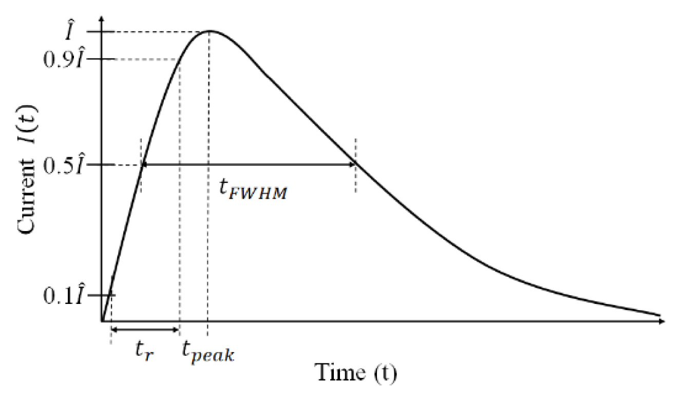
Fig. 1 illustrates a time-domain conducted disturbance noise source defined as a double exponential pulse waveform in the IEC 61000-4-24 conducted disturbance immunity testing standard, as represented by Eq. 1):
Double exponential pulse waveform.
When the current of the double-exponential pulse is positive, the exponential coefficient α should be less than β, as shown in Eq. (2) [18]:
Table 1 lists the various test modes depending on the source pulse requirements presented in the IEC 61000-4-24 standard. Each value of the requirement includes an error, which indicates a specification that the double exponential pulse must satisfy. With a range-based specification, the double exponential pulse can be obtained with a set of design ranges using the proposed design methodology. The pulse parameters are defined as follows:

Conducted early-time HEMP (CEP) source pulse requirements in IEC 61000-4-24 standard
KDE: Modifying factor;
Î: Maximum peak current;
α, β: The characteristic parameters;
tr: The interval of the time required for the leading edge of a pulse to rise from 10% to 90% of the peak pulse amplitude;
tFWHM: The time interval from 0.5Î to half of the maximum peak current Î;
tpeak: The time at the maximum peak current Î.
2. Proposed Equivalent Circuit Model
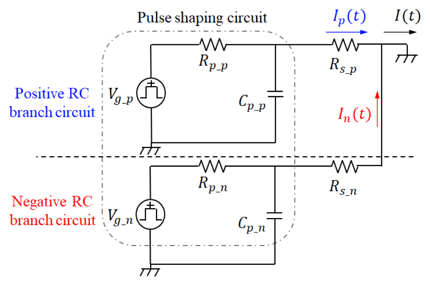
Fig. 2 presents the proposed equivalent circuit model. With step pulse generators, each RC branch circuit generates positive and negative step pulse currents. The circuit components determine the magnitude and time constant of the step pulses to generate a double exponential pulse that satisfies the various source pulse requirements. The definitions of the equivalent circuit components are as follows:
Proposed equivalent circuit model.
Rs: Source impedance resistance;
Rp, Cp: Pulse shaping circuit resistance, capacitor;
Vg: Magnitude of the step pulse generator;
Pulse shaping circuit: Part of the equivalent circuit to determine the time constant and sign of the step pulse;
Underscore p, n: Circuit components belonging to a positive or negative RC branch circuit.
3. Double Exponential Pulse Modeling
To model a double exponential pulse with the proposed equivalent circuit model, the relationship between the output current of the proposed circuit model and the analytical formula of the output current specified in the standard is obtained. The positive and negative step pulse currents generated in each RC branch circuit are defined in Eq. (3). The output pulse current, I(t), can be obtained by combining the two step pulse currents, as expressed in Eq. (4).
where,
As the total current, I(t), converges to zero when it reaches the steady state, as expressed in Eq. (5), the relationship between the magnitude of the step pulses and the resistance of the proposed model is obtained, as expressed in Eq. (6).
Using Eq. (6) with the coefficient comparisons of Eqs. (1) and (4), the relationship between the pulse current, I(t), derived from the proposed circuit and the current equation defined in the standard is determined, as listed in Table 2.

Relationship between source pulse requirements and equivalent circuit model
III. Proposed Design Methodology for Equivalent Circuit Model
In this section, a design methodology for equivalent circuit models is proposed to design various double exponential pulses based on the source pulse requirements. As shown in Fig. 3, two design requirements regarding the source impedance and pulse waveform are employed to determine the equivalent circuit components. The characteristic parameters are key elements in the determination of double exponential pulse characteristics and are modeled using the source pulse requirements in the specified standard. Based on the characteristic parameters, the quantitative ranges of the equivalent circuit components are derived by applying the low-impedance condition for the source impedance and capacitance range for the pulse waveform.
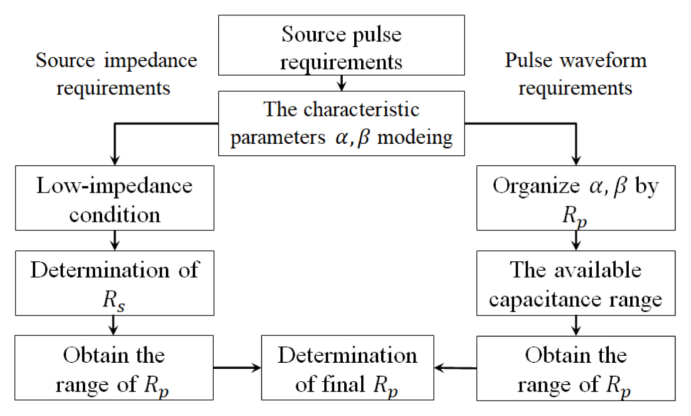
Proposed design methodology.
1. Characteristic Parameter α,β Modeling
To design the equivalent circuit components, the characteristic parameters α,β should first be modeled, because the relationship derived in Table 2 simply defines the correlation with the source pulse requirements and equivalent circuit model, not the characteristic parameters α and β. If the characteristic parameters α and β can be obtained using analytical approaches, the design process of a double exponential pulse can be simplified. However, as the current equation in Eq. (1) is nonlinear, it cannot be solved analytically. In this case, approximation methods for the characteristic parameters, such as Eqs. (7)–(8), are applied. Eqs. (7)–(8) are derived with approximation parameters X and Y, extracted using an iterative approach based on a Nelder-Mead algorithm [21–23].
2. Proposed Equivalent Circuit Model Design Methodology
This section presents two requirements design process of the proposed methodology. By applying this methodology, the ranges of the circuit components corresponding to the design limits of the double exponential pulse, represented by the error in the source pulse requirements, are derived. The designer can then determine the circuit component values according to their design environment within the derived ranges.
1) Source impedance requirement design
As per the standard, the source impedance requirement, Zsource, is defined as a combination of the reference impedance, Zref, and the impedance error, Ze, as indicated in Table 1. The overall output impedance, Zs, of the proposed equivalent circuit model is represented by the parallel synthesis of the impedance of each RC branch circuit, as depicted in Fig. 4.
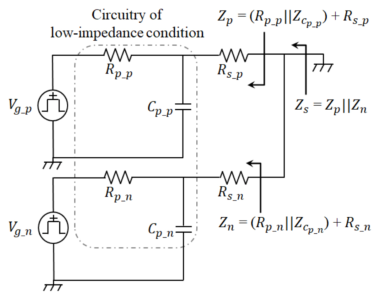
Output impedance of equivalent circuit model.
To match Zsource and Zs, a low-impedance condition limiting the impedance of the pulse shaping circuit composed of Rp and Cp is proposed to approximate the output impedance of double RC branch circuit, Zp and Zn, by two times Zsource. In terms of the impedance value, because the impedance error, Ze, is negligibly small, the impedance of the pulse shaping circuit can be approximated, as shown in Eq. (9), to convert Zp and Zn to 2Zsource.
Assuming that the low-impedance condition is applied because 2Ze is significantly smaller than Rs, the output impedance of one RC branch circuit can be approximated using Rs, as shown in Eqs. (10)–(11).
Subsequently, the source impedance requirements Zsource can be satisfied by determining Rs to 2Zsource, as shown in Eq. (12).
When determining Rs, it should be considered that Zsource has impedance error Ze. Rs should also be set according to Ze because a low-impedance condition should be established even if Zsource changes according to Ze. By applying the impedance error, Ze, in Eq. (9)Rs according to Ze can be obtained using Eqs. (13)–(14).
Rs can be determined using Eqs. (9)–(14), with further analysis of the low-impedance condition being performed to obtain the range of Rp. The low-impedance condition can be described in terms of Rp_p in the positive RC branch circuit, as shown in Eq. (15). In the case of Rp_n of the negative RC branch circuit, the same result was obtained, as shown in Eq. (16).
To solve Eqs. (15)–(16), the parameters B and K are defined, as expressed in Eq. (17). The parameter B indicates the coefficient of inequality and determines the direction of Eqs. (15)–(16). Parameter K is the result of Eqs. (15)–(16) can be replaced by the following equation:
With regard to parameter Bp, Eq. (15) can be expressed in two ways: when Bp is larger than one, Kp is always negative, and the result of the inequality becomes invalid. In the other case, Bp is smaller than one, and the range of Rp_p can be defined using Kp, as expressed in Eq. (18). An identical process can be applied to the negative RC branch circuit to derive the range of Rp_n for Bn and Kn, as expressed in Eq. (19). Depending on the source requirements in the various test modes in the standard, parameter B may be larger than one. In this case, the Rp and Cp pairs that satisfy the low-impedance condition, which is the premise of the source impedance requirement design, can be determined by adopting a repetitive approach.
2) Pulse waveform requirement design
The previously derived relationship presented in Table 2 is re-written in terms of Rp_p and Rp_n, with the characteristic parameters having minimum and maximum values according to the pulse waveform requirements tr and tFWHM, as shown in Eqs. (20)–(21).
To quantify the range of Eq. (20), the available capacitance ranges are employed in the pulse waveform requirement design. The available capacitance ranges are defined as Cp_p_min and Cp_p_max, which are applicable to actual conducted disturbance immunity testing. However, because the capacitance range used to quantify Eq. (20) should be determined by considering all conditions of Cp_p, the available capacitance range is combined with the range of Cp_p, which prevents Rp_p from being negative in Eq. (20). Using the combined capacitance range, Eq. (22) can be derived using Rs_p as a variable in Eq. (20). The same process can also be applied to a negative RC branch circuit to derive the range of Rp_n, as expressed in Eq. (23):
3) Proposed equivalent circuit model design
The proposed equivalent circuit model design methodology combines the results of each requirement design and determines other equivalent circuit components. The range of Rp derived from the combination of each requirement design is defined in Eqs. (24)–(25). When determining the maximum range, a smaller value of each design result should be chosen to minimize the impedance of the equivalent circuit model.
The range of Cp can be determined using the quantified range in Eqs. (24)–(25) and the relationships in Table 2, as expressed in Eqs. (26)–(27).
Once Rs, Rp, and Cp are determined in the obtained ranges, the amplitude of the step pulse generator, Vg, can be estimated using the relationship of Î defined in Table 2 and the boundary condition of the double exponential pulse, as shown in Eqs. (28)–(29).
where
3. Design Example
To validate the proposed equivalent circuit model and the design methodology, a design example is presented using one of the test modes suggested in the IEC 61000-4-24 standard. The design parameters of the equivalent circuit are derived using the proposed design methodology and applied to a circuit simulator to investigate the double exponential pulse designed by the proposed method. The circuit simulation results and the source pulse requirements of the standard are compared to validate the proposed equivalent circuit model and design methodology. The design procedure is the same as that described in Section 3.
Step 1 (The characteristic parameters α,β modeling): The source pulse requirements of the CEP1 test mode and modeled characteristic parameters, α,β, derived from Eqs. (7)–(8) are listed in Table 3. The frequency range applied in the design example is 100 kHz–200 MHz, which is the common HEMP environment frequency range.
Step 2 (Source impedance requirement design): The low-impedance condition is applied, and Rs is determined to be 800 Ω using Eqs. (13)–(14). With the modeled characteristic parameters and the value of Rs, the maximum range of Rp_n is determined to be 30 Ω using Eq. (19), where Kn = 30. In the case of the CEP1 test mode, Bp is larger than one, and the range of Rp_p can be set equal to the range of Rp_n to satisfy the low-impedance condition.
Step 3 (Pulse waveform requirement design): The available capacitance ranges are set to Cp_min = 1 pF, Cp_max = 1 mF. The range of Cp for positive Rp can be calculated using Eq. (20) along with the circuit components in Step 1. The combined capacitance range is determined as 0.13 nF < Cp_p < 1 mF and 1pF < Cp_n < 1 mF. With the determined capacitance range, 0.1 mΩ < Rp_p < 0.5 MΩ and 6.1 μΩ < Rp_n < 0.23 Ω, is obtained from Eq. (19).
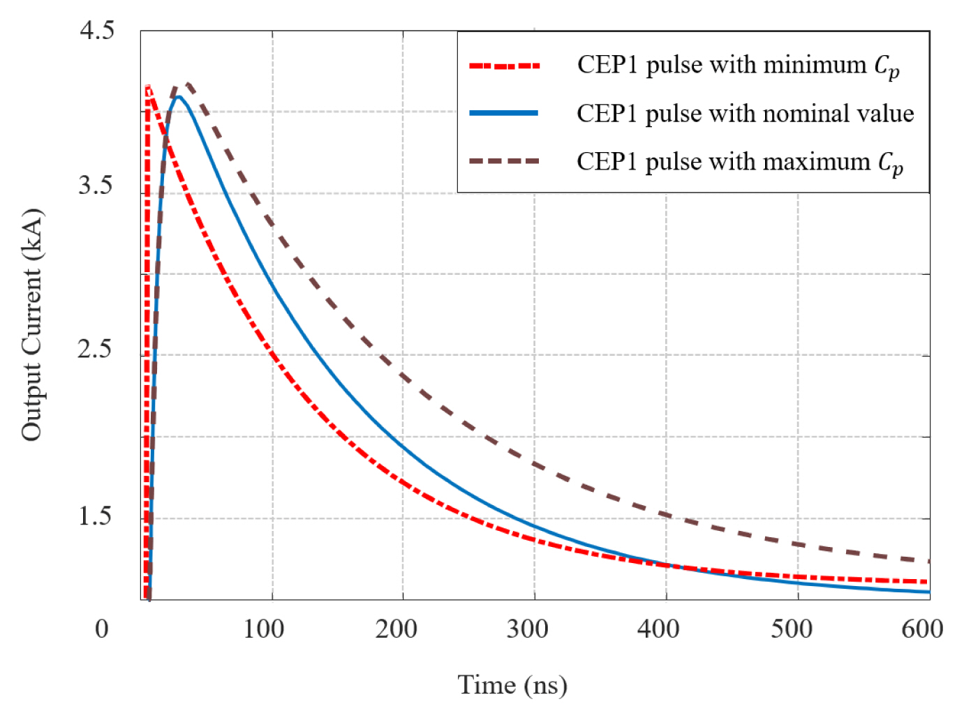
Step 4 (Proposed equivalent circuit model design): The design parameters determined in Step 1 to Step 3 are summarized in Table 4. Circuit simulation is performed with the determined circuit components. In Fig. 5, the pulse waveform characteristics of the generated double exponential pulses vary according to the ranges of Cp obtained using the proposed design methodology. The resistance values, Rp_p and Rp_n, were chosen to be 20 Ohms and 0.2 Ohms, respectively, as nominal values within the range derived in Step 3. Table 5 presents a comparison of the parameters of the source pulse requirements and the circuit simulation results. As presented in Fig. 5 and Table 5, with the proposed equivalent circuit model and design methodology, it is confirmed that it is possible to design a double exponential pulse satisfying the standard error of the source pulse requirements.
IV. Application to Simulation-based Conducted Disturbance Immunity Testing
A simulation-based disturbance testing platform based on the IEC 61000-4-24 standard is employed to validate the proposed equivalent circuit model and design methodology. To configure a simulation-based testing platform, recommendations and requirements in the standard are applied to the testing platform; this includes the minimum separation distance between the ground plane and signal line, the shielding enclosure, 3D electromagnetic modeling of the sensing probe, and the protective device, as shown in Fig. 6 [24]–[27]. The protective device is applied as a ferrite core for testing simplicity. Fig. 7 illustrates the simulation-based conducted disturbance testing platform. The proposed equivalent circuit model of the double exponential pulse generator and the s-parameter symbol of the 3D test setup, which is shown in Fig. 6, are combined to achieve the test platform. A conducted disturbance immunity test is performed along with the double exponential pulse of the CEP1 test mode generated by the proposed design methodology and circuit simulator. As a result of the circuit simulation, the attenuation of the double exponential pulse, defined as a conducted disturbance, is shown in Fig. 8.
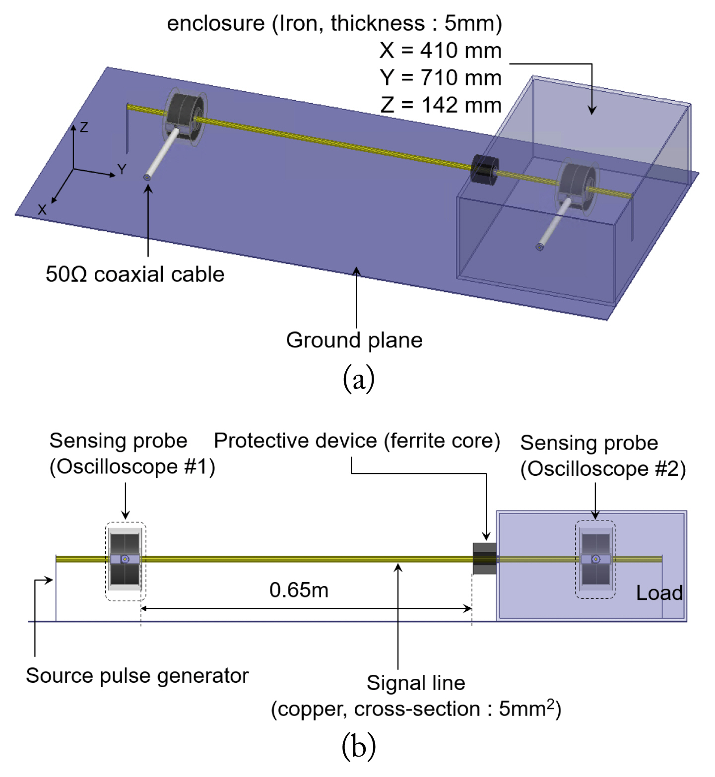
A simulation-based conducted disturbance test setup: (a) trimetric view of test setup and (b) front view of test setup.

A simulation-based conducted disturbance testing platform.
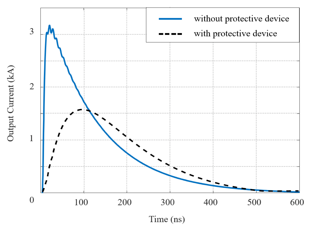
Output double exponential pulse waveform.
Using the simulation results, the validity of the equivalent circuit model of a double exponential pulse generator designed using the proposed method is confirmed.
V. Conclusion
In this paper, an equivalent circuit model and design methodology for a double exponential pulse generator are proposed. The relationship between the source pulse requirements and the equivalent circuit model is derived. A design methodology that determines the feasible value of the circuit components is presented. By applying the proposed design methodology to the equivalent circuit model, a double exponential pulse generator was designed with various test modes required by the disturbance immunity test standards. A simulation-based disturbance immunity-testing platform was configured to validate the effectiveness of the proposed equivalent circuit model and design methodology. It is expected that the immunity of DUTs can be confirmed by the injected noise source in the early design stage with a simulation-based testing platform.
Acknowledgments
The present research has been conducted by the Research Grant of Kwangwoon University in 2021. This work has also been supported in part by the National Research Foundation of Korea (NRF) grant funded by the Korea government (MSIP) (No. NRF-2020R1F1A1065960) and in part by the Institute of Information and Communications Technology Planning and Evaluation (IITP) grant funded by the Korea government (MSIT) (No. 2020-0-00839, Development of Advanced Power and Signal EMC Technologies for Hyper-Connected E-Vehicle, 50%).
References
Biography

Jaesik Moon received the B.S. degree from the Department of Electronics and Communication Engineering at Kwangwoon University, Seoul, South Korea, in 2020. He is also currently pursuing his integrated master’s and Ph.D. degrees at Kwangwoon University. His research interests include system-level electromagnetic compatibility/interference (EMC/EMI) and near-field measurement techniques.

Jong Hwa Kwon received the B.S. degree in E lectronics and Engineering and M.S. degree in Radio Science and Engineering from Chungnam National University, Daejeon, South Korea, in 1994 and 1999, respectively. He received his Ph.D. degree in Electrical and Electronics Engineering from Yonsei University, Seoul, South Korea, in 2010. In January 1999, he joined the Electronics and Telecommunications Research Institute (ETRI), Daejeon, South Korea, where he is currently a principal researcher in the Radio Research Division. He also worked as a visiting scholar at the EMC lab of Missouri University of Science and Technology (MST) from Sept. 2021 to Aug. 2022. His current research interests include theoretical/numerical electromagnetic analysis, EMC/EMP countermeasures and measurement, RFI analysis and countermeasures, and EMC/EMP standards.

Eakhwan Song received the B.S., M.S., and Ph.D. degrees in Electrical Engineering from the Korea Advanced Institute of Science and Technology (KAIST), Daejeon, Korea, in 2004, 2006, and 2010, respectively. In 2010, he was a postdoctoral researcher at KAIST, where he was engaged in high-speed signal integrity and power integrity design in system-in-package as well as equalizer design in high-speed serial links. From 2011 to 2013, he was with the Global Technology Center (GTC), Samsung Electronics, as a senior engineer. At Samsung Electronics, he focused on the design of high-speed serial interconnects and electromagnetic compatibility/interference (EMC/EMI) for ICs, packages, and highly integrated mobile devices. He has been a professor with the Department of Electronics and Communication Engineering at Kwangwoon University, Seoul, South Korea, since 2014. His research interests include system-level EMC/EMI, multigigabit serial interface design, and advanced electromagnetic applications.