I. INTRODUCTION
The recent development of the Internet-of-Things (IoT) has facilitated rapid growth in the smart network systems market, connecting people more effectively than ever before. Specifically, with the increasing popularity of wearable devices in the mobile communication systems market, flexible IoT devices have emerged to play a crucial role in the smart network systems domain. Wearable communication systems have been extensively studied with regard to their various applications. In healthcare systems, wearable communication devices attached to the clothes or bodies of patients enable medical data mining. These devices are also useful in military applications because their lightweight and wearable features increase the mobility of soldiers by reducing the weight and volume of equipment carried by them.
To enable the use of wearable communication devices for such applications, various studies have endeavored to establish wireless communication systems for the flexible IoT market [1–16]. Building such systems requires various wireless communication devices, such as wearable IoT devices, to be flexible [1–11]. To create such flexible IoT devices, the components of radio frequency (RF) devices comprising a wireless communication system need to be highly flexible and exhibit favorable RF characteristics [7–9]. In the early days of research on this topic, solid metals with good RF characteristics, such as gold and copper, were deposited onto flexible substrates to achieve flexibility. However, despite the substrate achieving good flexibility, the poor flexibility of the solid metal caused it to crack easily when the flexible RF device, with a metal layer on a flexible substrate, was folded [7].
Recently, graphene has attracted considerable attention for application in flexible electron devices owing to its flexibility and transparency [1–5]. Specifically, the improved electrical performance of graphene transistors is expected to enable the creation of entirely graphene-based radio frequency integrated circuits (RFIC) for the flexible communication device market [5]. Therefore, in our previous study, we employed graphene for application in RF transmission line [11]. A coplanar waveguide structure was fabricated using a graphene paste layer on a polyethylene terephthalate (PET) substrate, with the former being used as the metal layer due to its good flexibility [11]. However, although the graphene paste/PET structure exhibited good flexibility, its RF characteristics were substantially worse than the structures that used a conventional metal/flexible substrate due to the comparatively low conductance of graphene [11].
Addressing the issues mentioned above, this study developed a graphene-silver nanowire/PET structure, where a graphene-silver nanowire composite film was deposited on the PET substrate to form the metal layer. A silver nanowire is characterized by high electrical conductivity and flexibility, making it a promising candidate for the next generation of conductive thin films [12–16]. In this study, silver nanowire was mixed with graphene at an appropriate ratio to achieve improved flexibility and conductivity. This study specifically investigated the RF loss, conductivity, and skin depth of the graphene-silver nanowire/PET structure with regard to its use in military applications, and subsequently compared these values to those of conventional graphene/PET structures in the X-band.
II. RESULTS AND DISCUSSION
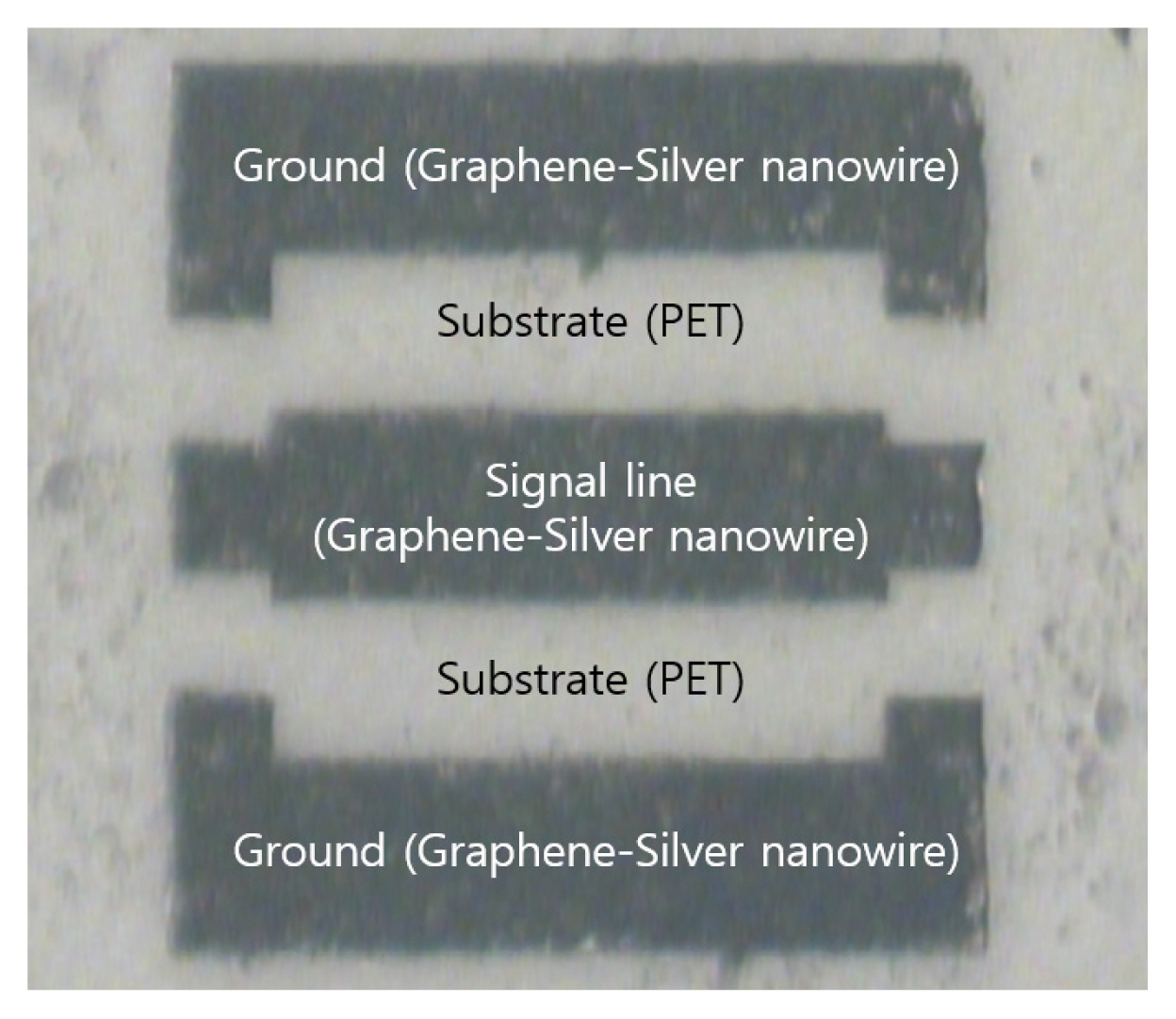
Fig. 1 shows a photograph of the graphene-silver nanowire composite film, where a graphene oxide membrane covers the silver nanowire structure, while the silver nanowires form an interconnected network. This study presumes that the graphene-silver nanowire composite film will exhibit improved electric conductivity due to its use of the silver nanowire network instead of conventional graphene oxide [11]. To compare this structure with the one proposed in our previous study [11], a sample structure having the same size and shape as the structure in our previous study was fabricated. The signal line and ground comprising the graphene-silver nanowire were patterned onto a PET substrate with a thickness of 200 μm. Meanwhile, the thickness of the graphene-silver nanowire film was 2 μm, the width W of the signal line was 150 μm, and the gap between the signal line and the ground was 100 μm.
The circuit of the proposed structure is depicted in Fig. 2. Notably, measurement pads are necessary to perform on-wafer measurements of the transmission line. In such a case, if the widths of the measurement pad and the signal line differ significantly, the resulting discontinuity would make it difficult to measure the loss of the transmission line due to the loss caused by the parasitic component. To reduce such parasitic components in this study, the width of the signal line and that of the measurement pad were kept similar—around 150 μm.
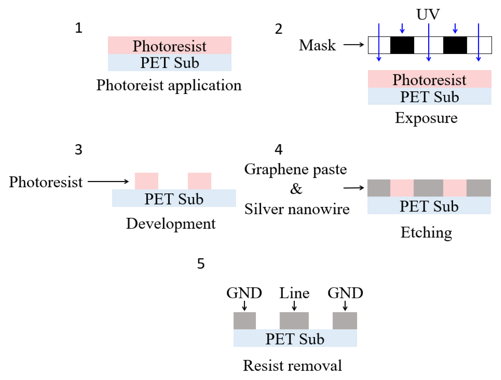
In this context, it must be noted that an increase in the thickness of a graphene-nanowire film leads to a decrease in loss of the transmission line. However, if the film is too thick, the thickness of the photoresist also increases, resulting in imperfect pattern formation during the photoresist removal process in photolithography. Conversely, if the graphene-nanowire film is too thin, the skin effect causes an increase in transmission line loss. Considering these circumstances, the thickness of the graphene-nanowire film that caused the least loss at a possible line in photolithography was found to be 2 μm. As shown in Fig. 3, the coplanar waveguide employing the graphene-silver nanowire structure was fabricated using the photolithography method. First, the PET substrate was thoroughly cleaned using deionized water (DI), following which 15 mL of photoresist (PR) solution (AZ5214E) was spin-coated onto the PET substrate at a rotation speed of 1,000 RPM for 50 seconds. Next, the substrate was subjected to a 1-minute soft baking process on a hotplate at a temperature of 90°C. After aligning the substrate with a mask, it was exposed to UV light for 30 seconds and then immersed in AZ300MIF solution for 2 minutes to remove the PR solution. Upon completion of the development process, a thin layer of graphene silver nanowire paste was applied onto the PET substrate. Following this, a three-minute hard baking process was performed on a hotplate at a temperature of 90°C. Subsequently, the lift-off process was carried out using an ace-tone solution.
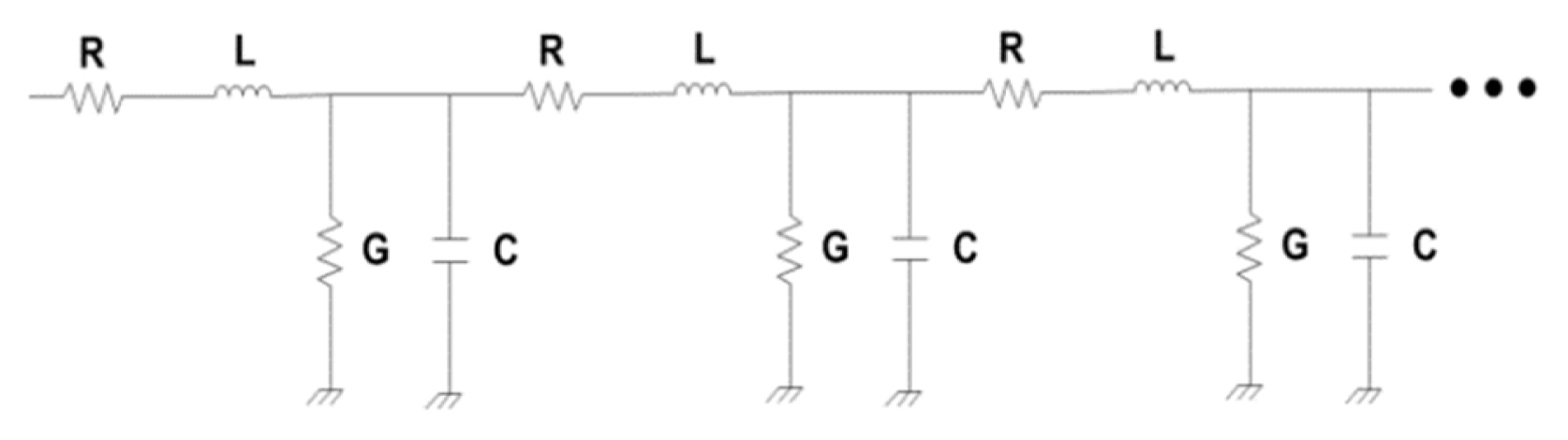
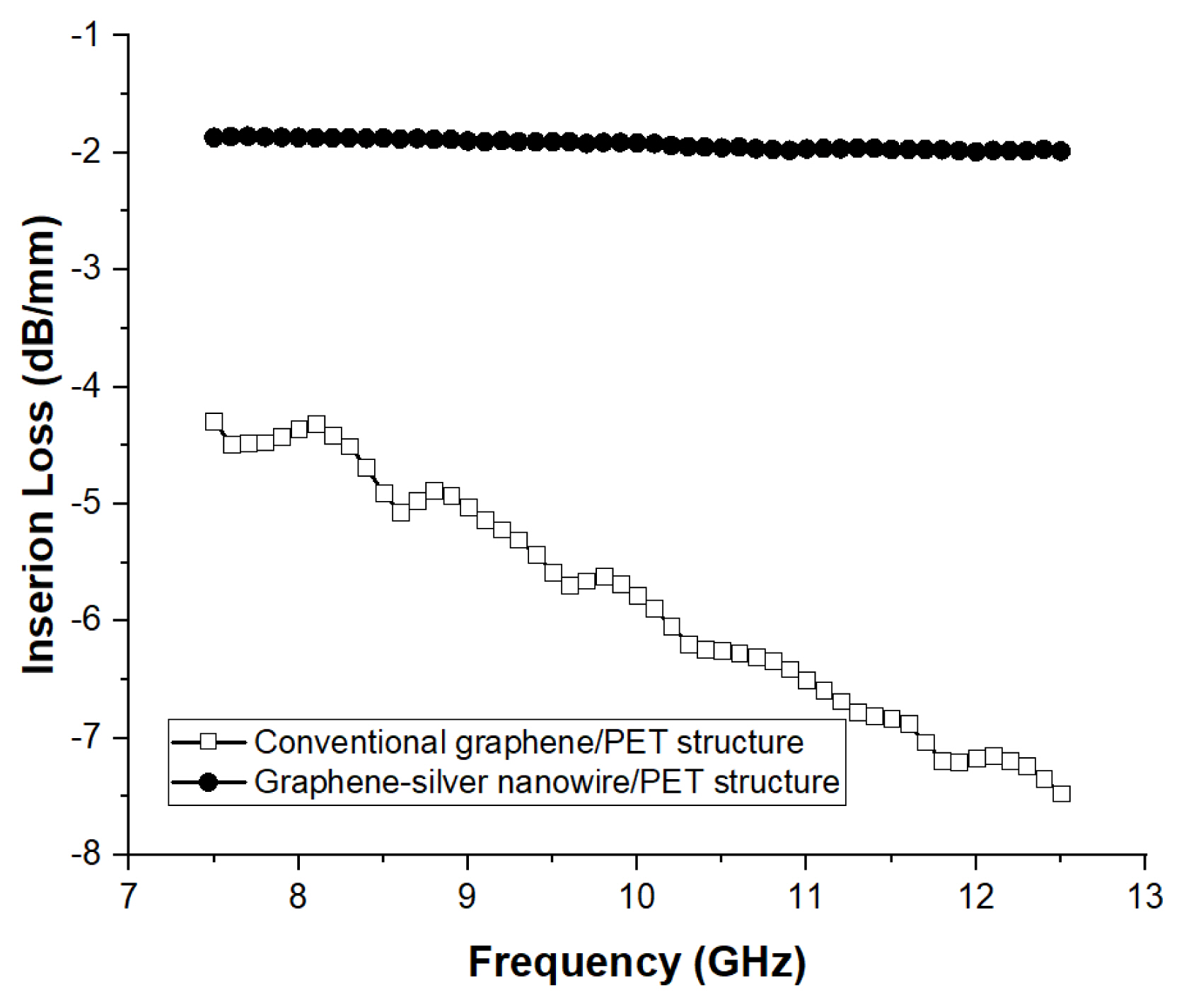
Fig. 4 shows the insertion loss S21 per 1 mm of a coplanar waveguide employing a graphene-silver nanowire/PET structure compared to that employing a graphene/PET structure in the X-band for military applications [11]. To extract the insertion loss, the 50 Ω-based S-parameter (S21) of the transmission line was measured using the on-wafer vector network analyzer. The value was then normalized using the characteristic impedance of the transmission line. Notably, the characteristic impedance of the coplanar waveguide employing the graphene-silver nanowire/PET structure was measured to be 95Ω. Furthermore, the coplanar waveguide employing the graphene-silver nanowire/PET structure showed a lower loss than that employing a conventional structure. Overall, the conventional structure exhibited a maximum insertion loss of −7.47 dB/mm, while the graphene-silver nanowire structure showed a maximum insertion loss of −1.98 dB/mm. Furthermore, the coplanar waveguide employing a graphene-silver nanowire/PET structure displayed significantly lower frequency dispersion characteristics than those employing a conventional graphene/PET structure [11]. This tendency may be attributed to the existence of various propagation modes in the graphene/PET structure, which resulted in a difference in skin depth between the two structures. This tendency will be explained in detail later in this paper.
Fig. 5 traces the attenuation constant α per 1 mm of the coplanar waveguide employing the graphene-silver nanowire/PET structure. Notably, the attenuation constant α was extracted from the insertion loss S21 based on the method explained below.
If an electromagnetic wave propagates on a line with length l, the insertion loss S21 can be expressed as:
Drawing on the above equation, the attenuation constant α can be obtained as follows:
As shown in Fig. 4, the graphene-silver nanowire structure exhibits a lower loss compared to the conventional graphene/PET structure. Furthermore, Fig. 5 demonstrates that the attenuation constant α of the conventional graphene/PET structure is less than 0.86 Np/mm, while that of the graphene-silver nanowire is less than 0.22 Np/mm. The low loss of the graphene-silver nanowire structure is a result of the silver nanowire’s high conductivity. Subsequently, the electric conductivity of the graphene-silver nanowire structure was extracted using the following equation [17]:
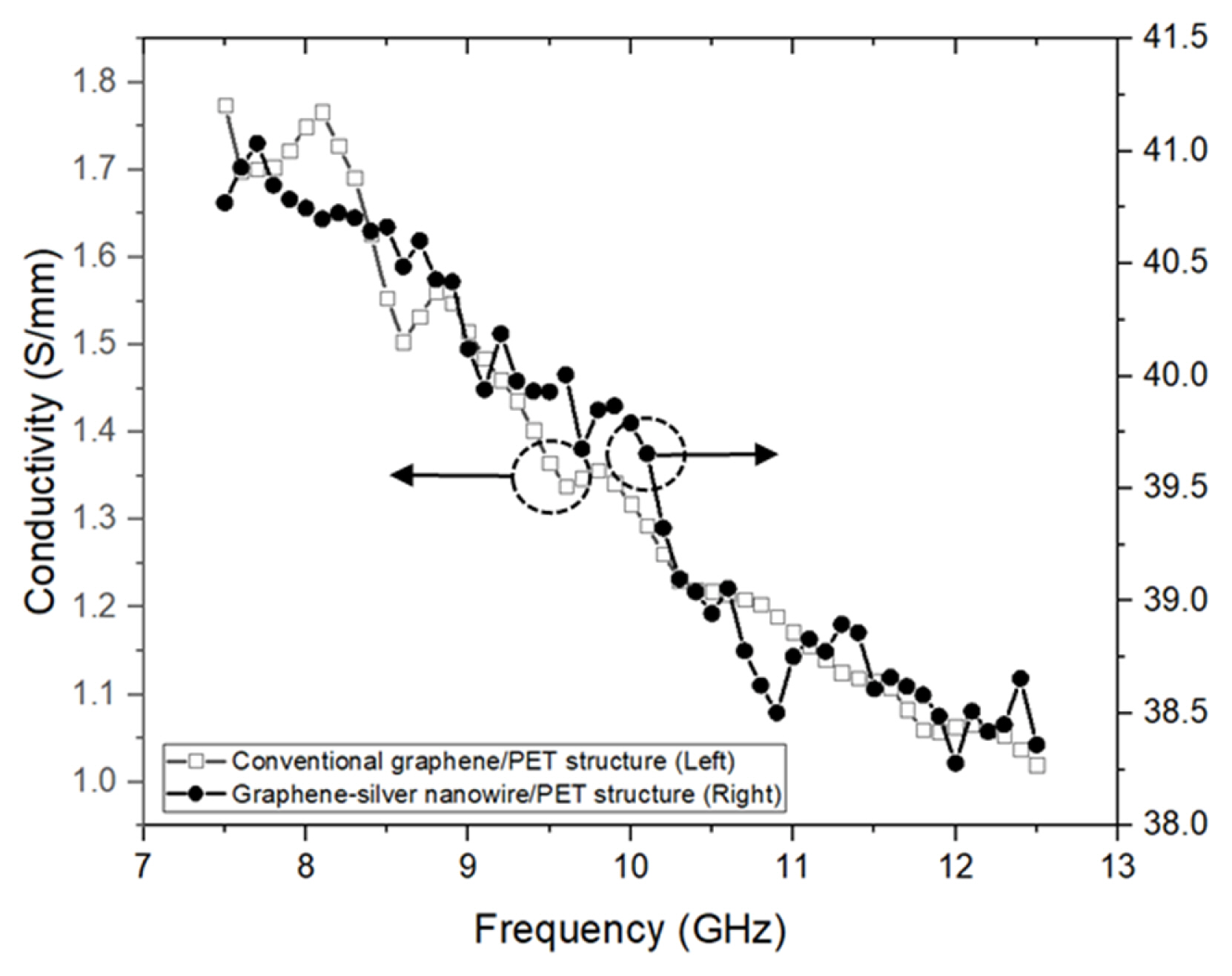
In the above equation, α is the attenuation constant of the structure, Z0 is the characteristic impedance of the transmission line, and w and t indicate the width and thickness of the signal line, respectively. Fig. 6 shows the electric conductivity σ per 1 mm of the graphene and the graphene-silver nanowire, values for which were extracted using Eq. (3), where the latter displays substantially higher conductivity values than the former. While the graphene-silver nanowire/PET structure shows conductance values of 38.66–40.77 S/mm in a frequency range of 7.5 GHz–12.5 GHz, the values for the conventional graphene/PET structure are 1.01–1.77 S/mm in the same frequency range. Notably, the low conductance value of the graphene layer induces high resistance. Therefore, unlike a perfect conductor, a part of the electromagnetic wave penetrated into the graphene layer of the graphene/PET structure due to the layer’s large skin depth, which induced various modes of electromagnetic wave propagation, as well as the quasi-transverse electromagnetic (quasi-TEM) mode [17]. These various modes of electromagnetic wave propagation resulted in strong frequency dispersion characteristics, as shown in Figs. 4 and 5. Meanwhile, in the proposed graphene-silver nanowire/PET structure, electromagnetic wave propagation occurred along the surface of the graphene-silver nanowire due to the latter’s relatively low skin depth, while a dominant quasi-TEM mode was observed on the graphene-silver nanowire/PET structure, resulting in a weak frequency dispersion characteristic, as shown in Figs. 4 and 5.
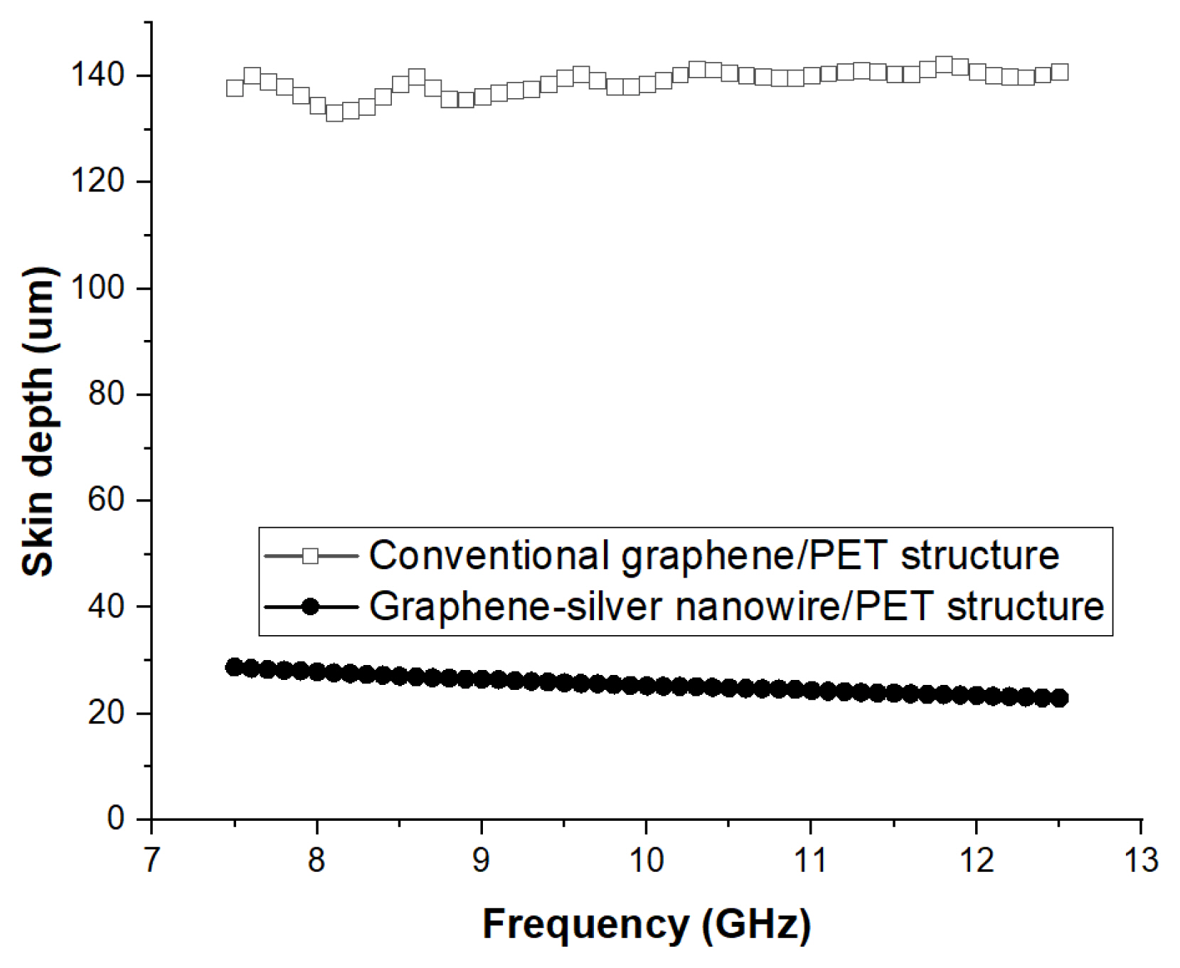
Fig. 7 illustrates the skin depth of the two structures, extracted using the following equation:
In the above equation, ω is the angular frequency, while μ and σ represent the permeability and conductance of the signal line, respectively. As shown in Fig. 7, the skin depth of the conventional graphene/PET structure at 12.5 GHz is 140.96 μm, while that of the graphene-silver nanowire/PET structure is 22.98 μm. These results indicate that the coplanar waveguide employing a graphene-silver nanowire/PET structure is suitable for broadband applications due to its significantly weak frequency dispersion characteristics.
Table 1 presents the changes in electrical conductivity according to the modifications in the mixing ratio of silver nanowires and graphene paste. It is evident that as the mixing ratio of the silver nanowires gradually increases, the conductivity of the graphene-silver nanowire film increases along with it. This change can be attributed to the higher ratio of silver nanowires, which indicates a higher density of such nanowires in the composite film, resulting in adjacent nanowires arranged closer to each other in the silver nanowire network. Therefore, as the ratio of the silver nanowires increases, it becomes increasingly difficult for electromagnetic waves to penetrate the graphene-silver nanowire film, effectively resulting in a lower skin depth of the electromagnetic wave and higher conductivity of the graphene-silver nanowire film. Therefore, as shown in Table 1, the conductivity of the graphene-silver nanowire structure is enhanced by gradually increasing the ratio of silver nanowires.
Table 2 shows that the transmission line proposed in this paper experiences lower losses compared to other graphene-based transmission lines—a phenomenon that can be attributed to the excellent conductivity of silver nanowires [18–20].
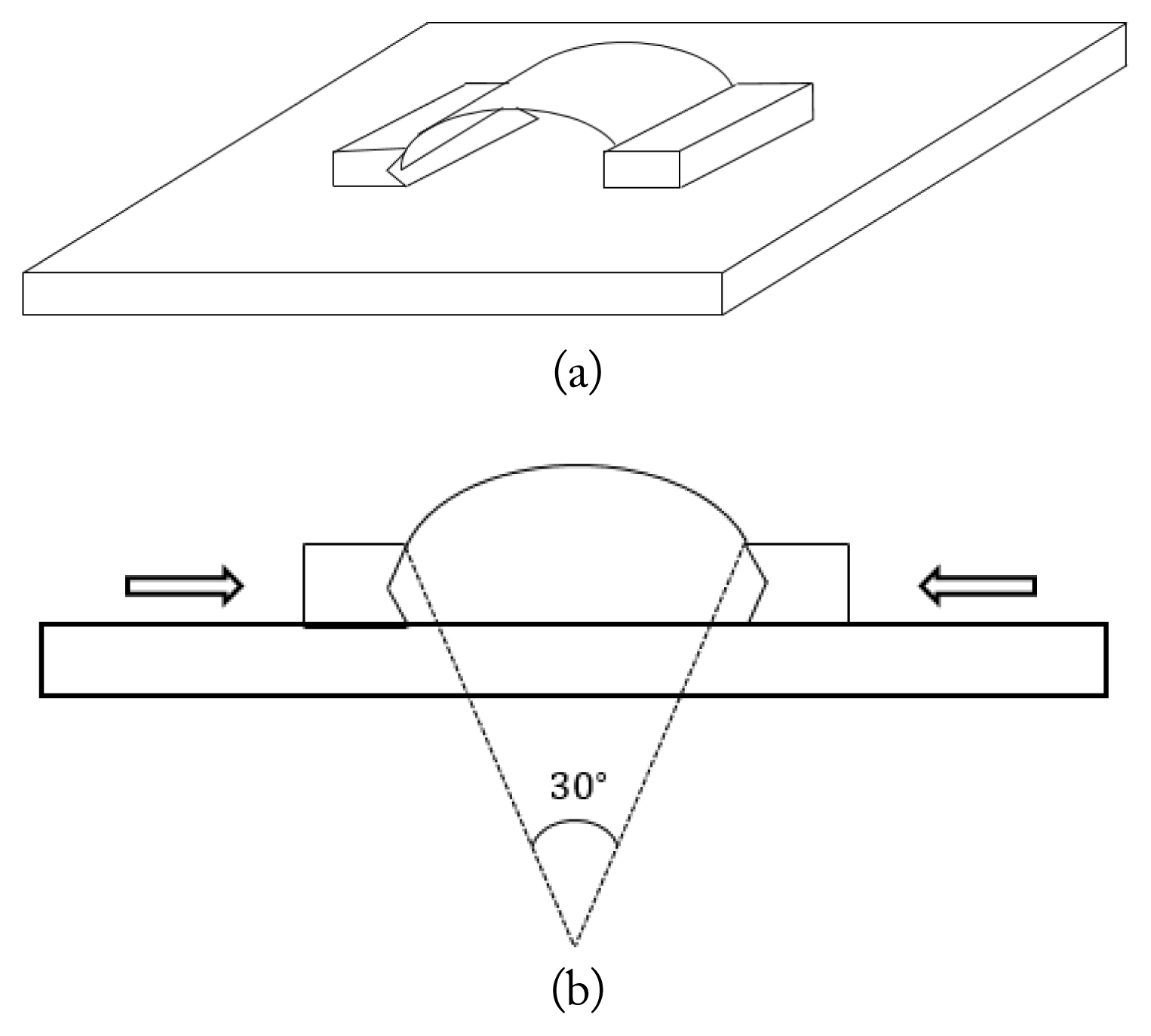
Devices used in flexible wireless communication systems must maintain mechanical and electrical stability in addition to high RF characteristic. In other words, flexible devices should feature reproducibility in electrical performance, even when they are folded multiple times. Therefore, a bending test was performed to confirm the presence of electrical stability in the graphene-silver nanowire in repetitive bending circumstances. As shown in Fig. 8, the graphene-silver nanowire/PET structure was bent at an angle of 30° before the test since wearable devices attached to military uniforms bend slightly at a maximum angle of 30° when soldiers move.
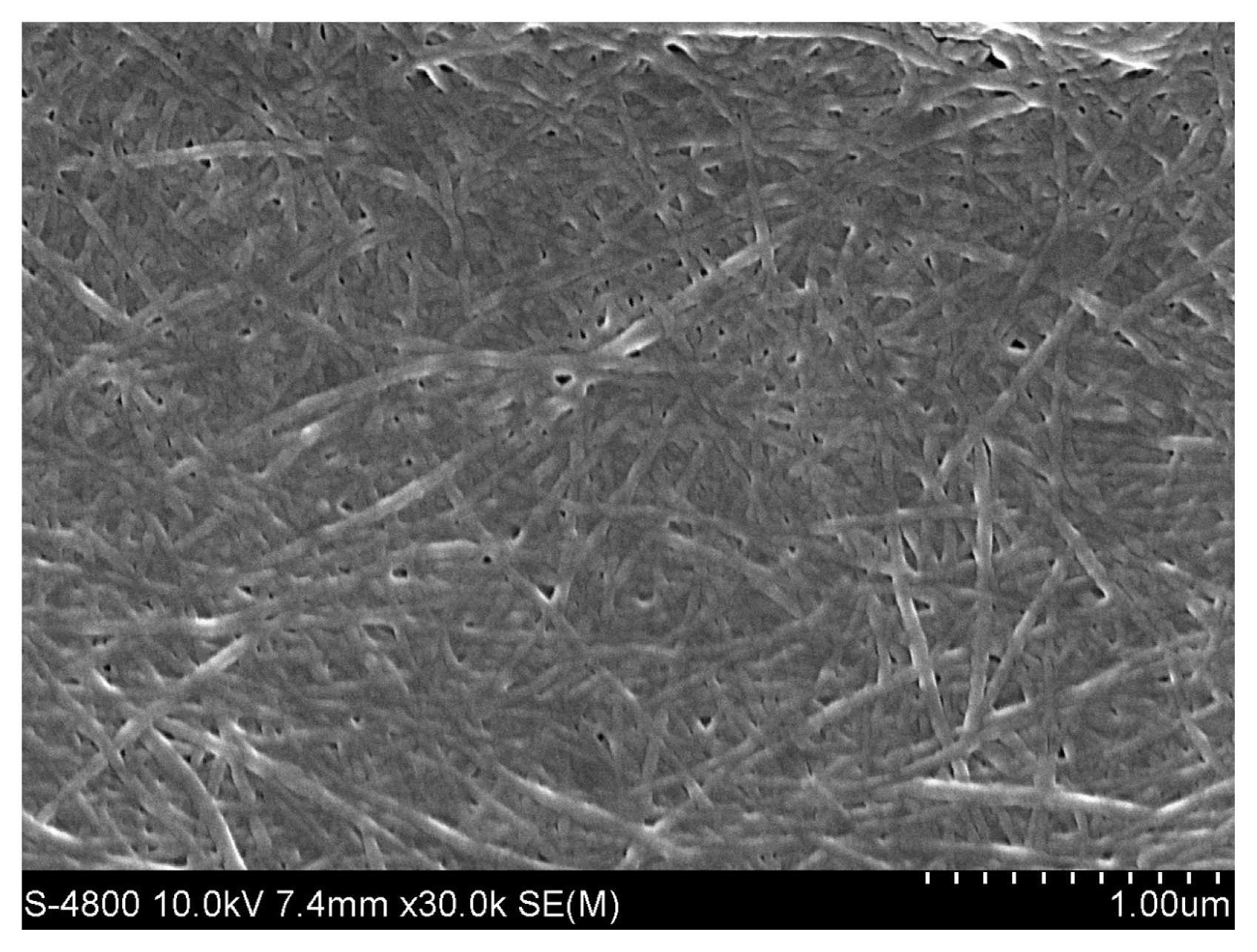
The results obtained in previous studies have shown that a gold/PET structure cracks easily when it is folded due to its insufficient flexibility, thus making it impossible to conduct a bending test [7]. In contrast, the bending test for the graphene-silver nanowire/PET structure could be easily performed due to the structure’s good flexibility. Fig. 8 shows the changes in resistance exhibited by a conventional graphene/PET structure and the proposed graphene-silver nanowire/PET structure when subjected to a bending test. So far, solid metals, such as gold and copper, have been deposited on flexible substrates to realize RF signal lines [7–9]. However, owing to their insufficient flexibility, these metals cracked easily when the flexible RF device was bent [7–9]. In the current study, a bending test was performed on the graphene-silver nanowire/PET structure to investigate its electrical and mechanical stability when it is bent. Specifically, the change in resistance of the graphene-silver nanowire/PET structure was verified by bending it multiple times, as shown in Fig. 8. Furthermore, Fig. 9 shows the change in resistance of the graphene-silver nanowire/PET structure after the bending test, where R1 is the resistance before bending and R2 is the resistance after it was folded. Furthermore, the x-axis refers to the number of bends, and the y-axis represents the ratio of R1/R2. As shown in Fig. 9, the graphene-silver nanowire/PET structure exhibits significantly better electrical stability compared to the conventional graphene/PET structure. In addition, the table shows that the ratio of R1/R2 for the graphene-silver nanowire/PET structure remains less than 1.2 until it is bent 70 times, while it reaches 1.375 after the structure is bent 100 times. Meanwhile, the ratio of R1/R2 for the convenional graphene/PET structure showed a value higher than 2.0 after it was bent only 23 times, further reaching 5.7 after it was bent 100 times. The significantly better electrical stability exhibited by the graphene-silver nanowire/PET structure can be attributed to its silver nanowire network. According to previous studies, a silver nanowire network incurs less damage even when subjected to repetitive bending because the graphene is protected by a well-covered silver nanowire network [15, 16]. Fig. 10 shows a field emission scanning electron microscopy (FE-SEM) photograph of the graphene-silver nanowire structure, where the surface of the coplanar waveguide structure is covered by silver nanowires. According to previous research [15, 16], the protection offered to the graphene by a well-covered silver nanowire network results in highly improved electrical and mechanical stability. However, if the ratio of silver nanowire in a graphene-silver nanowire composite film is higher than 80%, an additional fabrication process would be necessary to achieve sufficient adhesion between the composite film and the PET substrate to address the poor roughness and adhesive properties of the silver nanowire. Therefore, an 80% ratio of the two components (graphene vs. silver nanowire, 2:8) was considered in this study to investigate the RF characteristics.
Although the proposed structure is yet to be sufficiently developed for application in commercial wearable devices, this research makes a meaningful contribution by suggesting the use of a graphene-silver nanowire structure as a solution to the difficulties encountered in realizing graphene-based wearable RFIC.
III. CONCLUSION
This study fabricated a coplanar waveguide employing a novel graphene-silver nanowire/PET structure and investigated its RF characteristics. The proposed structure exhibited lower loss in the transmission line than a conventional graphene/PET structure. Overall, the proposed structure exhibited a maximum insertion loss of −1.98 dB/mm in the frequency range of 7.5–12.5 GHz, compared to the conventional graphene/PET structure that managed a maximum insertion loss of −7.47 dB/mm in the same frequency range. In addition, the graphene-silver nanowire/PET structure showed relatively better frequency dispersion characteristics due to its very low skin depth, originating from its relatively higher conductance. The proposed structure showed conductance values of 38.66–40.77 S/mm in a frequency range of 7.5–12.5 GHz, while the conventional graphene/PET structure exhibited conductance values of 1.01–1.77 S/mm in the same frequency range. Furthermore, the skin depth of the proposed structure was 22.98 μm at 12.5 GHz, while that of the conventional graphene/PET structure was 140.96 μm at the same frequency. During the bending test, the proposed structure showed highly improved electrical and mechanical stability compared to the conventional structure. Apart from this, changes in the resistance of the proposed structure were found to be less than 20% until it was bent 70 times. In contrast, the resistance of the conventional graphene/PET structure changed by more than 100% after it was bent only 23 times. Therefore, according to the results of the bending test, the silver nanowire network sustains less damage even with repetitive bending, since the graphene is protected by a well-protected by silver nanowire network. In conclusion, although the proposed structure is not yet ready for application in commercial wearable devices, this research contributes significantly to the field by proposing the use of graphene-silver nanowire structures as a solution to the obstacles preventing the realization of graphene-based wearable RFIC.