I. INTRODUCTION
The massive multiple input multiple output (MIMO) system is a key element in fifth-generation (5G) communications [1]ŌĆöa technology that is currently used in commercial services based on sub-6 GHz frequencies. The massive MIMO antenna can be deployed on the basis of specific use cases, such as in rural, urban low-rise, and dense urban scenarios [2]. Moreover, the total number of subarrays and antennas can also be changed according to the use scenarios. For example, since a dense urban scenario requires expansive vertical coverage for multi-user MIMO, two subarray antennas along with 64T64R or 64 radio chains can be deployed. Frequency bands for 5G new radio are usually separated into two different frequency ranges, FR1 and FR2 [3]. FR1 includes sub-6 GHz frequency bands, which have been frequently used by previous standards. FR1 covers potential new spectrum offerings from 410 MHz to 7,125 MHz and involves frequency division duplexing (FDD) bands, such as PCS (uplink 1,850ŌĆō1,910 MHz; downlink 1,930ŌĆō1,990 MHz) and AWS (uplink 1,710ŌĆō1,780 MHz; downlink 2,110ŌĆō2,180 MHz). This study proposes a dual-band (PCS and AWS bands) base station antenna that can provide massive MIMO technology and can be deployed with an extension of more than 16T16R or 16 radio chains.
However, the introduction of massive MIMO technology has made it more difficult to implement the antenna due to size constraints. Given that the elements of an antenna are usually situated close to each other, mutual coupling between these elements is often inevitable. Specifically, a wideband FDD antenna is more prone to suffering more severely due to such a problem, since the distance between its elements is usually very small. The massive MIMO antenna must also obtain polarization characteristics, such as input ports isolation and cross-polarization discrimination (XPD) with a subarray configuration. In the case of dual-polarized antennas, several efforts have been made to improve their input port isolation and XPD [4ŌĆō7]. In this context, a single dual-polarized quadruple L-probe patch antenna can achieve good isolation performance using broadband baluns deployed in a dual-feed configuration. However, a subarray antenna configuration is more widely used for high gain achievement [2]. Notably, the use of the dual-feed method is difficult to implement in subarray antennas when there is limited area available.
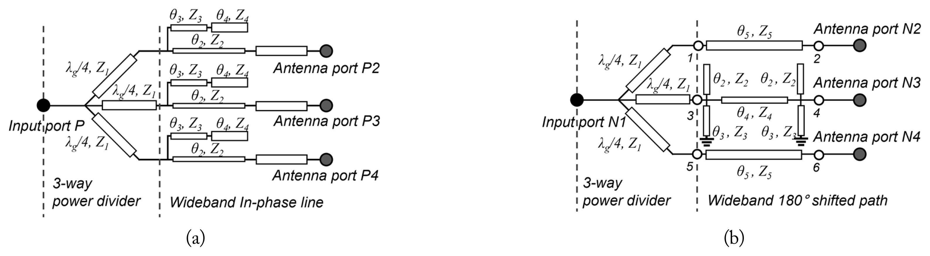
This study proposes a compact 1:3 power divider with a 180┬░ shifted path, as shown in Fig. 1(a) and 1(b), to ensure polarization purity over a wide bandwidth. A center-positioned element of a three-subarray antenna is physically rotated at a 90┬░ angle to change the current distribution of the patch antenna so as to achieve reduced port-to-port mutual coupling and enhanced polarization purity [8]. Notably, the proposed structure is able to offer both XPD and isolation while maintaining considerable bandwidth and beam performance. In addition, the proposed antenna array exhibited competent passive inter-modulation (PIM) performance. Generally, inter-modulation occurs when two RF signals are mixed in nonlinear devices. If this nonlinearity is caused by passive devices, such as antennas and connectors, the resulting inter-modulation is called PIMŌĆöa crucial issue in the FDD system that has persisted despite the use of filters [9, 10]. PIM can create interference and decrease receiver sensitivity. To address this, a floating metal wall was utilized in the proposed antenna array to reduce mutual coupling between the antenna arrays and, in turn, to maintain PIM performance. Moreover, it contributes to attaining column beam performance, including beam width and XPD.
II. FEEDING NETWORK CONFIGURATION
1. The 1:3 Power Divider Design
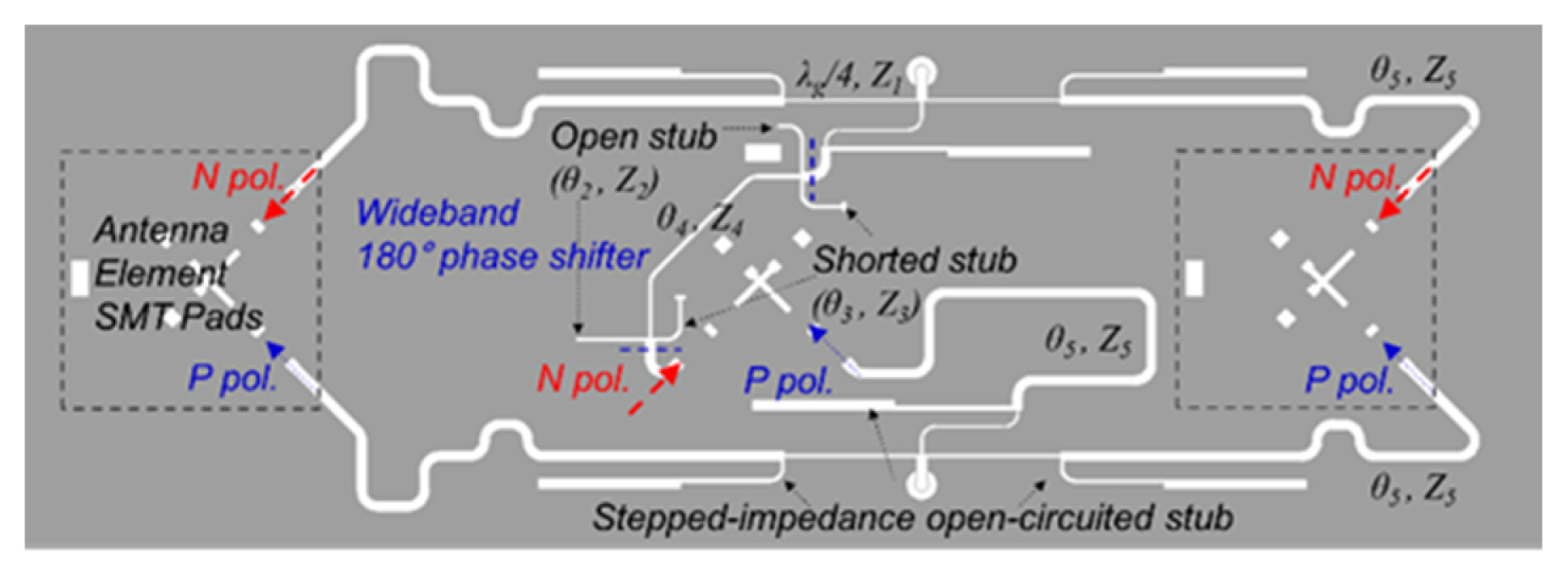
The proposed compact 1:3 power divider, comprising wideband in-phase transmission lines with stepped-impedance open-circuited stubs, is illustrated in Fig. 1(b). To ensure equal power splitting, the impedance of the quarter-wavelength lines must be Z1 = Z0 ├Ś ŌłÜ3 = 86.6 ╬® [11]. A simulation model of the in-phased 1:3 power divider is presented in Fig. 2, where +45┬░ polarization (P-pol.) of the dual-polarized antenna arrays were fed with symmetrical power dividers. While stepped-impedance open-circuited stubs were introduced to achieve wideband characteristics [12], they may also be used to generate additional transmission poles to attain better impedance matching in wide bandwidths.
Fig. 1(b) presents a schematic of the compact 1:3 power divider with a 180┬░ shifted path [13, 14]. The structure consists of parallel open-circuited and short-circuited stubs. In contrast to other wideband phase shifters, such as the Schiffman phase shifters [4], these stubs can be compactly implemented.
Fig. 2 illustrates the simulation model of the proposed 1:3 power divider, as realized in a restricted space. The scattering parameters of the wideband 180┬░ phase shifter presented in Fig. 1(b) are derived as (1)ŌĆō(4) [11ŌĆō14], as noted below:
(3)
(4)
From the above equations, ╬Ė4 = ŽĆf╠ä, ╬Ė2 = ╬Ė3 = 0.25ŽĆfŽå, ╬Ė5 = [ŽĆ + ╬öŽåT(f0)] fŽå was achieved.
2. VERIFICATION OF THE DESIGN
The 1:3 power dividers illustrated in Fig. 2 were simulated and fabricated using a low-loss FR-4 substrate with ╔ør = 3.52, tan╬┤ = 0.004, and thickness = 0.8 mm. The simulation to achieve wide bandwidth and phase characteristics was performed using Ansys Software. Once the printed circuit board (PCB) was fabricated, each port was connected and measured using SMA-type connectors.
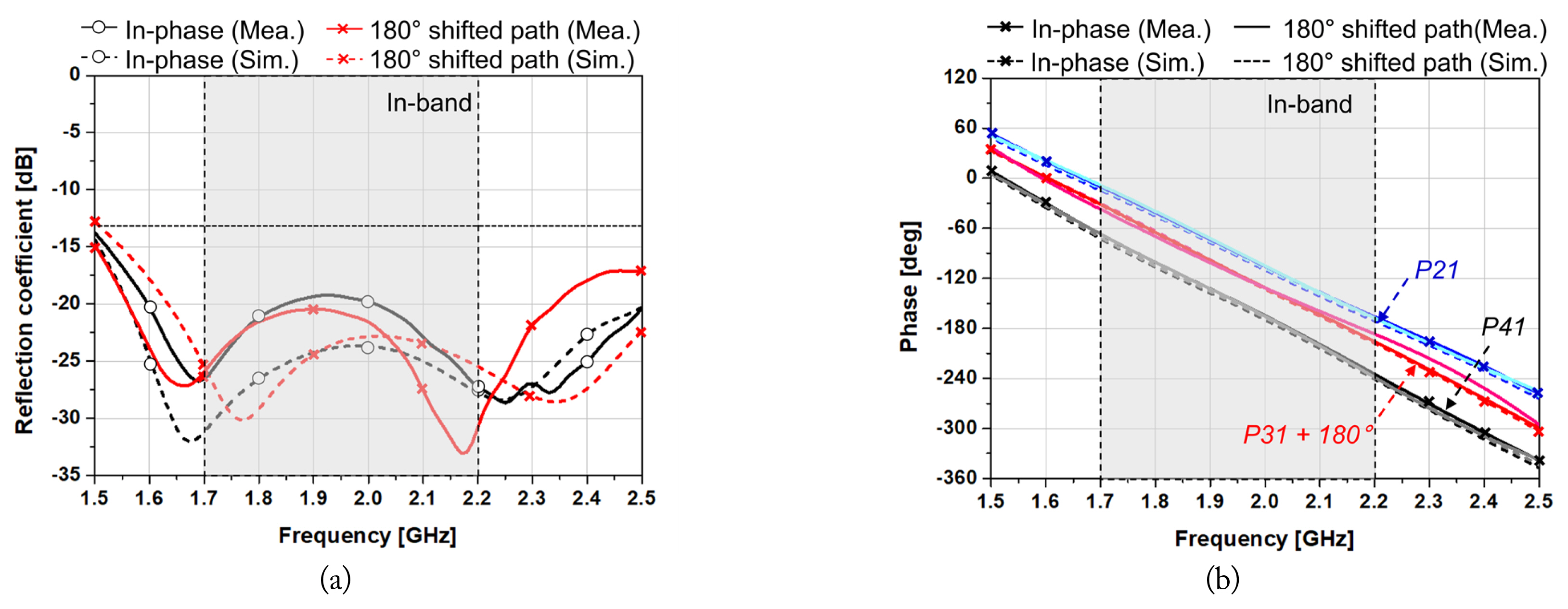
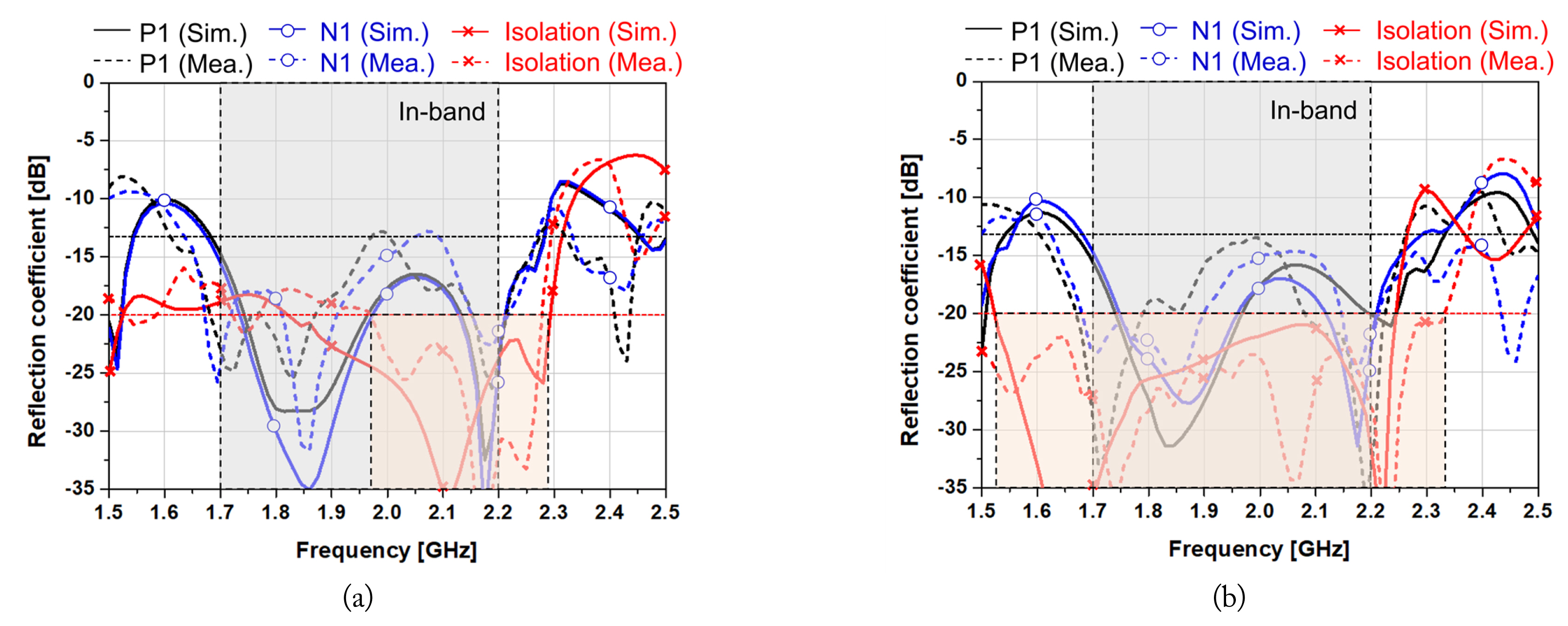
Fig. 3 compares the simulated and measured results, with Fig. 3(a) plotting the reflection coefficients of the in-phase power divider (P1) and the 180┬░ shifted path (N1), measured at input port 1. Although both measured results are higher than the simulated results, the values indicate a wide bandwidth with a ŌłÆ13 dB specification. Fig. 3(b) plots the phases of the two power dividers, with their values measured from input port 1 to antenna ports 2, 3, and 4. The phases of the three ports were designed to maintain a 30┬░ difference so as to achieve a 6┬░ down-tilted subarray elevation beam pattern. To compare the results, 180┬░ was added to the P31 of the power divider with a 180┬░ phase shifted path. The results show that the phase differences of the two paths are almost similar, displaying consistent results over considerably wide bandwidths.
III. Antenna Design and Configuration
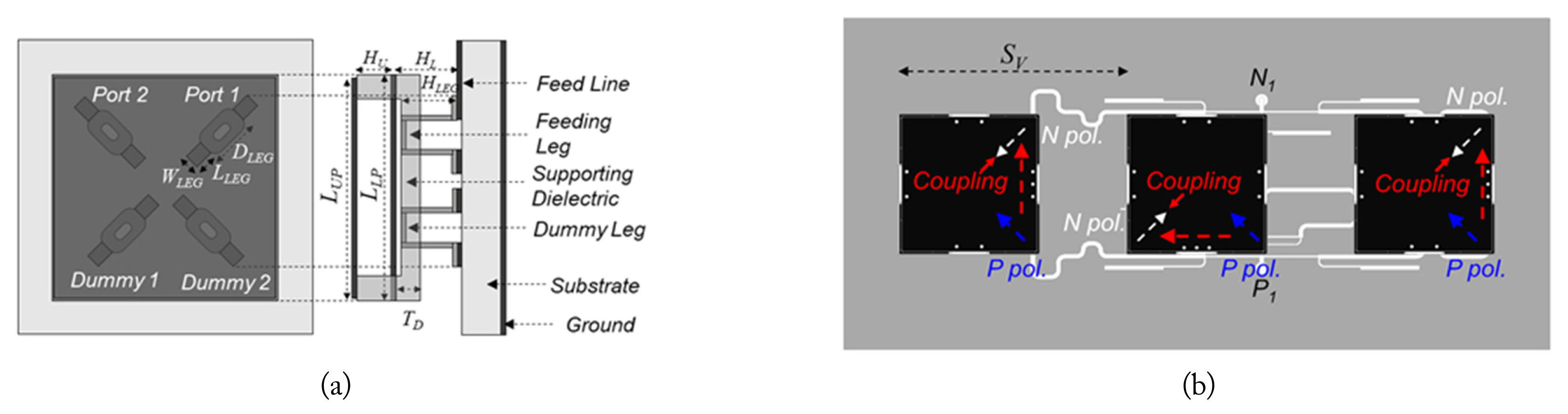
Fig. 4(a) presents a dual-polarized quadruple ╬Ā-probe feed stacked patch antenna element designed to attain wide bandwidth, high XPD, and high isolation between input ports. The ╬Ā-shaped legs help to improve performance and can be used to affix the antenna element on a PCB. Moreover, dummy legs can enhance the polarization purity and tensile strength of the element. The three-subarray antenna simulation model is illustrated in Fig. 4(b). As mentioned previously, a center-positioned element is physically rotated to attain a 180┬░ angle, and the wideband 180┬░ phase shifter is adapted to maintain antenna polarization. Polarization characteristics, such as XPD and isolation, can be enhanced by changing the cross-polarized components of the center element by rotation [8]. The excitation enables their probe leakage radiation to mutually cancel out the leakage radiation of adjacent elements.
The square patches, with LLP = 55 mm, LUP = 54 mm, HL = 12 mm, HU = 8 mm, and thickness = 2 mm, are situated on the supporting dielectricŌĆöa liquid crystal polymer (LCP) with ╔ør = 3.86, tan╬┤ = 0.0023, and TD = 2 mm. The parameters of the ╬Ā - probe feeders are HLEG = 11 mm, DLEG = 6 mm, LLEG = 1.5 mm, WLEG = 2 mm, and thickness = 0.5 mm. The dimensions of the dummy legs were consistent with those of the feeding legs. Subsequently, the positions of both kinds of legs were adjusted to achieve better bandwidth and isolation. The ground size of the three-subarray antenna presented in Fig. 4(b) is 79 mm ├Ś 273 mm, while its horizontal array spacing is 79 mm (0.56╬╗0 at 2.11 GHz) and vertical array spacing (SV) is 91 mm (0.64╬╗0 at 2.11 GHz).
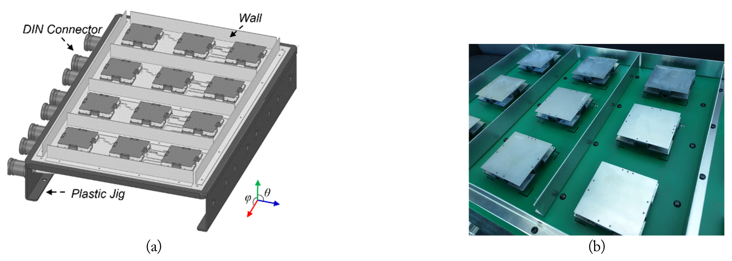
Generally, plastic injection molding and SMT processes are used for the mass production of antenna arrays. The injection molding process can be used to fix the legs of the antenna to designated positions in a supporting dielectric, while patches can be fixed by welding. This study uses LCP as the supporting dielectric, as it has heat-resistant properties that can help withstand the high temperatures during the SMT process. The fabrication of the 3 ├Ś 4 antenna array model, which includes a plastic jig, DIN connectors, and metal walls, is shown in Fig. 5(a). Fig. 5(b) shows a photograph of the fabricated sample. The plastic jig and DIN connectors were used to ensure accurate measurements of the PIM values, while the metal walls were used to adjust the column beam widths and enhance isolation between the subarrays (S21). These floating walls were fixed using plastic rivets to prevent them from affecting the PIM values.
IV. ANTENNA PERFORMANCE
Fig. 6 presents a comparison of the reflection coefficients of the three-subarray antenna. Fig. 6(a) presents the results obtained when using an in-phase power divider, while Fig. 6(b) gives the results attained using a wideband phase shifter, as shown in Fig. 2. Both results exhibit impedance bandwidths of approximately 30% (P1, N1 < ŌłÆ13 dB), ranging from 1.68 GHz to 2.25 GHz. Similar bandwidths were observed on introducing the stepped-impedance open-circuited stubs into the designs. Fig. 6 also compares the isolation between the P1 and N1 of the three-subarray antenna. The results obtained using an in-phase power divider show isolation bandwidths of approximately 14% (<ŌłÆ20 dB), ranging from 1.98 GHz to 2.28 GHz, which are higher than the specifications in the operating band. On employing the wideband phase shifter, the same antenna elements exhibit wider isolation bandwidths of approximately 43% (<ŌĆō20 dB), ranging from 1.5 GHz to 2.33 GHz. These results satisfy the specifications of the operating band, indicating the effects of the proposed design.
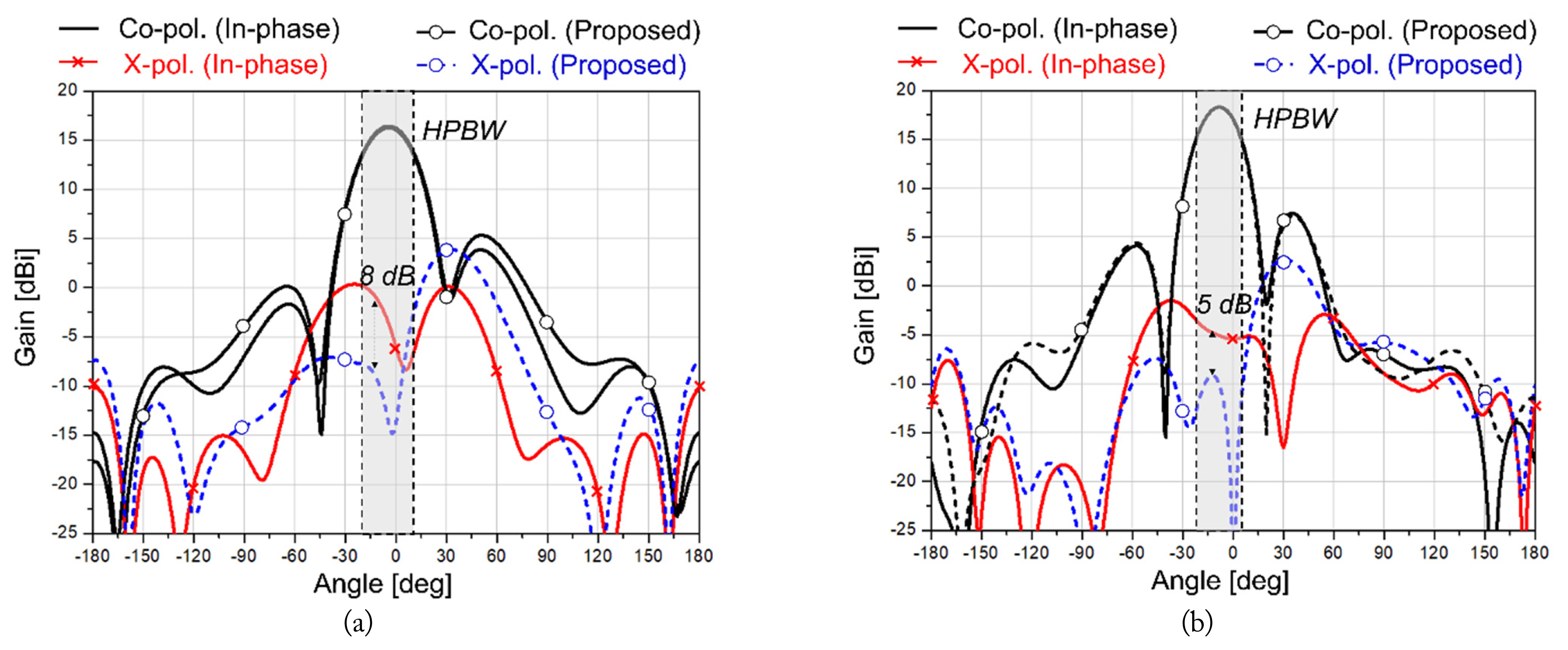
The difference in radiation patterns of the antenna array using the in-phase power dividers and the proposed array are presented in Fig. 7, with the elevation beam patterns of the 3 ├Ś 4 antenna array at each operating band plotted in Fig. 7(a) and 7(b). The results show 15.5 and 18.5 dBi peak gains at each frequency. Furthermore, the half-power beam widths (HPBW) are approximately 30┬░ and 20┬░ at each frequency. On using a wideband 180┬░ shifted path, the cross-polarization (X-pol.) in the HPBW was observed to be suppressed at every frequency, while the XPD increased by approximately 8 dB and 5 dB at each frequency.
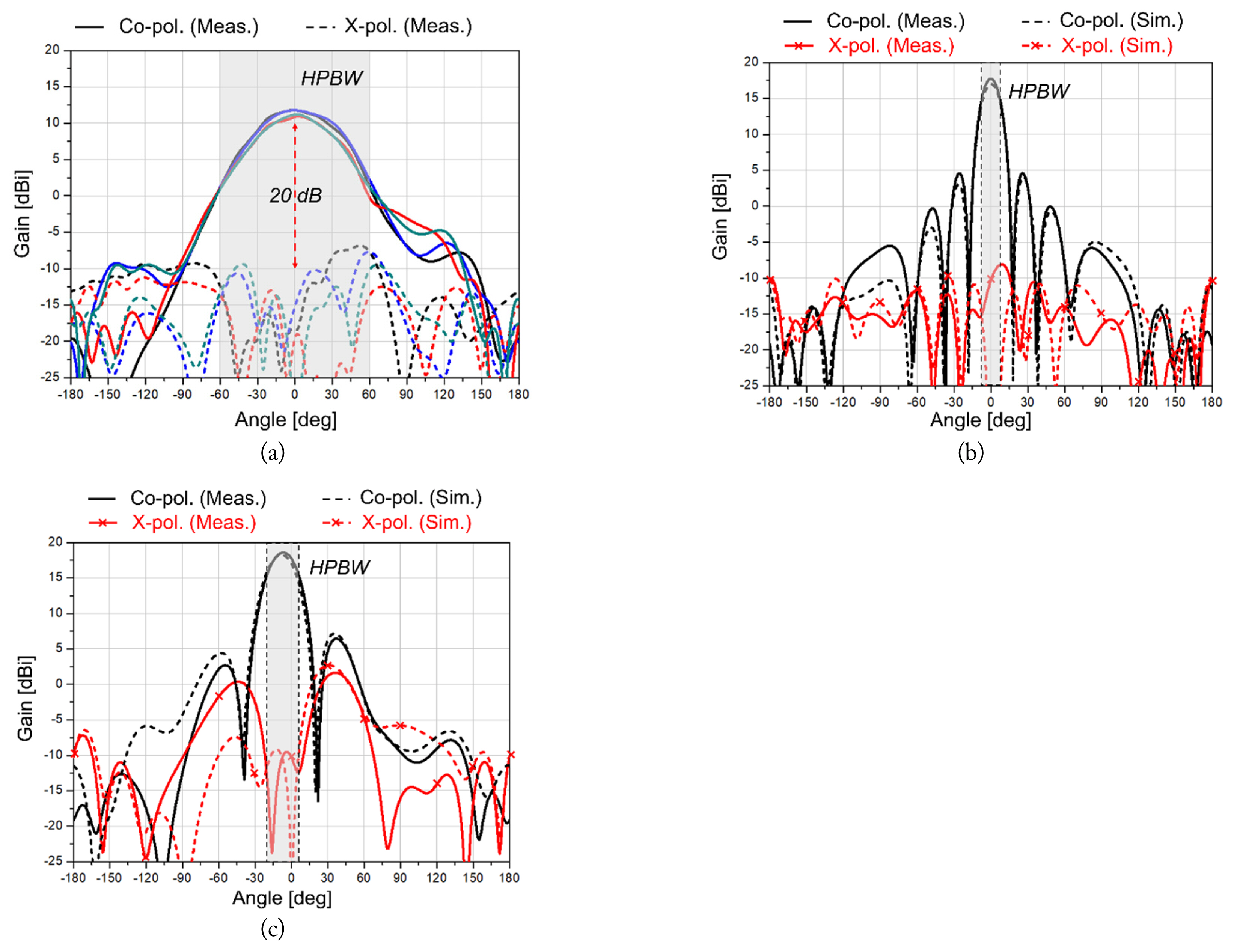
The radiation patterns at 2.11 GHz are plotted in Fig. 8. The azimuth patterns of the subarray column beams, measured at all ports, are shown in Fig. 8(a). The desired HPBW of approximately 65┬░ was achieved by adjusting the beam width using metal walls. The XPD requirements of 20 dB at 0┬░, 15 dB at 30┬░, and 10 dB at 60┬░ were also satisfied. Fig. 8(b) and 8(c) present the azimuth beam patterns and elevation beam patterns of the 3 ├Ś 4 antenna array, respectively. The simulated and measured radiation patterns exhibit good agreement, indicating well-matched results. Moreover, the antenna array exhibits consistently low XPD (< 25 dB) at both ports.
V. PIM Measurement
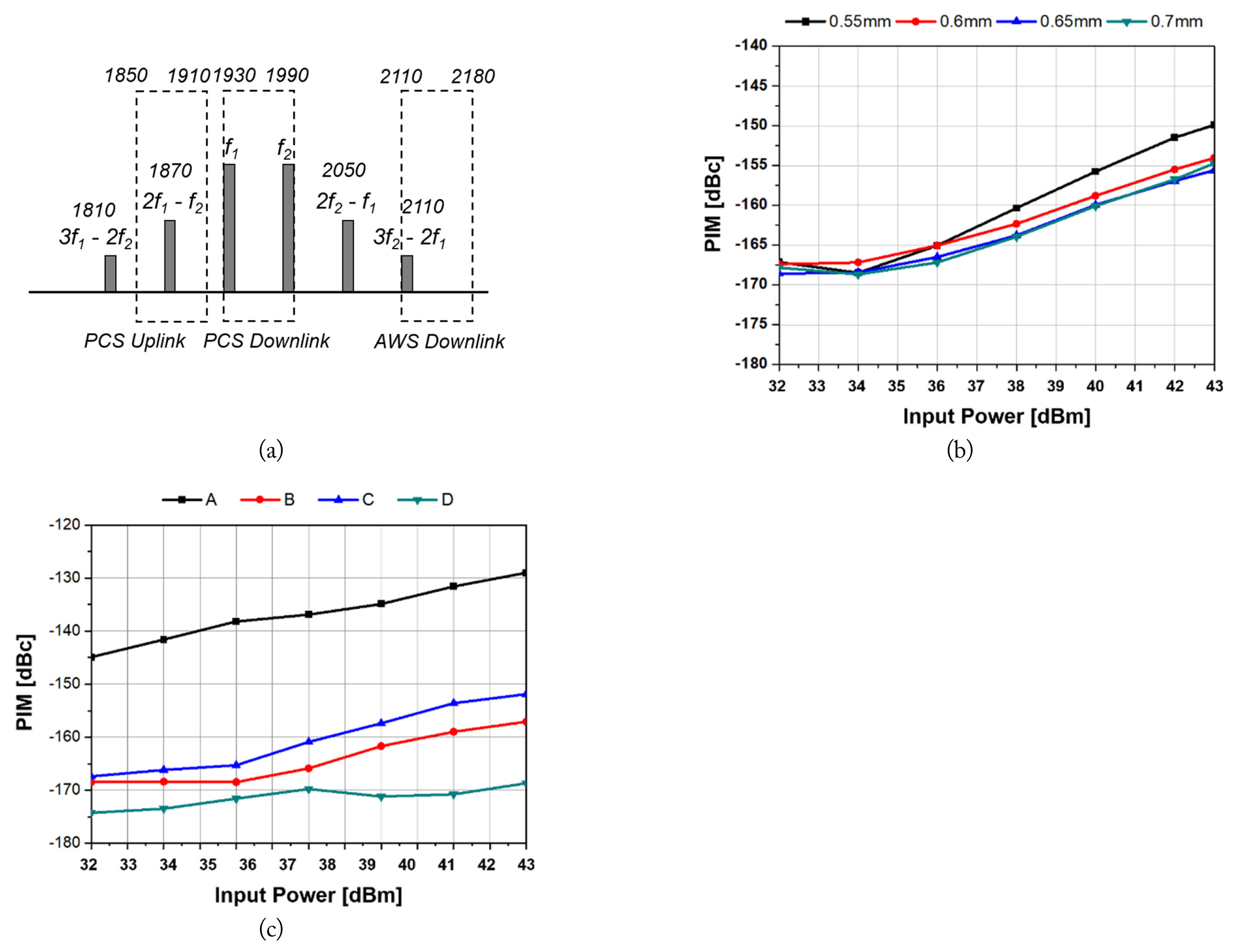
Fig. 9(a) notes the PIM results obtained on mixing two closely located transmitted (Tx) signals. Third-order intermodulation products (IM3) situated close to Tx signals often exhibit relatively higher magnitudes. Therefore, the IM3 of the PCS downlink may fall in the PCS uplink band or the AWS downlink, leading to harmful interferences. PIM is caused by nonlinear junctions, such as loose metal connections and rough metal surfaces, which act as diodes [15]. This is because rough metal-to-metal contacts can cause current crowding, thus generating PIM. Several other factors also contribute to PIM, including the type of substrate material used, quality of the plated-through holes, cleanliness of the PCB, presence of materials with ferromagnetic properties, assembly issues, and even the roughness of a copper conductor.
The PIM levels were measured at each port using the reverse mode of a PIM analyzer. As shown in Fig. 9(b), PIM levels increase with higher input power. The widths of the quarter wavelength lines also show changes, with the narrower line indicating higher PIM levels, since a narrower microstrip transmission line results in a higher power density. Fig. 9(c) illustrates the PIM levels in various scenarios, also presented in Table 1. It is evident that PIM levels are higher when using a thinner PCB since the power density in such a case is also higher. For instance, nickel alloy copper treatment has deleterious effects on PIM performance because nickel is a ferromagnetic material. Stainless steel also comprises ferromagnetic components, as a result of which a decline in PIM may be observed when it is used. Notably, although the materials examined deteriorated PIM performance, PIM was lower than ŌłÆ150 dBc in the case of PCBs with a thickness of 0.8 mm.
VI. Comparison with Previous Studies
Table 2 shows the comparative results of the various previously studied base station antennas [7, 16ŌĆō18]. A comparison of the frequency, number of subarrays, antenna type, fractional bandwidth, fractional port isolation bandwidth, max gain of the subarray, XPD, and front-to-back ratio (FBR) was conducted. The results show a relatively wide bandwidth between the patch antennas, despite the number of subarrays. Furthermore, the proposed design exhibits a relatively better FBR and isolation.
VII. CONCLUSION
A 1:3 power divider featuring a wideband 180┬░ phase shifter, which enables consistent out-of-phase excitations that reduce probe leakage radiation, is proposed in this paper. This power divider was utilized to design a dual-polarized quadruple ╬Ā-probe feed stacked patch antenna array, which achieved a wide bandwidth, high XPD, and high isolation. Furthermore, the proposed structure was verified by employing a 3 ├Ś 4 array. The measurement results indicate that the proposed design works favorably in terms of XPD and isolation while also maintaining sufficient bandwidth and beam performance and exhibiting good PIM performance.