I. INTRODUCTION
The 5G wireless communication is being considered a promising candidate for next-generation cellular systems owing to growing traffic explosion in the existing 4G spectrum and the demand for high data rates. In the next few years, more base stations supporting frequency spectra above and below 6 GHz are expected to be built in multiple countries to enable seamless coverage of 5G services. In this context, high-performance base stations characterized by high yield and low cost must be mass produced to ensure a successful network equipment business. Furthermore, compared to the conventional microwave frequency band, the performance and costs involved in the mmWave spectrum are more sensitive to the packaging structure of the antenna and the radio-frequency integrated circuit (RFIC). Consequently, the integration of these two components needs to be optimized to improve performance and ensure the feasibility of mass production in terms of cost, reliability, yield, and measurement facilities [1–3].
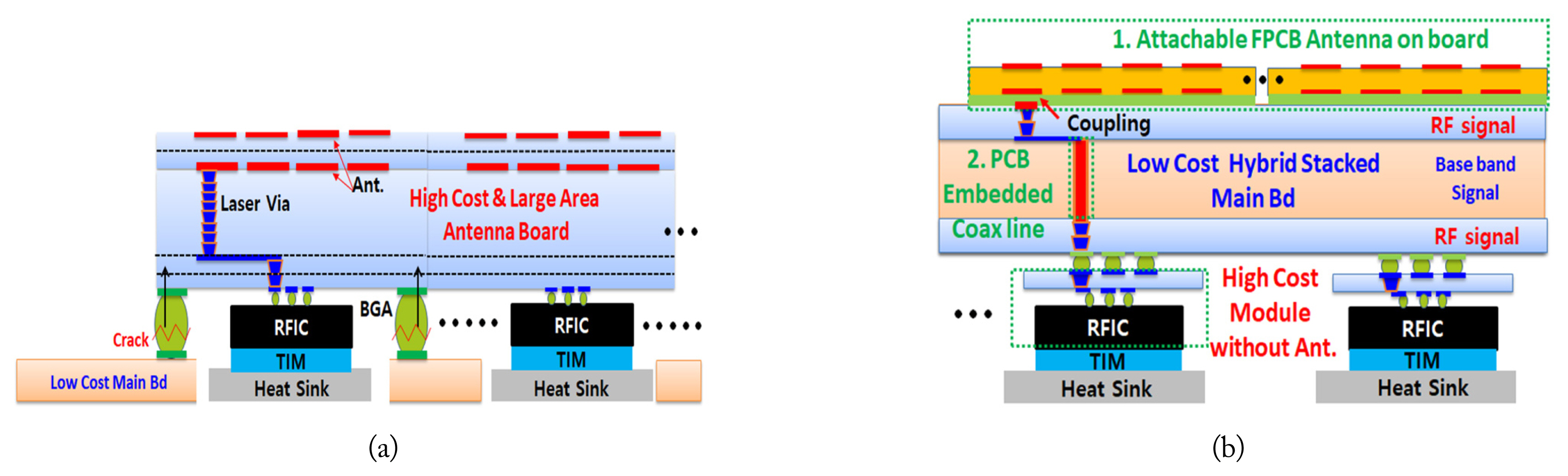
Conventionally, the mmWave antenna-in-package (AiP) module has been implemented in expensive high-end printed circuit boards (PCBs) characterized by low-loss substrates and a high-precision PCB fabrication process to sustain stable performance in the mmWave band. However, the manufacturing cost of such multilayer large-scale PCBs for base stations increases exponentially with an increase in the number of PCB lamination processes using all-stacked aligned laser vias [4–6]. Therefore, most major companies providing mmWave modules integrated with RFIC chips have utilized a module based on AiP for relatively small products, such as mobile devices, despite its high cost.
In this paper, a novel low-cost hybrid PCB structure with an externally attached antenna is proposed. In addition, two innovative solutions are suggested for 39 GHz band application to address antenna performance degradation and vertical RF transition loss in the proposed low-cost hybrid PCB based on a high-loss FR4 substrate: 1) a PCB-embedded coaxial line for low-loss and wide-bandwidth vertical transitions and 2) an external flexible PCB (FPCB) antenna attached to the PCB using adhesive film, leaving a constant gap for coupling.
II. ATTACHABLE FPCB ANTENNA ON HYBRID PCB
Fig. 1(a) illustrates a conventional AiP structure in which the antenna and RFIC chip are integrated into a package composed of a high-end multilayer PCB with a precise all-stacked aligned laser via and low-loss high-end substrates to minimize transition loss from the antenna to the RFIC chip [4, 5]. To fabricate a large AiP structure, the base station requires a large-scale array. This, however, increases difficulties pertaining to mass production in terms of the cost and reliability associated with large high-end PCBs. In addition, to effectively transfer heat from an RFIC chip to air, the RFIC and heat sink must be directly integrated by utilizing a thermal interface material (TIM), as shown in Fig. 1(a). In this context, since mechanical force needs to be applied to maintain stable contact between the TIM and the heat sink, the induced force from the heat sink is transferred to the solder balls situated between the main board and the AiP package. However, this causes reliability issues, such as the appearance of unwanted cracks in the ball over time. The performance of an RFIC chip in an AiP is usually verified with regard to the packaging condition. Therefore, the performance of the AiP integrated with the RFIC and the antenna can be verified by perfuming an over-the-air (OTA) test in a specially equipped chamber composed of a shielding room, absorbers, and horn antennas. In contrast, the proposed package without an antenna can be tested by conducting direct probing on automatic test equipment (ATE). Therefore, a comparison of the test setup conditions indicates that the proposed package can be a promising candidate from the perspective of commercialization and productivity in terms of installation of the complex measurement facilities and processes.
A large-scale main PCB structure that is suitable for the large-scale array antennas used in commercial base stations must support various types of signals, including RF signal lines near 39 GHz and relatively low-frequency signals, such as control, power, and base band signals. Therefore, the conventional AiP structure can be used to recover the high loss of the RF feed line and antenna in the mmWave frequency band by employing high-end PCB substrates and implementing expensive and precise PCB processes, such as all-stacked laser vias. Therefore, the AiPs supporting RF signals are assembled on an FR4 based main board, which supports other low-frequency signals through a ball grid array (BGA).
Compared to the conventional AiP on the main board, the proposed PCB on antenna packaging can be applied to different types of main boards supporting both RF signals and low frequency signals, such as baseband, power, and control signals.
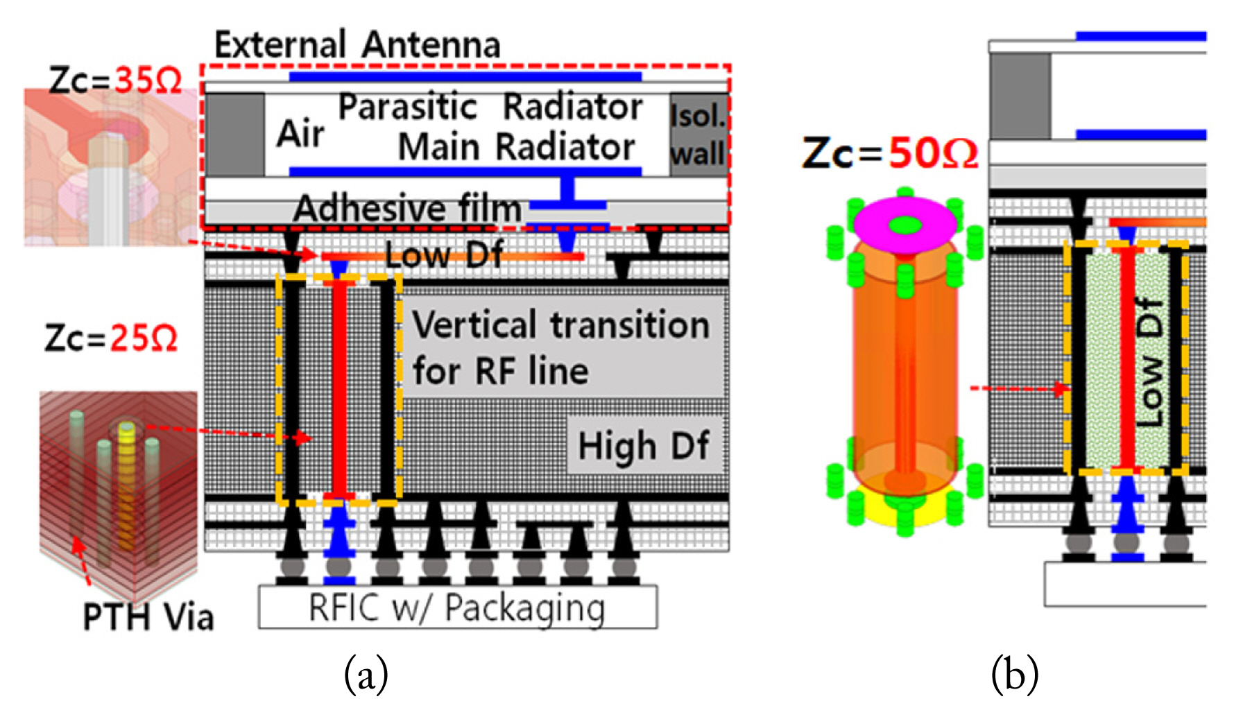
As shown in Fig. 1(b), the main board applied to the hybrid PCB structure, composed of limited top and bottom layers, is attached to a low-loss, high-end substrate and to a precise process for the RF line and the antenna. The other layers at the center of the PCB are composed of an FR4-based low-cost substrate for low-frequency signals. Therefore, the hybrid PCB uses high-end substrates placed symmetrically on the top and at the bottom to minimize mechanical bending, which may occur when using substrates with different thermal expansion rates. The reduction in the number of layers of the high-end PCB substrate at the top and bottom is essential for cost reduction and mass production. However, to achieve a sufficient gap between the antenna and the ground to ensure good antenna performance in the conventional AiP structure, at least 8 layers need to be laminated through an expensive all-stacked laser vias process, which would increase the cost of the embedded antenna for large-scale PCBs exponentially. Therefore, this study added a low-cost novel antenna-assembled structure to the large-scale hybrid PCB. Therefore, the limited 2–3 layers of the high-end substrate and process are only applied to the RF feed line. The array antenna, which requires many layers to yield antenna performance, is externally attached to the board through a coupling-type feed structure using an adhesive film with a constant gap, as shown in Fig. 1(b). The structure of the main radiator situated above the main PCB, composed of a 16 × 16 array (256 antenna elements) and supporting two polarizations per antenna element, was fabricated on a FPCB, as shown in Fig. 2(a). The FPCB, including the main radiator and the coupling pad for coupling to the main board, is attached to the board with an adhesive film of thickness 50 μm, as shown in Fig. 2(b). Precise alignment between the FPCB and the main board was established using a vision camera and align marks. The main radiator can be operated using strong coupling feeding from the coupling pads located between the FPCB and the main board. As shown in Fig. 2(c), additional parasitic patch antennas are assembled on the main board attached to the FPCB antenna to improve antenna efficiency and impedance bandwidth by air coupling. The parasitic antenna, also patterned on the additional FPCB, is assembled on the main board using a metal-based isolation wall to sustain a constant air gap between the main and parasitic radiators, thus providing better isolation between the antenna elements. Therefore, the efficiency and bandwidth of the antenna are improved primarily by adding an air-coupled parasitic radiator.
III. NOVEL PCB-EMBEDDED COAXIAL LINE FOR HYBRID PCB WITH LOW LOSS AND WIDEBAND PERFORMANCE
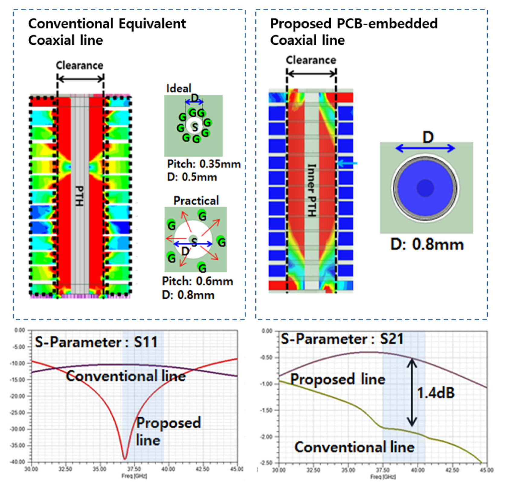
As shown in Fig. 3(a), high-end PCB material can only be applied to the limited top and bottom layers of the hybrid PCB, which pertain to the RF transition line and antenna, for cost reduction. Other low-cost FR4 substrate layers placed at the center of the PCB accounted for the relatively low-frequency signal lines, such as the baseband, power, and control lines. During the PCB assembly process, the FR4 layers were simultaneously bonded through a single lamination process using a low-cost plated through-hole (PTH) via, which was simply perforated through one laminated FR4 layer. Compared to the elaborate laser via process for the all-stacked high-end PCB, the PTH via cannot easily make small holes with dense pitches among the vias during the PCB fabrication process. The conventional vertical transition in the PCB equivalent to the RF coaxial line comprises a single PTH via surrounded by multiple grounded PTH vias. Even the outer wall of the coaxial line is equivalently made of only 3–8 PTH vias. When the operating frequency increases above 30 GHz, the vias equivalent to the outer wall of the coaxial line need to be more densely arranged, with a pitch below 0.35 mm, to achieve a characteristic impedance of 50 Ω and ensure low loss leakage. However, the recommended fabrication specification of the PTH via for mass production allows a pitch of 0.6 mm and a clearance diameter of 0.8 mm. Therefore, the conventional equivalent coaxial line using PTH vias suffers from the inevitable limitation of impedance mismatch and leakage power among sparsely placed and grounded PTH vias. As a result, the characteristic impedance of the equivalent coaxial line is 25 Ω and that of the transition pad located near the transition between the vertical and horizontal lines is 35 Ω. To avoid impedance mismatch, the RF line should be longer so as to adjust the impedance matching. However, the method for impedance matching leads to a narrow impedance bandwidth and additional unwanted feed loss.
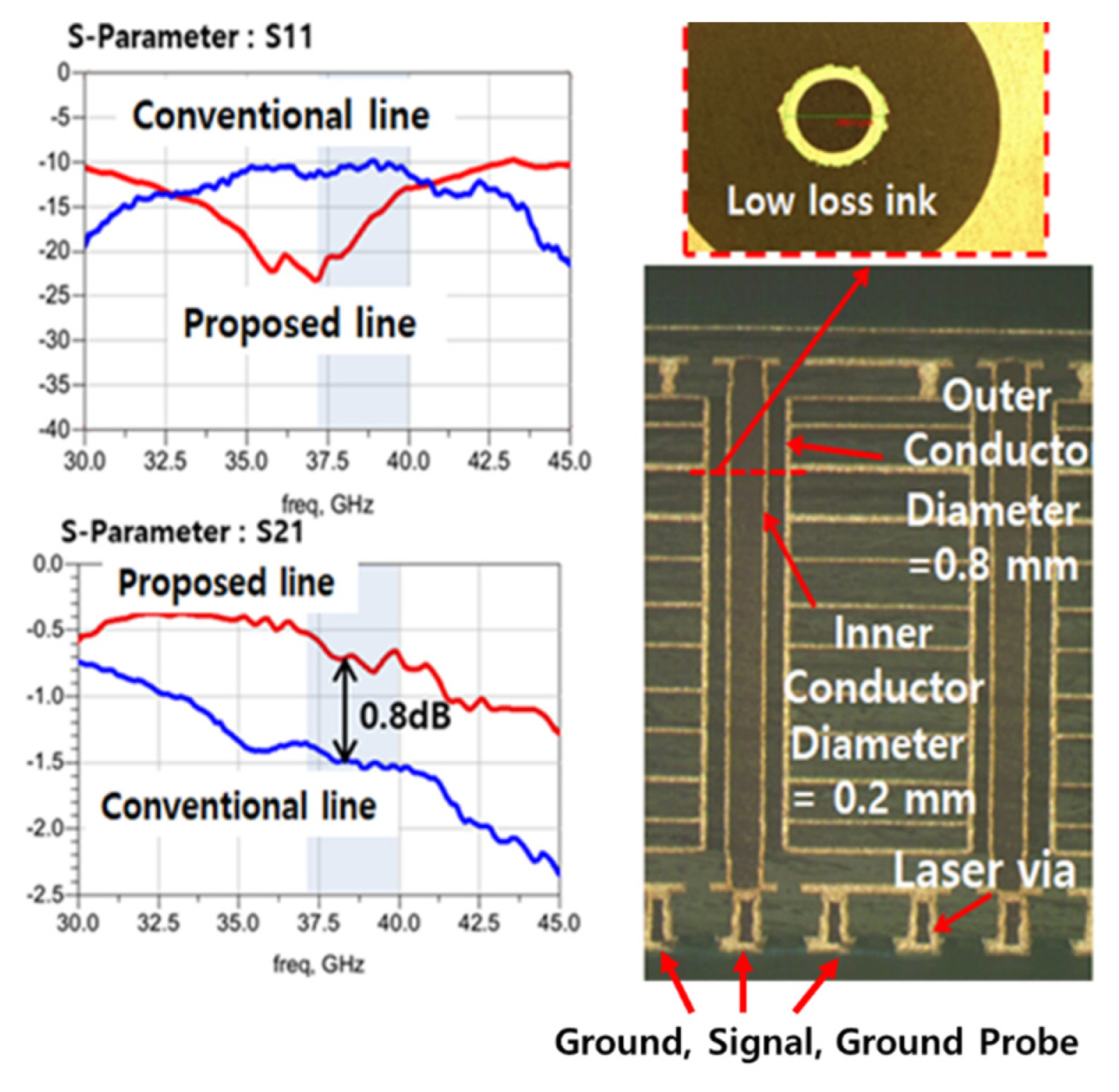
As shown in Fig. 3(b), the novel PCB-embedded coaxial line is an excellent candidate for improving the RF loss in the vertical transition caused by impedance mismatch and the additional loss above 30 GHz caused by limitations in the PCB fabrication specifications. The coaxial line filled with low-loss dielectric material is embedded into the PCB in the 5 mm vertical direction through the high-loss FR4 substrate by conducting additional processes in the PCB fabrication. The coaxial line comprises an outer wall with a diameter of 0.8 mm and an inner signal line with a diameter of 0.2 mm that is fully filled with low-loss ink (εr = 3.5, Df = 0.001 at 10 GHz), similar to the low-loss substrate.
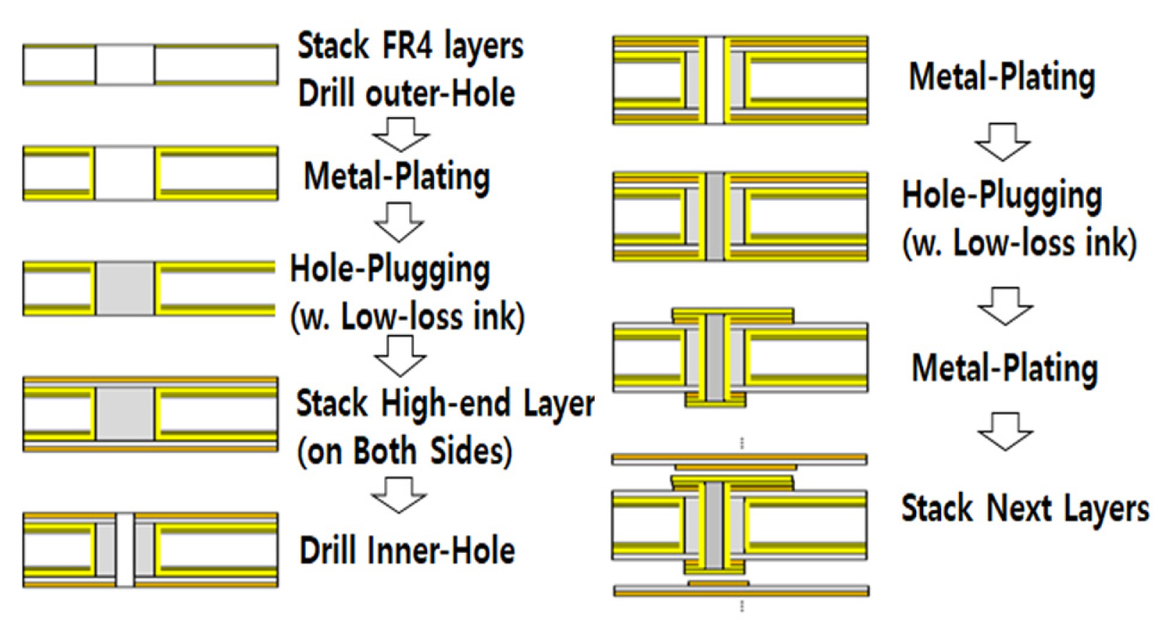
The proposed vertical transition was fabricated within the hybrid PCB, as shown in Fig. 4. First, the centers of the PCB layers based on FR4 were simultaneously bonded using a single lamination process. Next, drilling, metal-plating, and hole-plugging using low-loss ink were performed to fabricate the outer ground wall. For the inner signal line of the coaxial line, the high-end layer was stacked on both sides. Finally, the process was completed by repeated drilling, metal-plating, and hole-plugging.
Fig. 5 presents two simulation results related to impedance matching (S11) and insertion loss (S21) for the vertical transition of the conventional equivalent coaxial line with PTH vias and the proposed PCB-embedded coaxial line. Compared to the conventional equivalent coaxial line with the practically fabricated PTH vias on the hybrid PCB, the proposed coaxial line exhibits enhanced impedance matching over a wider frequency range and an improved insertion loss of approximately 1.4 dB. As shown in the top image of Fig. 5, the field distributions of the vertical transition line, as presented by the electromagnetic field simulation, explain the reason for the proposed coaxial line exhibiting no leakage and producing better insertion loss, while some EM field leaks through the gap between the sparsely surrounded PTH vias.
Fig. 6 (left) shows the measured results of impedance matching (S11) and insertion loss (S21) for the two vertical transitions at approximately 30–40 GHz. While the simulated S21 was 0.5 dB at 39 GHz, the measured value was 0.7 dB. These results are in good agreement with the simulation results. In addition, the fabrication process for the hybrid PCB was verified by examining the cross-sectional view of the proposed coaxial line, as shown in Fig. 6 (right). From the measured results and the cross-sectional view of the PCB, it can be concluded that the proposed coaxial line is a good replacement for the conventional coaxial line in a hybrid PCB, as it exhibits improvements in insertion loss as well as in the bandwidth of impedance matching within the practical fabrication specifications of the PCB. The performance and differences between the conventional PCB embedded coaxial line and the proposed coaxial line are presented in Table 1.
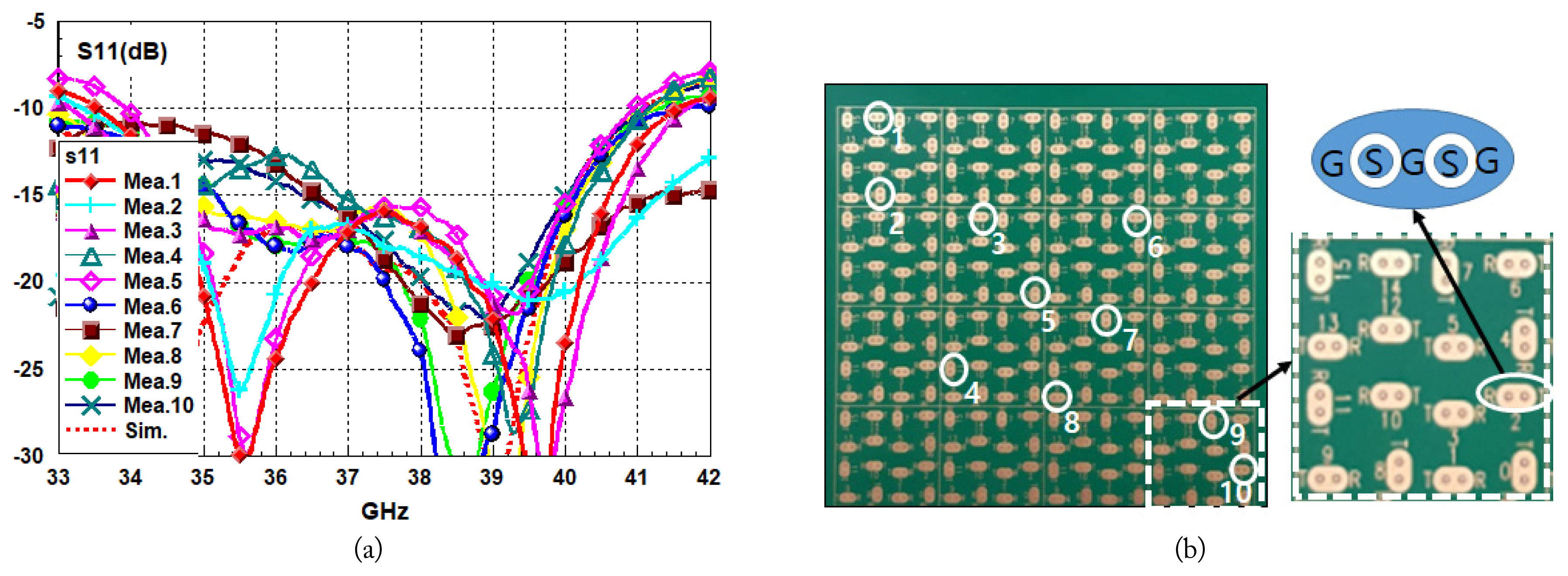
Fig. 7(a) shows the simulation and measurement results pertaining to the antenna impedance (S11) of the main and parasitic antennas assembled on the board using the proposed PCB-embedded coaxial line. To measure the mmWave antenna, the PCB had to be specially designed with a ground-signal-ground (GSG) pad to ensure stable contact with GSG probing without degradation of antenna impedance due to the contact [7]. The results of the measured impedance show a wide bandwidth of 18.6%, approximately 7 GHz, ranging from 34 GHz to 41 GHz, even when using a low-cost PCB fabrication process. Moreover, these estimates are in agreement with the simulation results. In addition, the antenna impedance of the proposed structure can be fabricated and produced within fabrication errors by checking and verifying the variations in antenna impedance at multiple ports placed at various positions in the large-scale PCB, as shown in Fig. 7(b).
A comparison of the performance of the proposed method and that of other similar methods implemented in PCBs with a coaxial line is presented in Table 2. Notably, Boone et al. [8] designed a CPW-coaxial line transition using an etching technique, which presented insertion loss on incorporating CPW lines. Furthermore, Aoyagi et al. [9] implemented a coaxial line by conducting PCB side plating, although it was created in the horizontal direction. Compared to these studies, the proposed method achieved a relatively better insertion loss. Furthermore, the proposed structure offers the advantage of being cost effective, as it does not require implementing significant changes to the existing PCB process.
IV. PERFORMANCE FOR BASE STATION
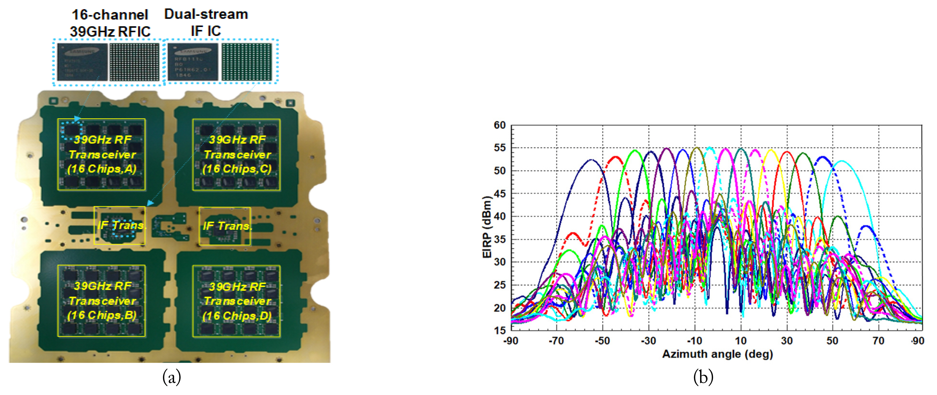
The proposed antenna packaging and external air-coupled antennas, assembled and connected with a 39 GHz CMOS-based 16-channel phased-array transceiver IC [10], as shown in Fig. 8(a), carry out beam-forming functions. The transceiver IC utilizes 4 phase shift bits, thus allowing for adjustment of the phase values applied to each antenna, with the unit of adjustment being 22.5°. Sixteen RFIC chips were assembled on the antenna-assembled board to support the 256 (16 × 16) element antenna per stream. Finally, set-level beam-forming results were obtained.
To achieve beamforming, a progressive phase (α) was applied to an array antenna with half-wavelength spacing. The main beam direction (θ) of the antenna was calculated using the following formula [11]:
When the progressive phase was applied to the 22.5° to 157.5° range, the main beam direction of the antenna ranged from 7.2° to 61°. The experimental results pertaining to the radiation pattern when applying the progressive phase to each antenna in multiples of 22.5° are presented in Fig. 8(b). The base station exhibits a wide scanning range of over 120°, ranging from −60° to 60°, at 39 GHz. At boresight, it exhibits an effective isotropic radiated power (EIRP) of 55 dBm per stream. Notably, the expected peak gain from the measured EIRP and conduction power was 29 dBi, with a 3 dB beamwidth of approximately 6° at 39 GHz. The efficiency was almost above 95% without considering feed network loss. Therefore, the measured results of the beam-forming performance, which include the performance of the system, such as antennas, IC transceivers, and other related functions, satisfy the beamforming performance of commercial base stations.
V. CONCLUSION
This study investigated a novel packaging and antenna-assembled large-scale board for 39 GHz commercial base stations. In addition, two innovative solutions—an externally attachable flexible PCB antenna and a PCB-embedded coaxial line—were verified to satisfy the required antenna impedance and beam-forming performance. By splitting the antenna from the packaging and board and subsequently applying the two proposed solutions, improved productivity was achieved by the large-scale array for the base station in terms of cost and reliability without sacrificing performance.
Furthermore, this study verified the beam-forming measurements of 256 dual-polarized antenna elements using a 39 GHz CMOS 16-channel transceiver IC, exhibiting an EIRP of 55 dBm at boresight and a steering range of >±60°.
Therefore, the combination of the proposed structures and solutions is a good candidate for use in commercial base stations with large-scale arrays operating at 39 GHz or beyond.