500 MS/s 4-Bit Flash ADC with Complementary Architecture
Article information
Abstract
This paper proposes a 500 MS/s 4-bit flash analog-to-digital converter (ADC) featuring a differential input voltage range of 1.2 Vpp operating at a supply voltage of 1.2 V. Although the proposed circuit utilizes a conventional flash ADC structure, its track and hold circuit, driving buffer, and preamp circuits corresponding to the analog stages are designed using complementary architecture to attain a sufficient swing range even at a low supply voltage. Notably, the proposed structure satisfies the error requirements. The error source of the flash ADC, such as the comparator’s input referred offset, did not degrade its performance, while the use of a calibration circuit, characterized by power consumption and area burdens and increased complexity, could also be avoided. Therefore, the proposed flash ADC met the error requirements, such as the comparator’s input referred offset, without the need for calibration circuits. The chip, fabricated using the TSMC 65 nm process, covers an area of 1,160 × 950 μm2 and consumes 78 mW of power. Furthermore, its signal-to-noise and distortion ratio and spurious-free dynamic range were measured to be 23.36 dB and 30.26 dB, respectively, at a sampling frequency of 500 MHz.
I. INTRODUCTION
Flash analog-to-digital converters (ADCs) exhibit faster performance than other types of ADCs, as they can simultaneously compare an analog input voltage with multiple reference voltages using comparators. This makes them suitable for applications that require high-speed operation, such as high-speed links, ultra-wideband receivers, and video processors [1–5]. Furthermore, they exhibit low conversion latency and, considering the operating speed of the digital circuit in the legacy process, have several advantages over successive approximation register (SAR) ADC.
However, the resolution of flash ADCs is limited by offset issues caused by comparators. Furthermore, with supply voltage decreases and process technology becoming more advanced, the swing range of signals in analog circuits has continued to decrease, making it increasingly important to design comparators that minimize the offset in flash ADCs.
In [6], the offset was calibrated by current trimming using a current digital-to-analog converter (DAC). However, since a current DAC was required for each comparator, the total power consumption increased. Furthermore, [7] calibrated the offset by adjusting the bulk bias of the PMOS constituting the comparator, thus consuming relatively little power. However, the area of the digital logic circuit for calibration occupied a significant portion of the chip. Meanwhile, instead of calibrating the input referred offset of the comparator, [8] proposed a method for designing a flash ADC considering the full scale of the 2σ value of the offset using the stochastic distribution as the reference level. This method offered the advantage of addressing issues related to power consumption and the area of the calibration circuit. However, the full scale was too small to be vulnerable to the influence of noise, thus intensifying the problem as the supply voltage decreased.
Recently, a method for converting the difference in the analog input voltage into a difference in time using a voltage-to-time-difference converter was proposed [9]. Unlike previous methods, this method accounts for a relatively wide input voltage range, even for a low supply voltage. However, the mismatch in the R-C delay line, which is to be used in the process of converting the difference of time into digital output, not only limits the gain error and input dynamic range of ADCs, but is also more sensitive to the sampling jitter of the clock than the flash ADC structure of a basic voltage domain.
The flash ADC proposed in this paper adopts a conventional flash ADC structure, but its track and hold circuit, driving buffer, and preamp circuits corresponding to the analog stages are designed using complementary architecture to attain a considerable swing range, even at a low supply voltage. Therefore, it offers the advantage of satisfying requirements while also not degrading the flash ADC performance, coupled with the possibility of avoiding the use of a calibration circuit, which burdens both power consumption and area and increases complexity.
Section II presents the architecture adopted in this research, while Section III describes the circuit. In Section IV, the sources of error, such as noise or offset, are identified and examined, while Section V shows the measurement results. Finally, Section VI concludes this study.
II. ARCHITECTURE
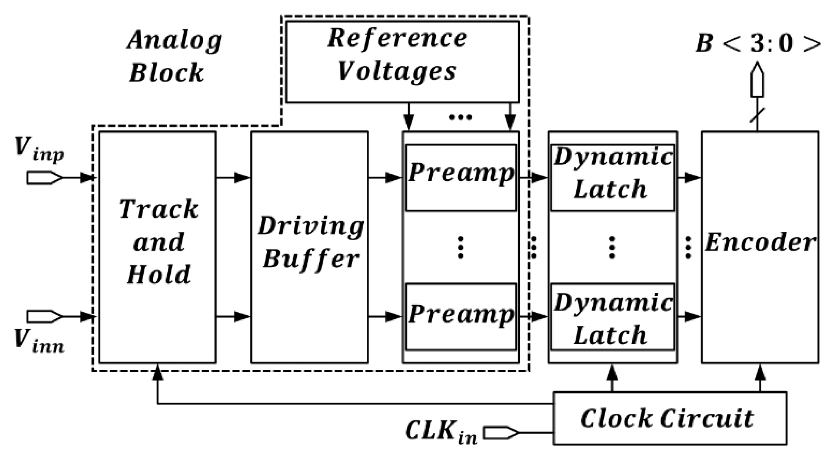
Fig. 1 presents a block diagram of the proposed 4-bit flash ADC, comprising a track and hold, a driving buffer, and a reference voltage generator corresponding to the analog stage. A dynamic latch, encoder, and clock circuits corresponding to the digital stage are also included.
The track and hold samples analog signals, which will be converted into digital signals. A driving buffer is a circuit that is required to drive multiple preamps at high speed. The reference voltage generator generates a reference voltage that is then used to carry out comparisons to determine the level of analog input voltage. Preamps amplify the difference between the analog input signal and the reference voltage in advance so as to prevent the metastability issues that may occur when an extremely small difference in voltage enters the dynamic latch.
The dynamic latch serves to amplify the signal to a digital-level voltage by amplifying the output of the preamp. The outputs of each dynamic latch correspond to the conversion of the analog voltage into a digital thermometer code. Finally, the encoder converts the thermometer code into binary code. Clock circuits are responsible for providing and driving clock signals appropriately.
The track and hold, driving buffer, and preamps corresponding to the analog stage were assigned a complementary design composed of parallel NMOS and PMOS structures to operate against a differential input/output voltage of 1.2 Vpp. Therefore, considering the full-scale range of the input analog voltage and the number of bits as 4, the magnitude of the 1LSB of the designed ADC was expressed as shown in (1):
To ensure that the input referred offset of the comparator stage, consisting of the preamp and dynamic latch, does not degrade the performance of the entire ADC, it should be sufficiently smaller than 0.5 LSB when converted into LSB units. Notably, circuits designed according to a complementary architecture mitigate offset requirements at the comparator stage by increasing the full scale of the ADC. A detailed description of the complementary structural circuits constituting the analog stage is described in Section III.
III. CIRCUIT DESCRIPTION
1. Track and Hold
Fig. 2 depicts the track and hold circuit. Since it should operate in the differential input/output voltage range of 1.2 Vpp, it was implemented as a CMOS switch using both the NMOS switch and the PMOS switch. In addition, to improve the nonlinearity caused by the influence of switch parasitic capacitance, a dummy switch of the same length and half the width was added [10]. This simple structure was adopted considering a low-resolution ADC design target.
Fig. 3 presents the equivalent model of the track and hold circuit in the CK (logic high state) under the condition that the main switch is turned on. Ignoring the dummy switch, the track and hold circuit is modeled by including an equivalent resistor and a load capacitor, in which the resistances of the NMOS and PMOS are parallelly placed. The maximum voltage input to the track and hold circuit was found to be
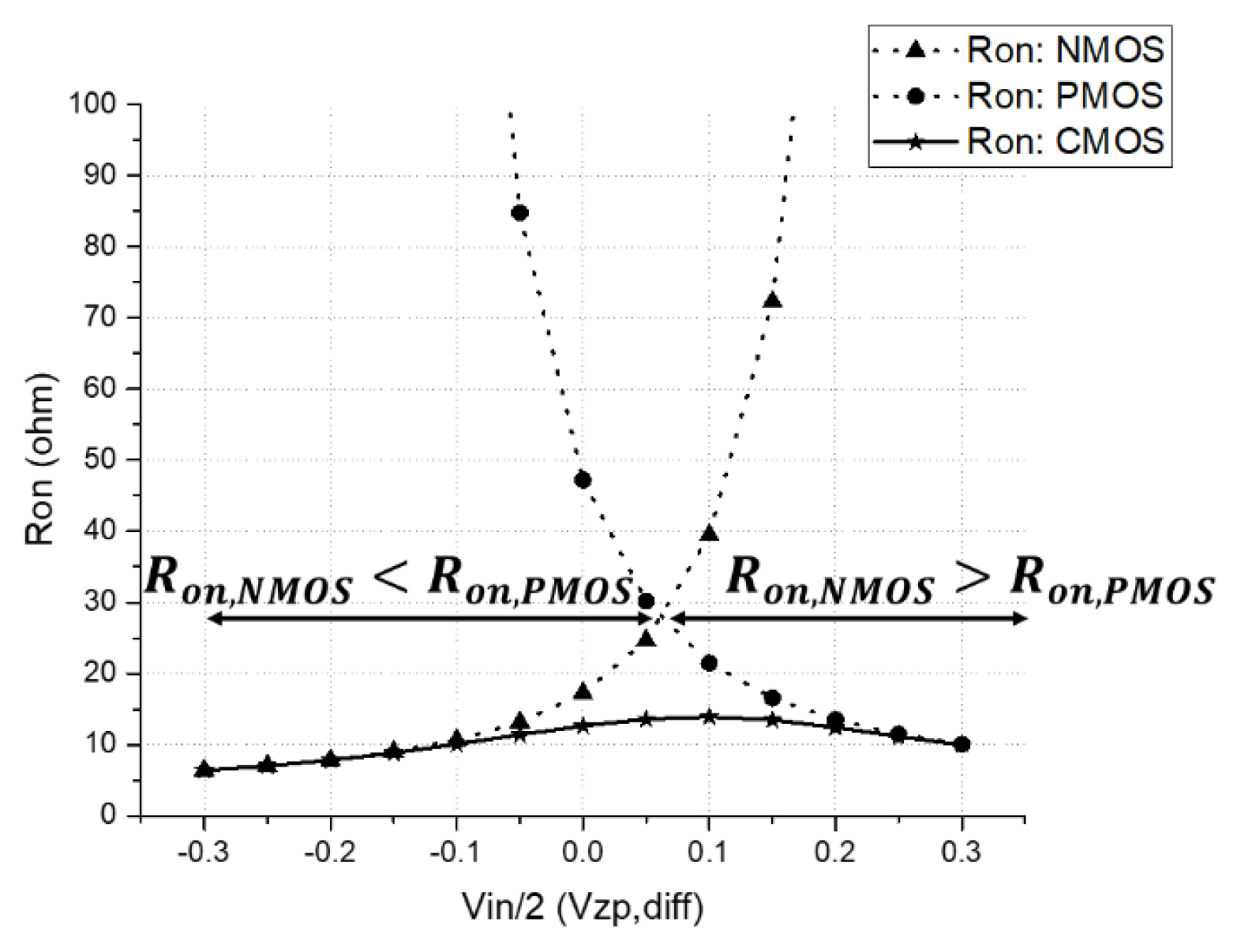
Fig. 4 shows the simulation results of the Ron of each switch used in this design for the considered input voltage range. The Ron of the NMOS is small when the input voltage is small, while that of the PMOS is small when the voltage is large.
This indicates that the Ron of the CMOS bears a low impedance of about 15 Ω or less with respect to the entire input voltage range, with an impedance variation of 10 Ω or less. Therefore, the track and hold was designed to work well with the differential input voltage range of 1.2 Vpp, which represents the full scale of the ADC.
2. Driving Buffer (Source Follower)
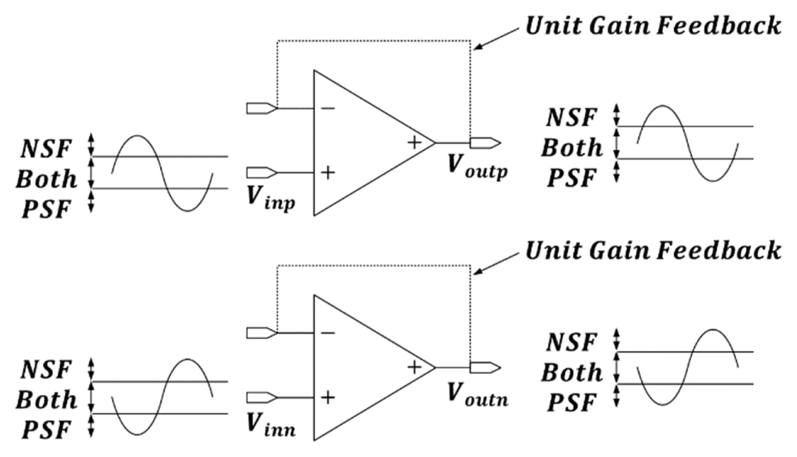
Fig. 5 displays a block diagram of the driving buffer. Since the differential signal must be driven, two buffers were required—each of which was implemented by applying the unit gain feedback to the amplifier of the source follower type. The output impedance of the amplifier was directed at the source of the transistor. To highlight this aspect, this amplifier is referred to as the source follower type in this study. Since the driving buffer must also operate on a sufficient input voltage range corresponding to the full scale of the ADC, the amplifier of each source follower type was designed using complementary architecture.
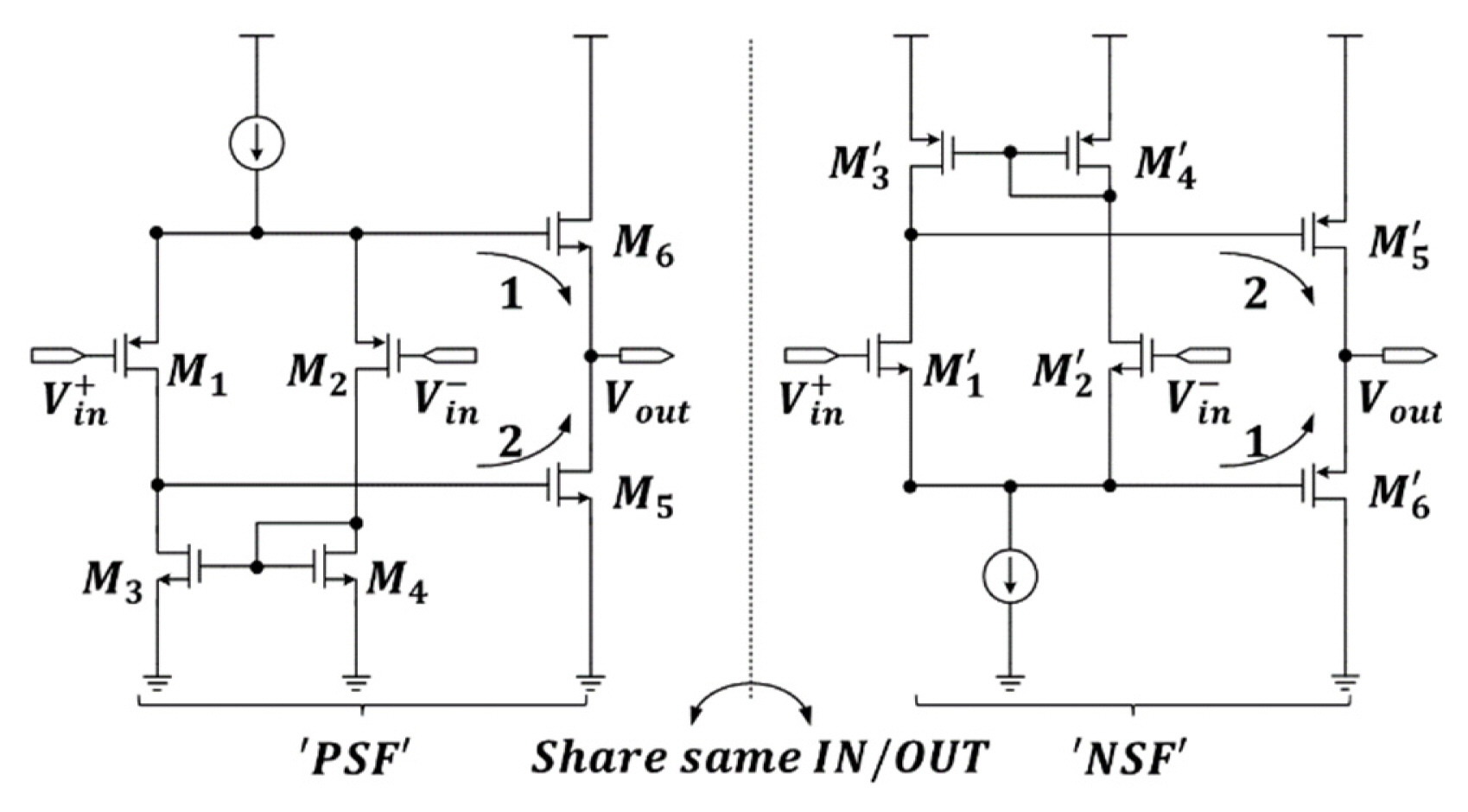
Fig. 6 depicts a circuit of the amplifier of the source follower type used in the driving buffer. The amplifier with a PMOS input stage is termed PSF, while that with an NMOS input stage is termed NSF.
The two amplifiers, expressed as PSF and NSF, operate as one amplifier by sharing the same input and output nodes. In this context, an analysis of the feedforward gain of the amplifier had to be conducted, since the driving buffer operates by applying the unit gain feedback to the amplifier of the source follower type, as shown in Fig. 6. For this purpose, the
First, the Vout node was shorted, with the flowing-out current to the Vout node defined as isc. Then, the transfer gain from input nodes isc to isc was defined as Gm. As shown in Fig. 6, considering the two current paths—1 (source follower path) and 2 (common source path)—the isc can be expressed as (2 ):
Furthermore, Gm,1 and Gm,2 can be expressed using the small signal parameters calculated from (3) and (4):
The output impedance from the Vout node was obtained using (5):
Therefore, the gain from the
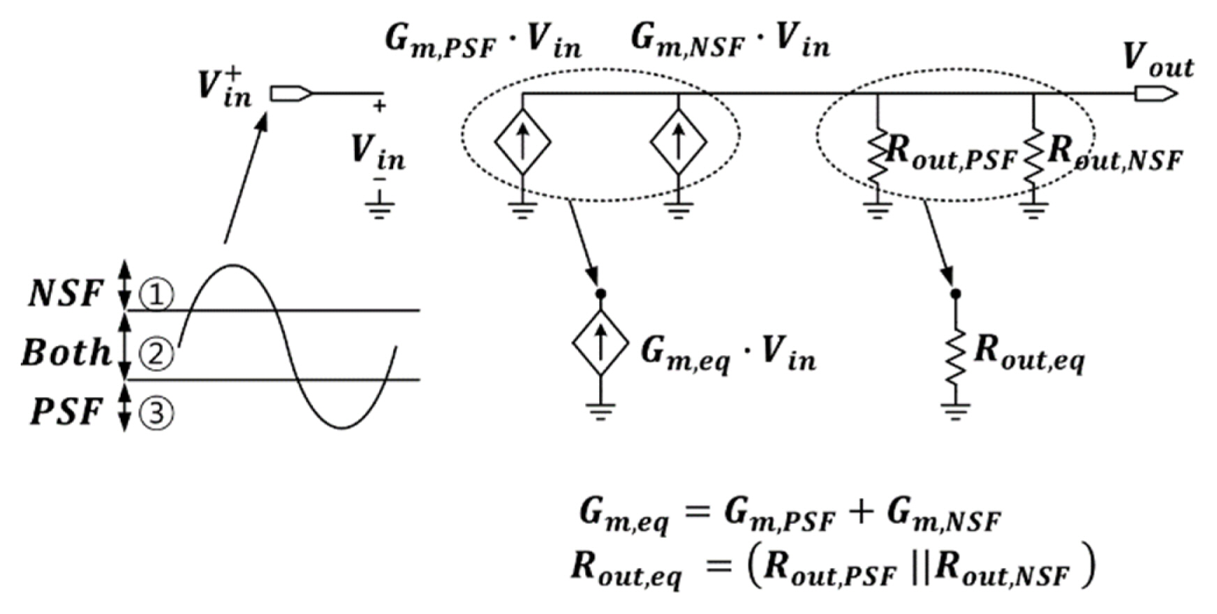
Fig. 7 shows the Norton equivalent model of the source follower type amplifier used for analyzing the effect of the PSF and NSF amplifiers sharing input/output nodes. The equivalent model can be expressed as a dependent current source that generates a current of Gm,eq·Vin and an output resistance of Rout,eq.
For the analysis, the range of the input voltage was considered from 1 to 3, divided according to magnitude. The voltage range corresponding to 1 indicates that the tail current sources of the NSF and PSF are in the saturation and triode regions, respectively. The voltage range corresponding to 2 refers to both tail current sources located in the saturation region. Finally, the voltage range corresponding to 3 refers to when the tail current sources of the PSF and NSF are in the saturation and triode regions, respectively.
The equivalent transconductances Gm,eq were also analyzed according to the magnitude of the input voltage. Drawing on the range of the input voltage expressed by the number 1, the Gm,NSF was expressed as the sum of (3) and (4), since all transistors constituting the NSF were located in the saturation region. However, in the case of the PSF, the tail current source falls in the triode region, which means that most transistors lie in the triode region or the cut-off region because of reduction in the total bias current. Therefore, since the Gm,PSF exhibits negligibly smaller values than the Gm,NSF, the Gm,eq can be approximated to the same size as the Gm,NSF. With respect to the range of the input voltages expressed by the number 3 under the same principle, Gm,eq can be approximated to the same value as Gm,PSF.
In the case of the range of input voltage expressed by the number 2, since the transistors constituting the two types of amplifiers are located in the saturation region, they cannot be approximated by Gm of either type. In other words, it has Gm,eq twice as much as Gm,eq for an input voltage of 1 or 3.
This time, the equivalent output resistances Rout,eq were analyzed according to the magnitude of the input voltage. Drawing on the range of the input voltage expressed by the number 1, the transistors constituting the NSF amplifier all lie in the saturation region, as a result of which the Rout,NSF is expressed using the same value as (5). On the other hand, PSF exhibits negligible values in parallel resistance compared to Rout,NSF due to the effect of reduced total bias current. Since the tail current source falls in the triode region, as described above, Rout,eq can be approximated to the same size as Rout,NSF. With respect to the range of input voltages expressed by the number 3 under the same principle, Rout,eq can be approximated to the same value as Rout,PSF. Meanwhile, in the case of the number 2, since the Rout,eq cannot be approximated by the output resistance of the type, it is expressed as (Rout,PSF||Rout,NSF).
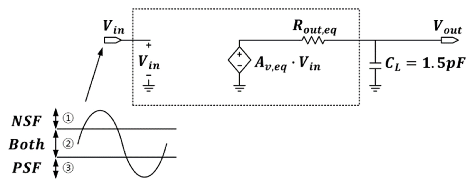
Fig. 8 outlines the Thevenin equivalent model of the driving buffer. The effect of applying unit gain feedback to the equivalent model of the amplifier in Fig. 7. The equivalent model can be expressed as a dependent voltage source that generates a voltage of Av,eq·Vin and an output resistance of Rout,eq. As shown in Fig. 7, equivalent transconductance and output resistance were employed for the input voltage range. Furthermore, drawing on (3)–(5) for the input voltage range represented by numbers 1 and 3, the equivalent voltage gain Av,eq in Fig. 8 can be represented as (7):
Furthermore, for the range of the input voltage expressed by the number 2, Av,eq can be expressed as (8):
Thus, regardless of the input voltage magnitude, the equivalent voltage gain Av,eq in the Thevenin equivalent circuit of the driving buffer is approximated to the same value. Similarly, an equivalent output resistance to the input voltage range was used, as illustrated in Fig. 7. Furthermore, for the input voltage range represented by the numbers 1 and 3, an equivalent output resistance of Rout,eq is considered, as specified in (9):
For the range of the input voltage expressed by the number 2, the Rout,eq was expressed as (10):
This indicates that the magnitude of the output resistance in the Thevenin equivalent circuit of the driving buffer varies according to the input voltage magnitude. Considering that the size of
Fig. 9 presents the DC transfer function of the output voltage with respect to the input voltage of the designed driving buffer. To verify the driving capability, the simulation was performed considering an output impedance of 50 Ω. The driving buffer was designed to drive the load well in the differential input voltage range of 1.2 Vpp, which represents the full scale of an ADC.
3. Preamps
Fig. 10 presents a block diagram of the designed preamp equipped with a complementary operational transduction amplifier (OTA) structure in which the NMOS and PMOS input stages are parallelly located. The stages contribute to amplifying the difference between the differential input signal (Vin) and the differential reference voltage (Vref). Notably, the differential reference voltage is generated from the nodes of each resistor through voltage division by applying the maximum reference voltage
Fig. 10(a) is a block diagram illustrating a case where the positive reference voltage Vrefp is greater than the negative reference voltage Vrefn. It was considered that the NMOS input stage operates well for a voltage higher than Vcm, while the PMOS input stage operates well for a voltage lower than Vcm. Therefore, if the transconductance of the OTAs with the NMOS and PMOS input stages are the same as Gm and the output load resistance is expressed as Rout, the transfer function equation of the input/output in Case 1 can be expressed as (11):
Meanwhile, Fig. 10(b) is a block diagram for a case where the negative reference voltage Vrefn is greater than the positive reference voltage Vrefp. This case adhered to the same considerations made in the previous case. As a result, in the preamplifier depicted in Fig. 10(b), the phases of the input voltage, reference voltage, and output voltage are all inverted compared to the preamplifier in Fig. 10(a). The transfer function equation of input/ output in Case 2 is noted in (11) in the same manner as in Case 1.
Fig. 11 outlines a schematic of the preamplifier. The positive input node of the PMOS input stage is indicated as
Subsequently, the summed current was copied by M5 and M6 and flowed to M7, M’7, M8, and M’8, which acted as active loads to generate an output voltage. Assuming that the transconductances gm1,2 of M1 and M2 and the transconductances gm3,4 of M3 and M4 are the same as gm,eq, the small signal gain achieved by the preamplifier is expressed as (12):
Fig. 12 denotes the preamps within the designed ADC, along with the resistor ladder that generates the reference voltage. Since 15 reference voltages with 4-bit resolutions were required, 15 positive and negative reference voltages were generated in the resistance array. As described in Fig. 10, the preamplifier shown in Fig. 12 was divided based on two cases—the first case pertains to when the positive reference voltage Vrefp is greater than the negative reference voltage Vrefn and the second case considers the positive reference voltage Vrefp to be less than the negative reference voltage Vrefn.
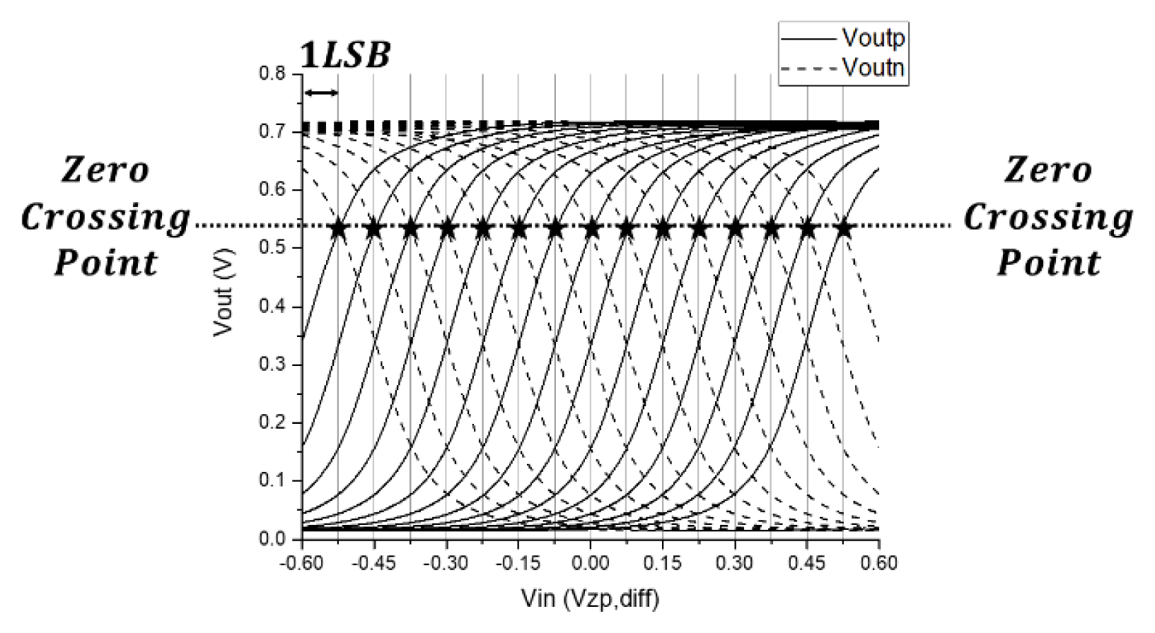
Fig. 13 illustrates the output voltage of each of the 15 preamplifiers when the input differential voltage changes from the smallest to the largest. The results confirm that each preamplifier performs amplification based on a zero-crossing point corresponding to the 15 reference voltages.
IV. ERROR SOURCE CONSIDERATION
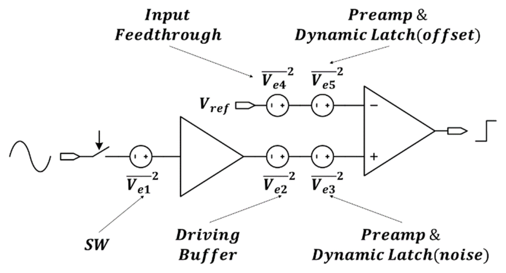
This section examines the error sources that affect the performance of the ADC designed in Fig. 14. Ve1 is an error caused by the kT/C sampling noise modeled on the output node of the sampling switch. Ve2 indicates an error caused by the output referred noise of the driving buffer. Meanwhile, Ve3 is an error resulting from the input referred noise in the preamplifier and dynamic latch, while Ve4 is an error modeled into the reference voltage node due to the input feedthrough. Furthermore, Ve5 refers to an error caused by the input referred offset of the preamplifier and dynamic latch.
On using one/small number of preamplifiers and dynamic latches, such as SAR ADC or pipeline ADC, the offset resulted in static errors in the entire curve and, as a result, cannot be modeled as noise performance. However, in the case of a flash ADC where multiple preamplifiers and dynamic latches are placed parallelly, each offset is different, which appears to be a differential nonlinearity (DNL) performance degradation—a local error for each code—affecting the performance of the entire ADC. Assuming a sufficiently large number of comparators, a model where the distribution of the DNL errors arising from the offset of each comparator forms a uniform pdf, which is later combined with the quantization noise pdf to degrade the signal-to-noise ratio (SNR), is considered. In other words, DNL error can be modeled as a noise model.
Considering the actual circuit as a differential circuit, the effect of each error source is listed in Table 1 as mVrms and LSB units, considering the full scale of the ADC. Furthermore, in the case of the input feedthrough corresponding to Ve4, the low frequency (10 MHz) and high frequency (250 MHz) are separately displayed since input feedthrough depends on the input frequency. The total error considering the influence of each error source was observed to be 0.07 LSB at low frequency and 0.1 LSB at high frequency. Therefore, it can be established that the performance degradation caused by the error source is sufficiently smaller than 0.5 LSB, which is negligible compared to the effect of the quantization error.
V. MEASUREMENT RESULTS
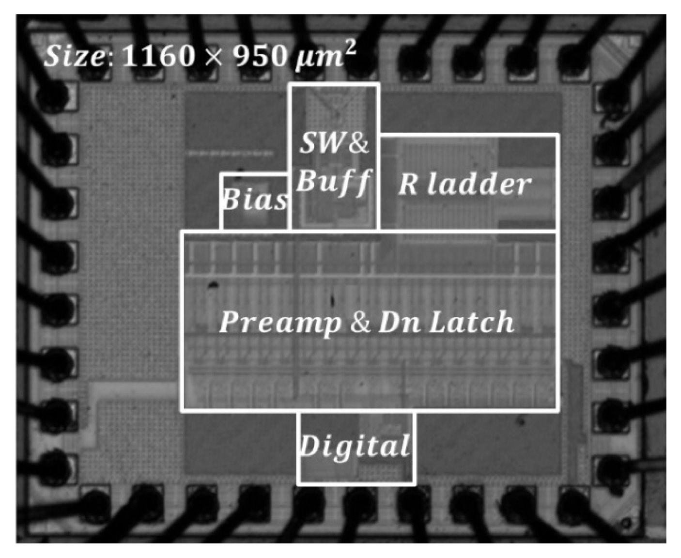
The proposed circuit was implemented using the TSMC 65 nm CMOS process. The chip, pictured in Fig. 15, consists of the proposed flash ADC. The chip area of the proposed ADC is 1,160 × 950 μm2, while its maximum input frequency is 250 MHz and operating sampling frequency is 500 MHz. With a supply voltage of 1.2 V, the ADC’s current consumption is about 65 mA.
Fig. 16(a) shows the measured DNL curve, where a higher DNL is observed for codes 1 and 14 due to the influence of voltage drops resulting from metal parasitic resistance at the resistor-ladder layout. Fig. 16(b) shows the measured integral nonlinearity (INL) curve. For the same reason as the DNL, the INL measurement results consistent with the expected values.
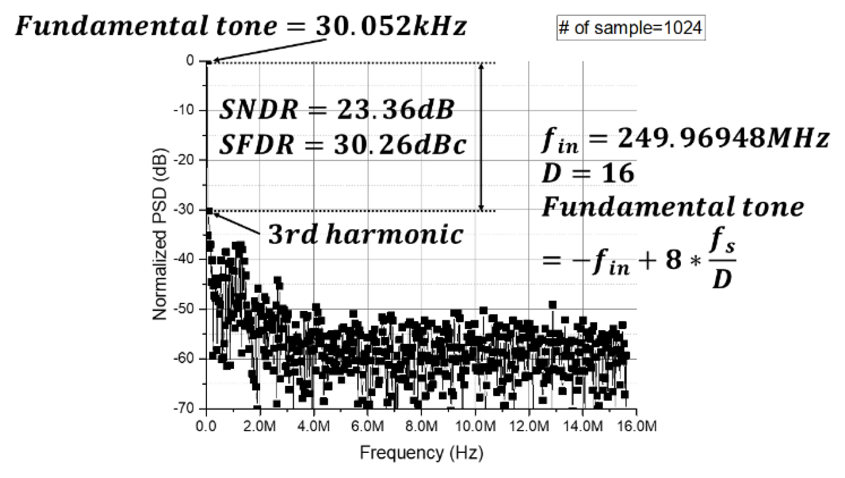
Fig. 17 presents a graph of the fast Fourier transform (FFT) results that the ADC output obtained when 250 MHz—the Nyquist input frequency—was applied at a sampling frequency of 500 MHz. The actual input frequency was applied by accounting for coherence. In addition, the frequency spectrum obtained through the FFT is the result of measurements conducted using a decimator designed on the chip for the measurement of high-speed ADCs. The decimation factor was set to 16. The frequency spectrum in Fig. 17 displays a signal-to-noise and distortion ratio (SNDR) of 23.36 dB and a spurious free dynamic range (SFDR) of 30.26 dB.
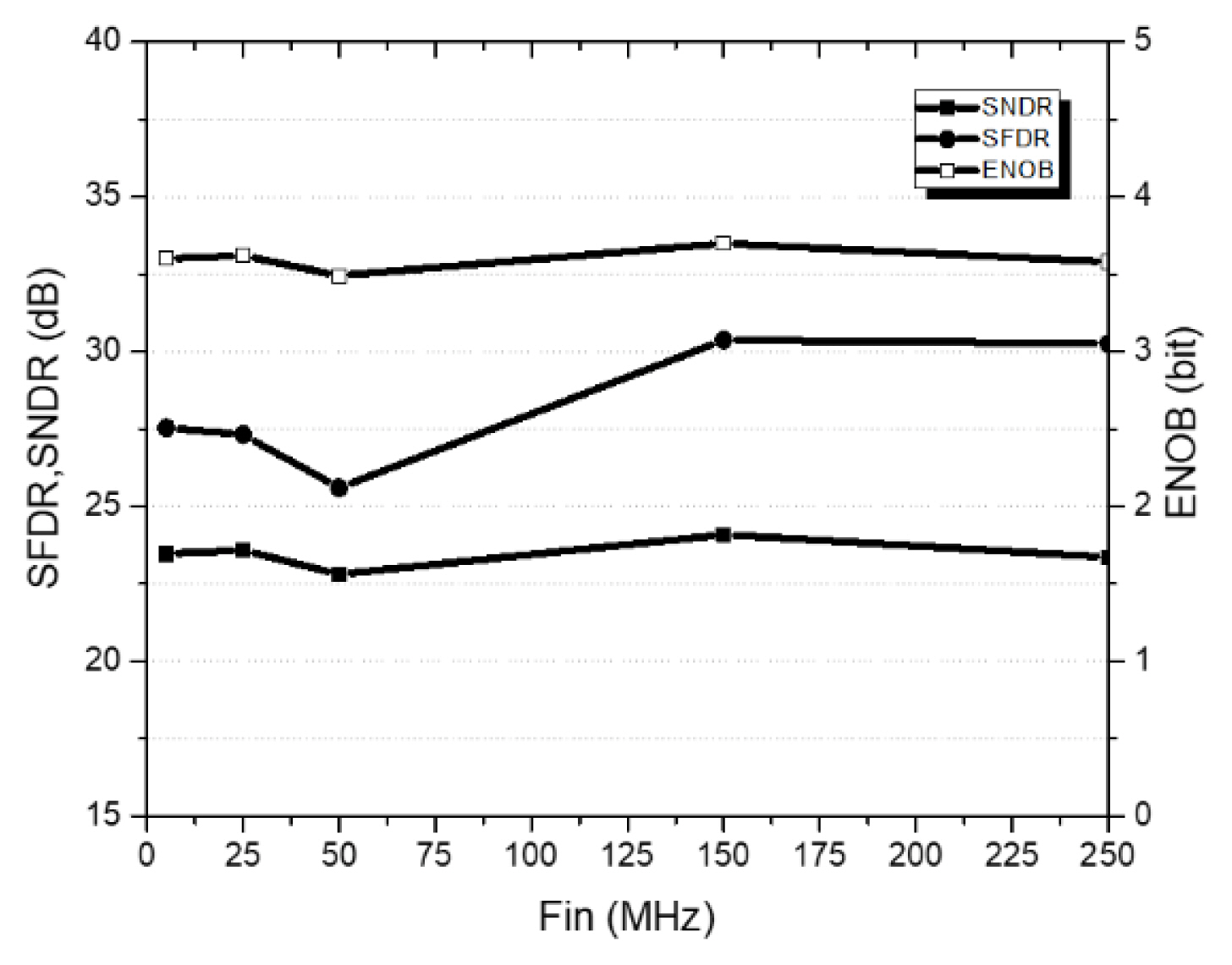
Fig. 18 shows the measurement results of the effective number of bits (ENOB), SFDR, and SNDR for the input frequency at a sampling frequency of 500 MHz. ENOB of 3.6 bits was obtained at a low input frequency (5 MHz), while ENOB of 3.58 bits was achieved at a high input frequency (250 MHz). Table 2 summarizes the performance of the measured ADC and compares it with that reported in other related papers.
VI. CONCLUSION
This study proposed a flash ADC with a differential input voltage range of 1.2 Vpp, designed using complementary architecture. Since the designed ADC has a full scale differential range of 1.2 Vpp, it satisfied the requirements of the error sources, such as input referred offset at the comparator stage, without using a calibration circuit. Notably, INL degradation due to the influence of voltage drop resulting from metal parasitic resistance at the resistor-ladder layout was identified. However, the design was able to operate at 500 MS/s with a 23.36 dB SNDR at the Nyquist input. Although the figure-of-merits (FoM) performance was somewhat lower, since the proposed ADC targeted a large input range, improvements can be expected if the calibration circuits or interpolation techniques that have not been included in this design are additionally implemented. In conclusion, it is evident that adopting a complementary architecture design for ADCs can be useful in securing its full scale, since it becomes more difficult to secure the swing range of the analog stage with a decreasing supply voltage resulting from fine processing.
ACKNOWLEDGMENTS
This work was supported by the Institute for Information and Communications Technology Promotion (IITP) grant funded by the Korean government (MSIT) (No. 2017-0-00528, The Basic Research Lab for Intelligent Semiconductors Working for the Multi-Band Smart Radar). It was also supported by the K-Sensor Development Program (No. RS-2022-00154729), funded by the Ministry of Trade, Industry, and Energy (MOTIE, Korea), and by the Korea Evaluation Institute of Industrial Technology (KEIT) grant funded by the Korean government (No. 20016362).
References
Biography

Hyun-Yeop Lee, https://orcid.org/0009-0002-5790-3035 received his B.S. and M.S. degrees in electrical engineering from Korea Aerospace University, Goyang, Korea, in 2021 and 2023, respectively. His research interests include the design of RFIC, data converters, and radar systems.

Eun-Ho Song, https://orcid.org/0009-0001-8545-6618 received his B.S. degree in electrical engineering from Korea Aerospace University, Goyang, Korea, in 2022. His research interests include the design of RFIC and radar systems.

Yun-Seong Eo, https://orcid.org/0000-0003-4508-6672 received his B.S., M.S., and Ph. D degrees in electrical engineering from Korea Advanced Institute of Science and Technology (KAIST), Daejeon, Korea, in 1993, 1995, and 2001, respectively. From 2000 to 2002, he worked with LG Electronics Institute of Technology, Seoul, Korea, where he was involved in designing RF integrated circuits (RFICs), such as VCO, LNA, and PA, using InGaP HBT devices. In September 2002, he joined Samsung Advanced Institute of Technology, Yongin, Korea, where he developed 5-GHz CMOS PA and RF transceivers for the 802.11n target and was also involved in the development of 900 MHz RF identification (RFID) and 2.4-GHz ZigBee RF transceivers. In September 2005, he joined Kwangwoon University, Seoul, Korea, where he is currently a professor in the electronics engineering department. Recently, he developed several RF transceiver ICs for WPAN/WBAN and narrow-band IoT devices. His current interest lies in CMOS UWB and FMCW radar ICs for surveillance systems and proximity fusing. In 2009, he founded Silicon R&D Inc., where he is the CEO, to develop CMOS-based UWB radar ICs and low power/low-rate communication RFICs.

Choon-Sik Cho, https://orcid.org/0000-0003-0833-5254 received his B.S. degree in control and instrumentation engineering from Seoul National University in 1987, his M.S. degree in electrical and computer engineering from the University of South Carolina in 1995, and his Ph.D. in electrical and computer engineering from the University of Colorado in 1998. From 1987 to 1993, he worked at LG Electronics with a focus on communication systems. From 1999 to 2003, he worked for Curitel, where he was principally involved in the development of mobile phones. He joined the School of Electronics and Information Engineering at Korea Aerospace University in 2004. His research interests include the design of RFIC/MMIC, millimeter-wave ICs, analog circuits, and radar systems.

Young-Jin Kim, https://orcid.org/0000-0001-9207-9403 received his B.S. degree in electrical engineering from Kyungpook National University in 1995, and his M.S. and Ph.D. degrees in electrical engineering from the Korea Advanced Institute of Science and Technology in 1997 and 2002, respectively. His Ph.D. dissertation focused on transceiver architecture for image rejection and spurious rejection. In 2002, he joined Samsung Electronics Co. Ltd., Korea, as a senior engineer. Since then, he has contributed to the design of CDMA and GSM/GPRS wireless mobile applications. Furthermore, he designed an LNA and downconversion mixer for multimode CDMA and GSM/GPRS. In 2006, he joined the School of Electronics and Information Engineering, Korea Aerospace University, Goyang, Korea.

