I. Introduction
The 5G wireless communication networks are considered suitable candidates for next-generation cellular systems owing to growing traffic in the existing 4G spectrum and demand for high data rates. Recently, 5G commercial services have been deployed in South Korea and the United States. In America, the provision of C-band services at 3.7–3.98 GHz is already underway, beginning with small-cell services in the millimeter wave band. In this context, to ensure a successful network equipment business, high-performance base stations that produce high yields need to be mass-produced at low cost.
For C-band services, massive multi-input multi-output (MIMO) is a major technology that has the potential to improve the reliabilities of data links as well as performances related to the capacity and user experience of 5G-enhanced mobile broadband using hundreds of large antenna arrays in a base station [1]. In particular, MIMO systems apply highly directed radiation beams through adaptive beamforming and signal processing algorithms to different pairs of antennas using active antenna systems (AASs) [2].
Notably, the passive antenna beam patterns in legacy cellular systems are fixed, and they are shaped to transmit signals uniformly within the coverage direction.
In contrast, AASs comprising multiple antenna elements can transmit and receive signals through beams with narrow beamwidths and high gains. In addition, such systems can adjust the amplitude and phase of each transmitted/received radio frequency chain to dynamically control the beam direction toward the location of the desired user, resulting in significant throughput and efficiency improvements [3].
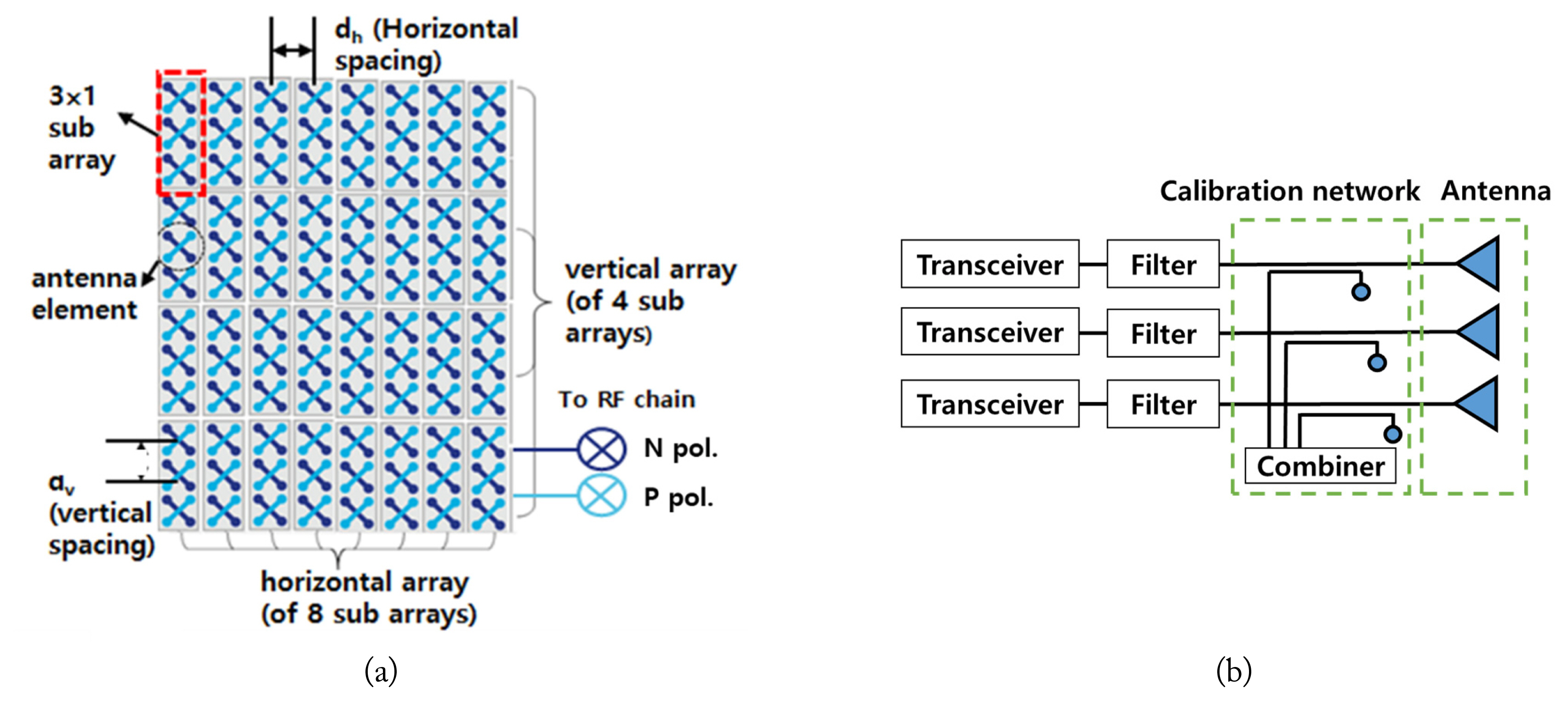
Fig. 1 presents an example of the antenna configuration of an active antenna system for a massive MIMO. In terms of the development cost and angular coverage of the cell, applying independent digital beamforming to every antenna element would be inefficient. Hence, a single transmit/receive chain, including a power amplifier and a low-noise amplifier, is connected to a group of antennas, called a subarray. The subarray consists of three antenna elements, with each antenna element having two polarizations—positive polarization (P pol.), which is tilted by +45° relative to the vertical axis, and negative polarization (N pol.), which is tilted by −45°. Since a signal input is necessary for each polarization, each subarray bears two input ports. Therefore, an entire array antenna comprises multiple subarrays as its array element. In particular, four vertical columns of subarrays and eight horizontal rows of subarrays create the entire array. Fig. 1(b) shows the configuration of a simple radio structure in AASs, which is connected to an antenna. The active antenna system is composed of 64 transceiver chains, each of which should deliver a precise and stable amplitude and phase to the antenna in various environments to create the desired beam-forming pattern. Furthermore, the calibration network serves to calibrate the amplitude and phase of the signal transmitted to the antenna.
In recent years, increasing demand for broadband dual-polarized antennas characterized by a compact and planar configuration has been observed, owing to their low cost, ease of manufacturing, and system integration. To address this demand, many dual-polarized base station antennas have been proposed to achieve broadband and dual-polarization performance, including antennas that involve modifying the dipole structure [4–6] and patch antennas using an L-probe feed and a meander line feed [7–11]. Notably, a double-layered stacked patch antenna has also been proposed in the literature for attaining a broad impedance band and flat gains [12]. Although these antennas exhibit broadband characteristics, they tend to have high antenna height and a mechanically complex structure—features that discourage mass production—since most of them have been produced with a focus on the performance of a single antenna element.
In this regard, liquid crystal polymers (LCPs) with low dielectric constant and low loss tangent have been proposed for use in circuit devices, module packaging, and flexible antenna arrays [13, 14]. Notably, LCPs are attractive materials for use in antennas due to their low water absorption and low dielectric losses.
In this paper, a novel low-profile, broadband, dual-polarized antenna structure is proposed for low cost and easy manufacturing of large-scale AASs for base stations. The proposed antenna is composed of 96 antenna elements with dimensions of 360 mm × 930 mm × 10 mm. Furthermore, a low-loss LCP-based plastic molding substrate is employed to easily fabricate a 3D fixture for the flexible 3D design of the antenna and feed line, as well as to reduce costs for fabricating two subarray-based molding modules compared to the costs involved in using a large-scale printed circuit board (PCB) substrate.
The proposed antenna operated efficiently in the C-band from 3.7 to 3.98 GHz. Furthermore, its performance was verified by comparing simulation results. The verification results confirmed that the novel plastic molding structure proposed in this study can be employed for the mass production of large-scale antennas, thus satisfying the cost reduction requirements as compared to antennas based on PCB.
II. 3 × 1 Subarray on Plastic Molded Module
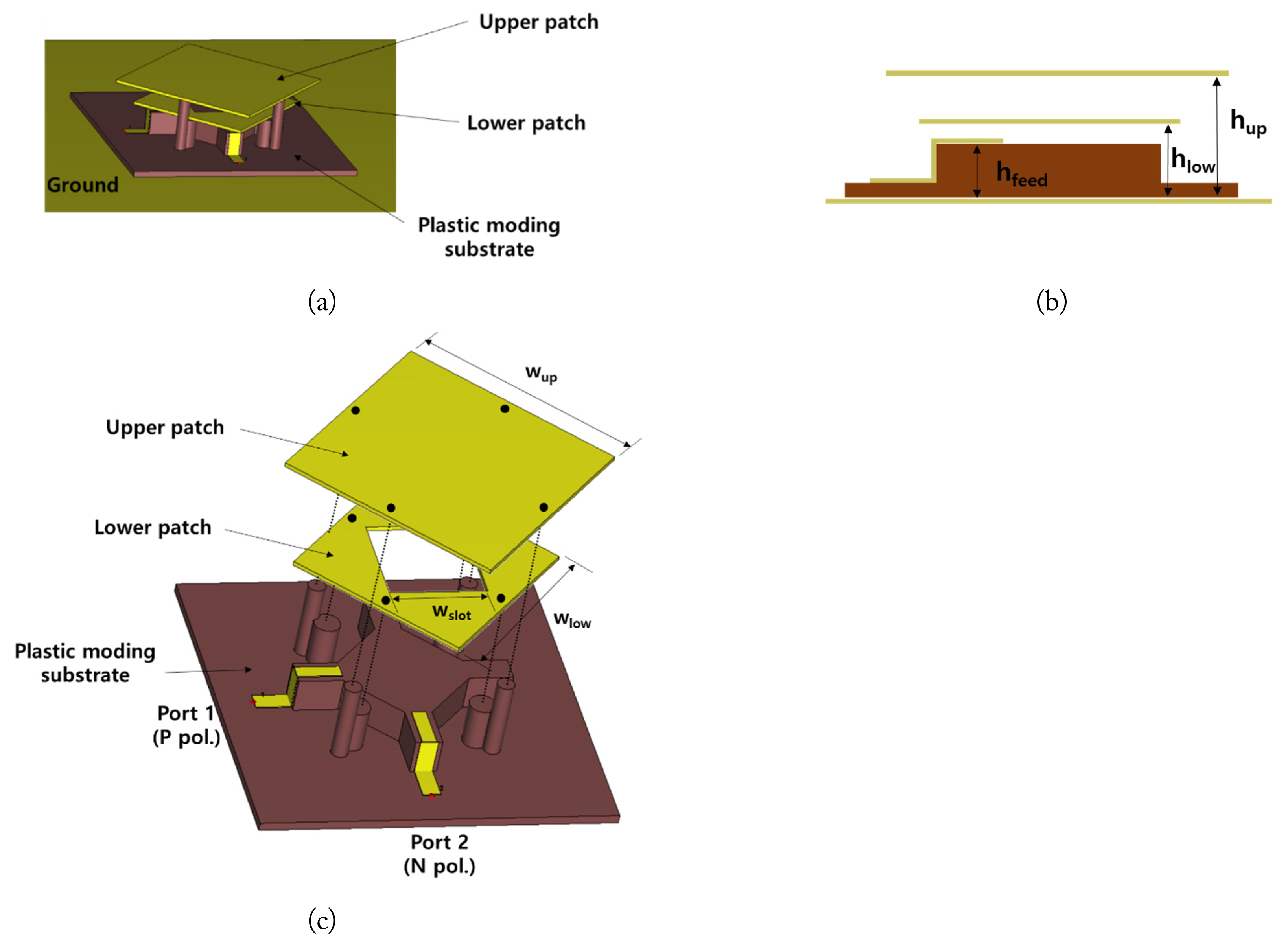
A basic plastic molding antenna element for large-scale MIMO systems at 3.7 GHz is presented in Fig. 2. A single antenna element consists of two stacked patches—a lower patch and an upper patch—that are floated on a plastic molding substrate while maintaining a constant gap between the lower stacked L-shaped coupled feed. The stacked patches were used to obtain a wide impedance bandwidth, which was satisfied when the upper patch was sufficiently floated from the lower patch for loose coupling. Furthermore, two resonant frequencies were placed closely to achieve wideband impedance using a relatively thick antenna.
When the distance between the upper and lower patches was decreased to lower the height of the antenna, strong coupling was observed, resulting in a wider separation between the two resonance frequencies. This led to some frequency regions between the two resonance frequencies failing to meet S11 < −10 dB. To address this issue, this paper proposes a structure in which a slot is made in the lower patch to reduce coupling while also narrowing the distance between the upper and lower patches. The length and width (wup) of the upper patch in Fig. 2(c) are 26 mm, while those (wlow) of the lower patch are 21 mm. Furthermore, the size (wslot) of the hole in the lower patch is 11 mm. The upper patch and lower patch are located 10 mm and 6 mm above the ground, respectively, while the feed is placed 5 mm above the ground. The upper and lower patches are supported by a plastic mold while also keeping an air gap between the patches. The feed line is raised 12 mm away from the center of the antenna, with the length of the feed line coupled with the lower patch being 5 mm.
The LCP material, which was used as the primary material for constructing the plastic structure, acted as a position fixture, as well as the substrate of the antenna and the feed line. This material was chosen because it allowed relatively easy fabrication of molding for mass production, was characterized by good thermal management in the molding process, and exhibited low loss characteristics for high radio frequency (RF) performance, such as insertion loss and antenna efficiency, as shown in Table 1.
Furthermore, compared to conventional fabrication processes based on large-scale PCBs for large-sized antennas, the proposed module has a relatively small size and could be repeatedly assembled on the metal ground to from a large-scale antenna.
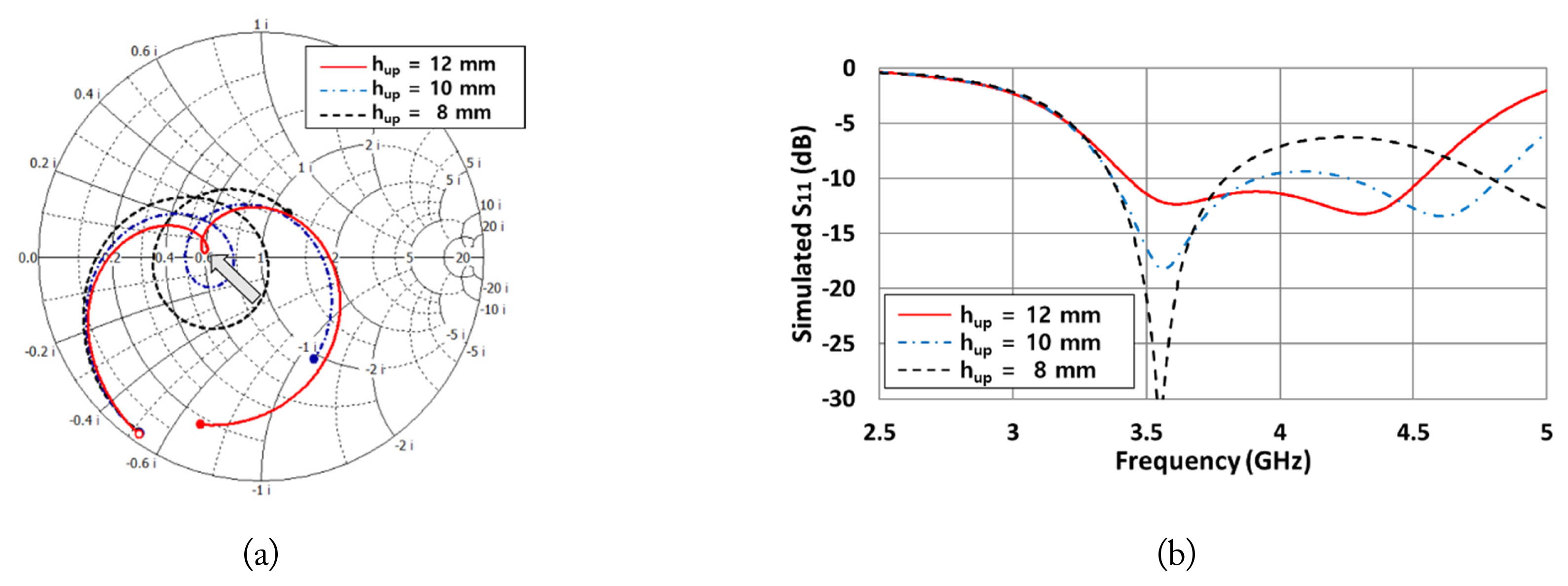
In the absence of a hole (wslot = 0) in the lower patch of the structure depicted in Fig. 2, the input impedance is simulated based on the height of the upper patch. Fig. 3(a) shows a Smith chart, while Fig. 3(b) depicts the magnitude of S11 with respect to frequency. It is evident that as the height of the upper patch increases, the coupling between the upper and lower patches decreases, ultimately leading to a reduction in the size of the resonance circle formed on the Smith chart. Additionally, the second resonant frequency declines as the coupling decreases. When the two resonance frequencies are located close to each other, an S11 < −10 dB is obtained over the entire frequency band. Therefore, although increasing the height of the upper patch is favorable from the perspective of bandwidth, it results in the disadvantage of thickening the antenna.
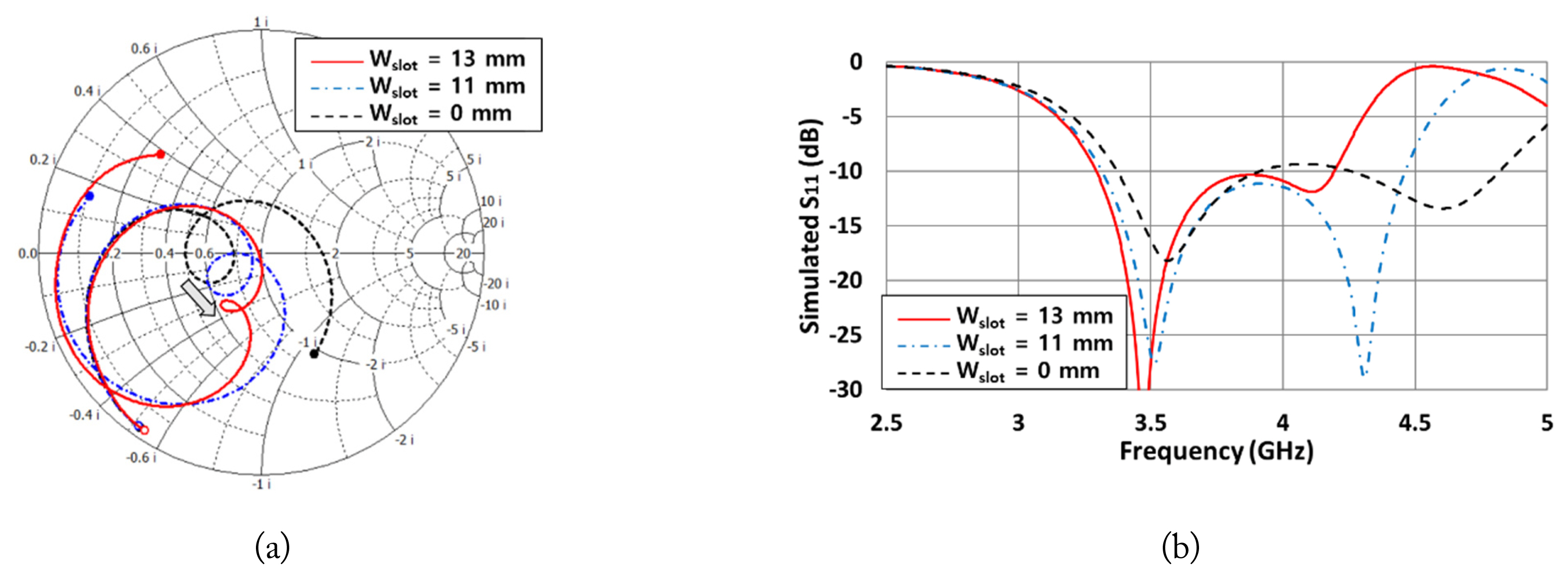
To reduce coupling without increasing the thickness of the antenna, a hole was introduced in the lower patch. The simulated S11 values when using varying hole sizes (wslot) for the same antenna structure as in Fig. 2 are presented in Fig. 4. As shown in Fig. 4(a), an increase in hole size leads to a decrease in coupling, resulting in a smaller resonant circle on the Smith chart. Additionally, Fig. 4(b) shows that the second resonant frequency also declines as the hole size increases. This indicates that the introduction of holes in the lower patch results in reduced coupling with the upper patch without having to increase its height. The shift in the position of the resonance circle on the Smith chart occurs because increasing the hole size in the lower patch leads to a lowering of the patch’s resonant frequency. In this context, impedance matching and other related factors can also be optimized by adjusting the length of the L-probe. The S11 of the proposed antenna is traced by the blue dash-dotted line in Fig. 4, achieving a 1.14 GHz (3.32–4.46 GHz) impedance bandwidth.
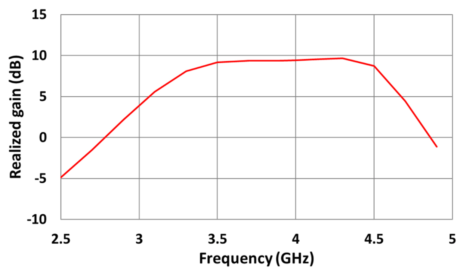
Fig. 5 illustrates the simulated realized gain in terms of different frequencies. Within the impedance bandwidth of 3.32–4.46 GHz, the antenna gain varies between a minimum of 8.1 dBi and a maximum of 9.5 dBi. Moreover, the antenna gain over various frequencies reveals considerable wideband performance for a single element.
To enrich the distribution of the radiated power within the coverage area and to reduce interference from the upper region, a 6° electronically down-tilt beam is required in the vertical direction of the base station antenna. For a 6° down-tilt beam in the vertical direction, the phase difference at each feed network for a subarray should be about 36°. Notably, a 3 × 1 subarray in the vertical direction would be more efficient than using three single antennas for independent digital beamforming and RF chains even the vertical beamforming range of the antenna is limited to a specified range.
When determining the distance between the vertical antennas, the vertical beamforming range and increment of gain should be carefully considered as the main specifications of the active antenna system. For the system proposed in this study, the distance between antennas in the vertical direction was 0.78λ (61 mm) for a vertical scan range of 20° and a gain of approximately 11 dBi. Meanwhile, the distance between antennas in the horizontal direction was 0.54λ (42 mm). Notably, a 3 × 1 subarray can support two polarizations—P pol. and N pol. Therefore, two signal lines supporting these two polarizations of the 3 × 1 subarray antenna were connected using the transmit/receive RF chain.
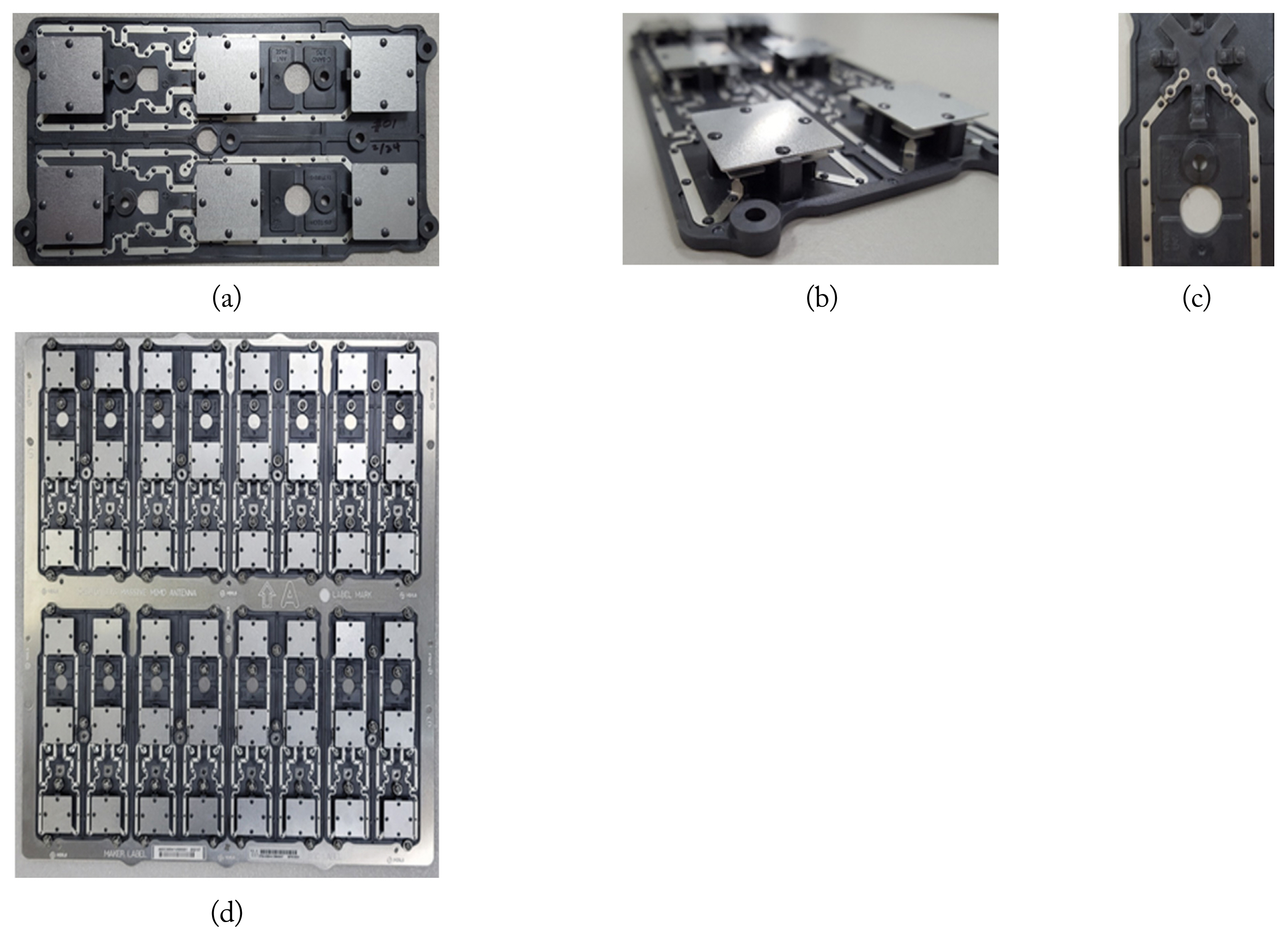
The size of the module, composed of two 3 × 1 subarrays, was determined by accounting for the productivity of the molding process and the efficiency of assembling it on metal ground. Furthermore, the 3 × 1 feed lines were created by cutting aluminum sheets of 100 μm thickness, which were then attached to the plastic fixture using specific melting structures, as shown in Fig. 6.
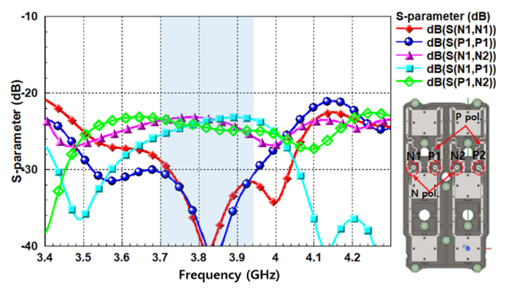
Fig. 7 shows the simulated S-parameters of the two 3 × 1 subarrays. S(N1,N1) refers to the S11 of the N pol. port, while S(P1,P1) denotes the S11 of the P pol. port. Furthermore, S(N1,N2) refers to the co pol. isolation between ports N1 and N2, while S(N1,P1) is the self-cross pol. isolation between ports N1 and P1. Finally, S(P1,N2) indicates the cross-pol. isolation between ports P1 and N2. The S11 of the two polarizations satisfied the −20 dB specification and port isolation. Furthermore, polarization isolation between the two ports of the antennas was at least under −21 dB within the concerned frequency band. Notably, the broader impedance bandwidth achieved by the sub-array antenna compared to a single antenna can be attributed to the influence of the feeding structure.
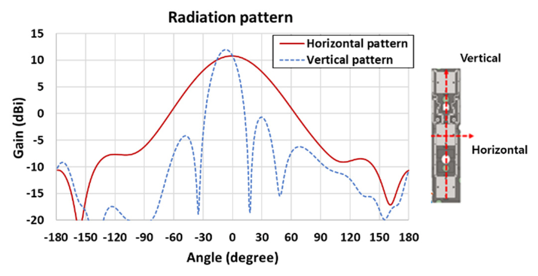
Fig. 8 traces the simulated antenna patterns of the 3 × 1 subarray supporting P pol. Notably, the pattern of N pol. was found to be similar to that of P pol., since the feeding point was structurally symmetric. Furthermore, the 3 dB beam-width of the horizontal pattern was approximately 61°, while the gain of the subarray was 10.7 dBi. Similarly, the 3 dB beamwidth of the vertical pattern was 20° with a 6° fixed down-tilt angle, while the peak gain was 11.7 dBi. This indicates that the scanning range of the entire active antenna system can be accurately estimated from the subarray beam pattern.
III. Radiation Patterns of the Active Antenna System
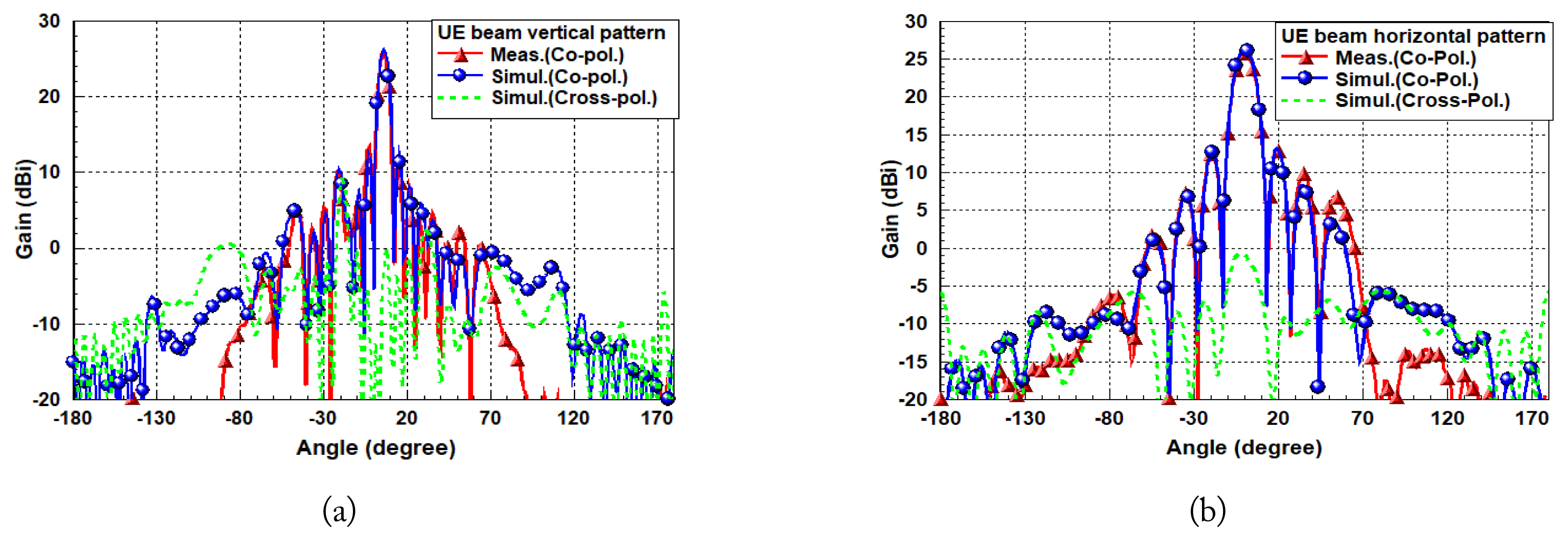
Each input port of the subarray antenna was connected to beamforming integrated circuits (ICs). A user-specific beam was transmitted toward the individual receive antenna of the user through a beamforming weight vector, defined as a steering vector toward the user’s direction in line-of-sight (LOS) conditions or a maximal ratio transmission vector in non-LOS environments. In LOS conditions, the array gain was observed to be equal to the number of subarrays. The maximum antenna gain of the user-specific beam can be expressed in dB as the sum of its array factor and the subarray gain. Notably, the array factor is usually proportional to the number of subarrays in an array, while the subarray gain is approximately proportional to the number of antenna elements within a subarray (3 × 1 subarray) and the spacing between adjacent subarrays (4 × 8 system). The antenna gain toward the boresight of the proposed active antenna system was estimated to be approximately 25.7 dBi when considering two factors—gains of the array factor (15 dB) and the subarray (10.7 dBi). Fig. 9 shows the simulated and measured patterns of the user-specific beam of the proposed active antenna system at boresight, exhibiting maximum gain in the azimuth and vertical directions at 3.7 GHz. The 3 dB beamwidth was approximately 12° in the azimuth direction and 5° in the vertical direction. Notably, the measured beam pattern and gain were similar to the simulation results obtained at boresight. The antenna efficiency was almost above 91%, including the feedline loss from a low-loss LCP-based substrate.
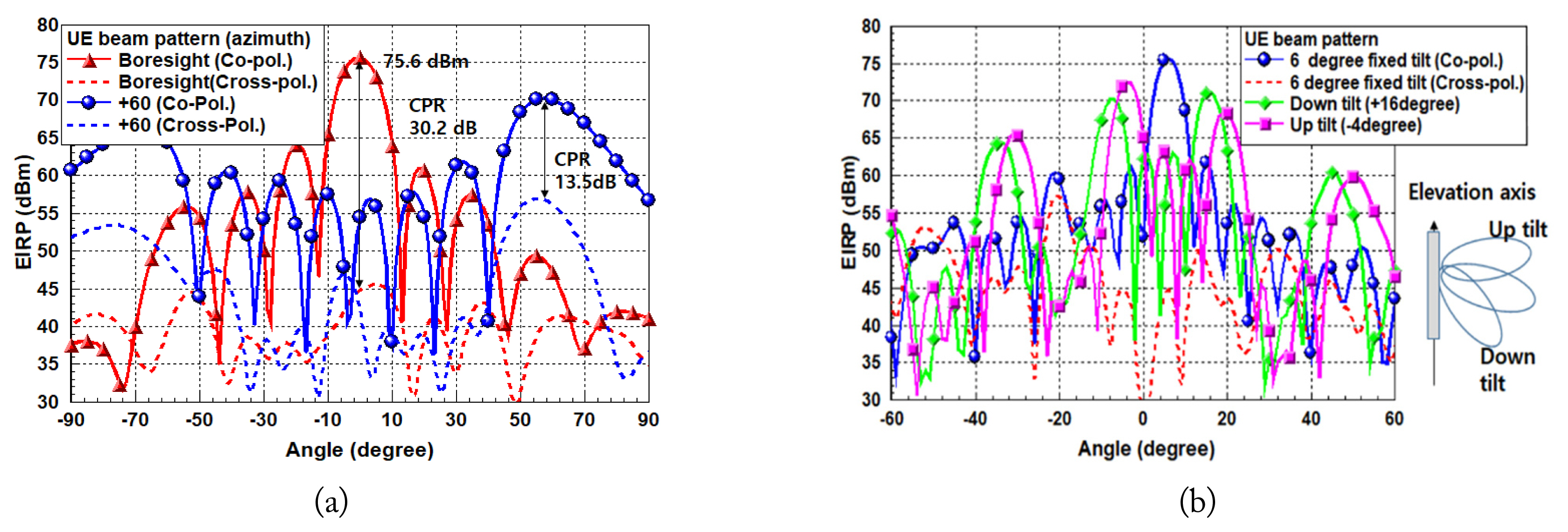
The set-level, user-specific beam performance of the proposed active antenna system with maximum tilting range in the azimuth and elevation axes was measured, as shown in Fig. 10. The measured peak effective isotropic radiated power (EIRP) was 75.6 dBm, while the scanning range was 120° from −60° to 60° in the azimuth axis. The tilting range was approximately 20°—from +16° down-tilt angle to −4° up-tilt angle—along with the 6° fixed-tilt angle achieving maximum gain in the vertical axis. The cross-polarization ratio level—the ratio between co-polarization and cross-polarization—was 30.2 dB at boresight and 13.5 dB at the 60° scanning angle. Therefore, the beamforming performance of the proposed structure, including the performance of the system elements, such as antennas, RF transceivers, and other related functions, can be expected to satisfy the beamforming performance of commercial base stations.
Table 2 compares the performance of the antenna proposed in this paper with existing references [7–9, 15–18]. It is observed that the resonance frequency of the references is below 2 GHz, while their antennas were designed with a height of at least 17 mm. Additionally, while antennas designed for the 3.7 GHz band has a lower height compared to the proposed antenna, they still fail to reach a bandwidth as wide as that attained in this paper.
IV. Conclusion
This study investigated a novel low-cost antenna fabrication and assembly solution for large-scale AASs. The proposed antenna comprises over 96 antenna elements at 3.7 GHz, and involves repeatedly assembling an LCP-based plastic module using an attachable 3 × 1 feed line. In addition, a low-profile wideband antenna with stacked patch antennas was obtained, even with loose coupling between the upper and lower patch antennas, by perforating the inner patch antenna. Subsequently, the proposed structure was verified to satisfy a wide impedance bandwidth of 1.14 GHz within a height of 10 mm. Furthermore, set-level beamforming measurements of the active antenna system with 64-chain (4 × 8 array and two pol.) transceivers were verified, exhibiting a maximum EIRP of 75.5 dBm at boresight and a steering range of <±60° in the azimuth axis. Overall, the proposed solution can be considered a suitable candidate for use in commercial active antenna system-based base stations with large-scale arrays at 3.7 GHz.