 |
 |
- Search
| J. Electromagn. Eng. Sci > Volume 24(3); 2024 > Article |
|
Abstract
To achieve simple and reliable conversion from constant current (CC) charging mode to constant voltage (CV) charging mode in wireless power transfer systems, this paper proposes a hybrid topology equipped with a reconfigurable rectifier. An AC switch is adapted to simultaneously realize the change from half-bridge rectification to full-bridge rectification and achieve the shift from a topology with capacitors in the series compensated primary and secondary sides to a topology with capacitors in the series compensated primary side and the inductor-capacitor-inductor (LCL) compensated secondary side. Notably, communication between the transmitter and receiver sides is not necessary in the proposed method. Furthermore, the zero phase angle characteristic is successfully maintained in both charging modes. The experimental results obtained using the 48 V/0.7 A experimental prototype, which was built to validate the relevant theoretical analysis, show that output current/voltage can be achieved in CC/CV charging mode independent of load resistance. Notably, the maximum power transfer efficiency of the system during the charging process reached 95.33%.
Wireless power transfer (WPT) technology has the potential to effectively enhance the freedom and security of a power supply approach. It has been widely used in electric vehicles, rail transit, implantable medical devices, industrial equipment, consumer electronics, power system monitoring equipment, and other fields [1–8]. In general, lithium-ion batteries have been chosen as the power source for several types of electrical equipment. To enhance the safety and efficiency of battery charging, a typical charging process can be divided into two stages—constant current (CC) charging mode and constant voltage (CV) charging mode [9]. Notably, during the charging process, the equivalent resistance of the battery undergoes significant changes. This requires the charging current (voltage) in the CC (CV) charging mode to be independent of load resistance. In addition, zero phase angle (ZPA) characteristics, which are integral to the efficient operation of the system, should be maintained throughout the charging cycle.
Currently, most reported technologies for realizing CC and CV charging in WPT systems can be classified into two types. The first type involves using CC and CV control methods based on compensation topology invariance, such as phase shifting control, DC-DC converter, and frequency modulation control, as proposed in [10–13]. The output current or voltage is controlled by adjusting the phase-shifting angle of the inverter or the rectifier [10]. However, this method is prone to causing hard on/off for the switch and increasing power loss. Although these problems can be avoided by introducing a DC-DC converter to regulate the output voltage and current on the transmitter and receiver sides [11], the introduction of passive components could lead to additional power loss and create issues related to volume and weight. Notably, CC and CV charging modes can be realized at two system frequencies when considering a fixed compensation topology, indicating frequency modulation control. For instance, when using a topology with capacitors in the series compensated primary and secondary sides (S-S topology), the system produces not only the characteristic CC output at the resonance frequency point, but also two CV output frequencies that are either higher or lower than the resonant frequency [12]. These same characteristics were observed for LCC-LCC topology [13]. However, the variation in mutual inductance between the transmitter coil and the receiver coil may affect the CC or CV operating frequency points of the system, in turn reducing its reliability. Moreover, communication is indispensable to the above methods. The delay or interruption in communication inevitably influences the output characteristics of the WPT system.
As for the second type, CC and CV charging modes can also be achieved by switching two different compensation topologies [9, 14–16]. When two different topologies exhibit CC and CV output characteristics at the same resonant frequency, the changing over of the charging mode is realized by switching one or more of the AC switches. For instance, Qu et al. [9] proposed hybrid topologies using either series-series (SS) and series-parallel (PS) compensation or parallel-series (PS) and parallel-parallel (PP) compensation to realize CC and CV charging modes, achieving conversion from CC to CV charging mode using AC switches. This topology involved one inductance and three additional AC switches. Furthermore, a hybrid inductive power transfer battery charger combining LCC-LCC and LCC-S topologies was presented in [17]. The LCC-LCC compensation topology was utilized to provide the configurable CC output, while the LCC-S compensation network was employed to realize the configurable CV output. Two extra power switches were used to change the operation mode. However, in the case of the charging mode transition from CC output to CV output, an inductor on the receiver side became redundant, causing additional power loss.
This paper proposes a novel hybrid topology consisting of a reconfigurable rectifier. An AC switch is employed to facilitate the switching of the rectifier operating modes and compensation topologies, and also to enable the system to switch from CC charging mode to CV charging mode. At the same time, the proposed method does not require communication between the transmitter and receiver sides, which is beneficial for the simple and reliable operation of WPT systems.
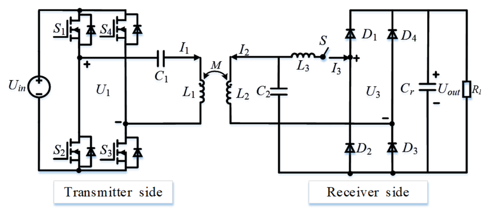
Fig. 1 presents the proposed WPT system with a reconfigurable rectifier, where S1–S4 denote four MOSFETs and D1–D4 are four diodes. L1 and L2 represent the inductance of the transmitter and receiver coils, respectively. Furthermore, C1 is the compensation capacitor on the transmitter side, while C2 and L3 are the compensation capacitor and compensation inductance on the receiver side, respectively. Cr refers to the filter capacitor on the rectifier while RL is the load resistance.
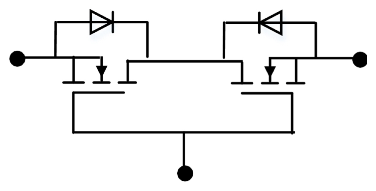
In addition, S is an AC switch composed of two anti-series connected MOSFETs on the receiver side, as shown in Fig. 2.
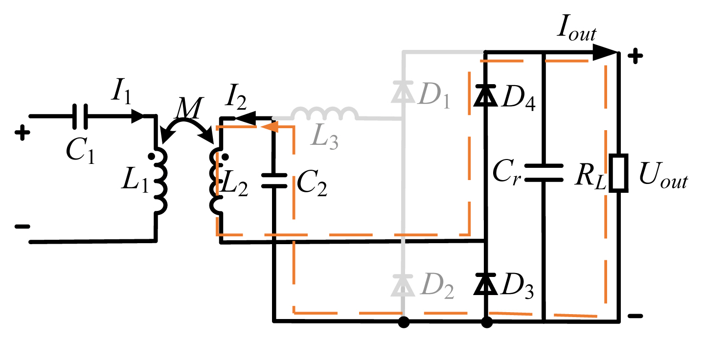
The switch S not only controls the operating mode of the rectifier but also dominates the charging mode of the WPT system. The simplified circuit diagram of the system when S is turned off is depicted in Fig. 3, where the rectifier of the proposed WPT system works in the half-bridge rectifier (HBR) mode. The dotted line indicates the direction of the current flow on the receiver side. In HBR mode, C1 and C2 together form an S-S compensation network for the WPT system. Notably, the equivalent AC load of the HBR and battery load can be expressed as follows [18]:
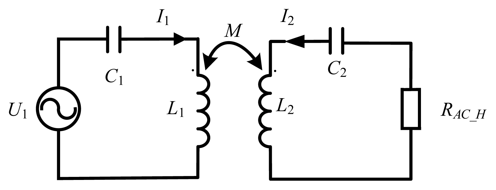
Furthermore, according to the fundamental harmonic approximation method, the equivalent AC circuit of the HBR in Fig. 3 can be structured as shown in Fig. 4.
Subsequently, drawing on Kirchhoff voltage law (KVL), the following equation was obtained:
When the operating frequency of the system becomes the resonant frequency—i.e., it is satisfied—the input current and output current can be expressed by drawing on Eq. (2), as follows:
As evident in Eq. (3), since the output current is independent of load resistance in HBR mode, CC charging can be achieved. The input impedance of the WPT system in the HBR mode can be expressed as:
Ultimately, based on Eq. (4), the ZPA operation in the CC charging mode was obtained.
A simplified circuit diagram of the system when switch S is turned on is shown in Fig. 5. Notably, the rectifier of the proposed WPT system works in full-bridge rectifier (FBR) mode.
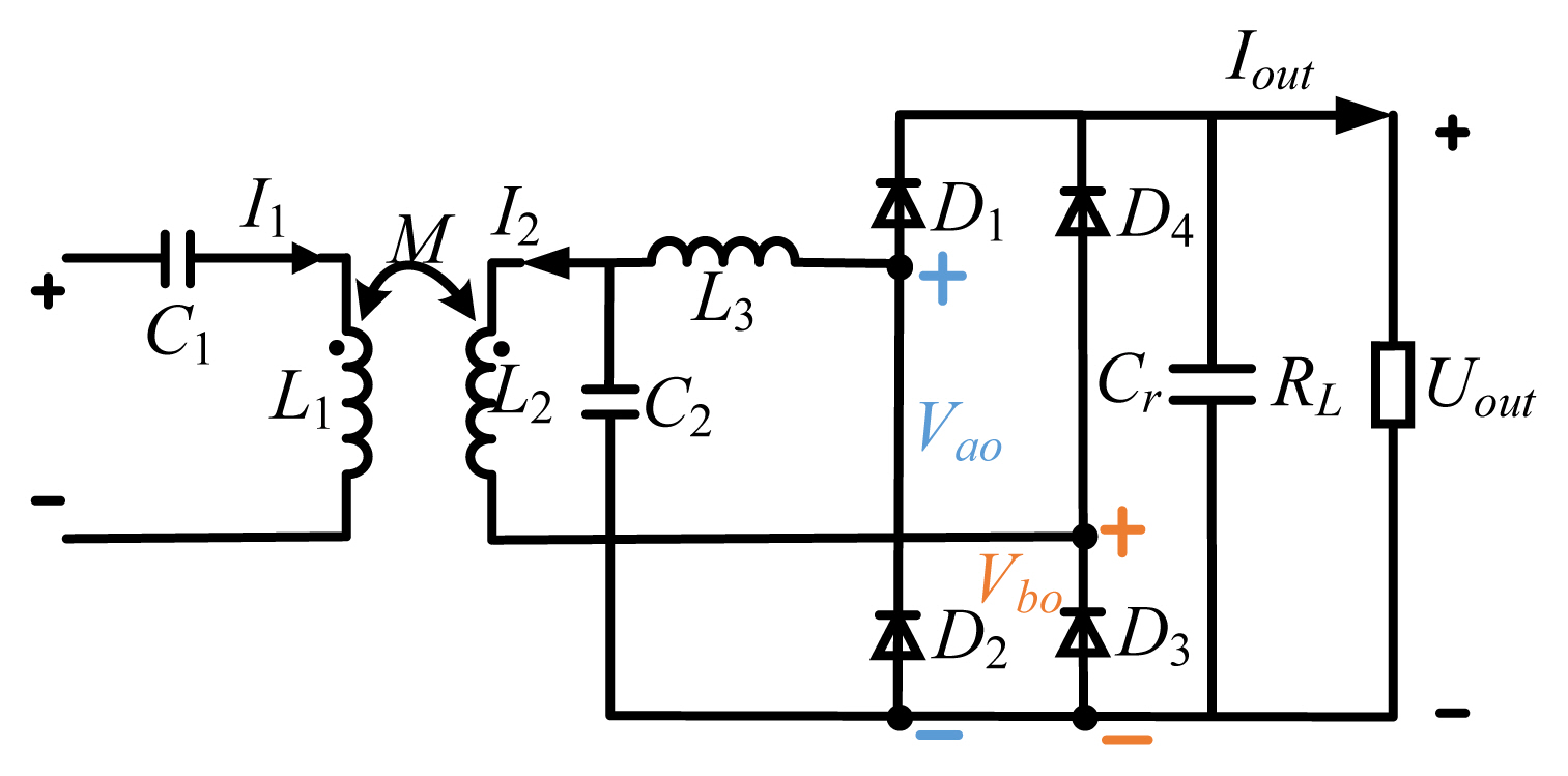
As shown in Fig. 5, when the rectifier operates in FBR mode, it performs equivalently to two HBRs connected parallelly, with the voltage of the battery determined by the higher value of |Vao| and |Vbo| [19]. When |Vao| > |Vbo|, diode D4 is clamped and D3 is conducted. After the current flows through D1 and the load from L3, some of it flows through L2 and back to L3, while the other part flows back to L3 from C2. Notably, D2 refers to the freewheeling diode, as shown in Fig. 6(a). Similarly, when |Vao| < |Vbo|, diode D1 is clamped and D2 is turned off. As a result, the current flows through the load from D4, where D3 is the free-wheeling diode, as shown in Fig. 6(b).
Subsequently, the equivalent AC circuit of the FBR mode can be structured the same way as shown in Fig. 7.
In Fig. 7, RAC_F1 and RAC_F2 vary with changes in the load voltage. The relationship between RAC_F1, RAC_F2, and RL can be expressed as follows [19]:
When the load voltage exceeds a certain rated value, the working mode of the system switches from Fig. 6(a)–6(b), with the equivalent AC circuit being the one depicted in Fig. 4. This may also be regarded as the branch disconnection of I3 in Fig. 7, the detailed discussion for which has been presented in following section. Using KVL, the following equation was obtained:
When the system operating frequency becomes the resonant frequency, i.e., jωL1+1/jωC1=jωL2+1/jωC2=0 and L2 = L3 are established, the current flow through each inductor can be formulated by drawing on Eq. (6), as follows:
Furthermore, the voltage of the equivalent AC load of the FBR and battery load Vao and Vbo can be calculated as follows:
Combining Eq. (8), it is evident that when |Vao| > |Vbo|, CV charging mode can be achieved. In CV charging mode, the voltage across Cr does not change suddenly. Moreover, the input impedance in the FBR mode can be expressed as follows:
Furthermore, this study calculated the ZPA operations in CV charging mode using Eq. (9). However, as evident from Eq. (8), an increase in load resistance would cause |Vbo| > |Vao| to no longer hold true. In other words, when the load resistance value exceeds a critical value, the system would no longer operate in CV mode. In Eq. (8), assuming that Vao is equal to Vbo, then RAC_F2=ωL2 can be obtained. Moreover, when |Vbo| > |Vao|, the diodes D1 and D2 would be clamped. Subsequently, the state of the circuit will return to the FBR mode and its equivalent circuit model, as shown in Fig. 4, where RAC_F2=RAC_H. Drawing on the above discussion, the following conditions can be obtained using the following equation:
Notably, for WPT systems that operate in the standard frequency band for commercial use, the critical resistance RL_cr usually exceeds several hundred ohms—a value that is difficult to reach when considering the internal resistance of the battery. Thus, a |Vbo| > |Vao| situation is not considered in the following discussions in this article.
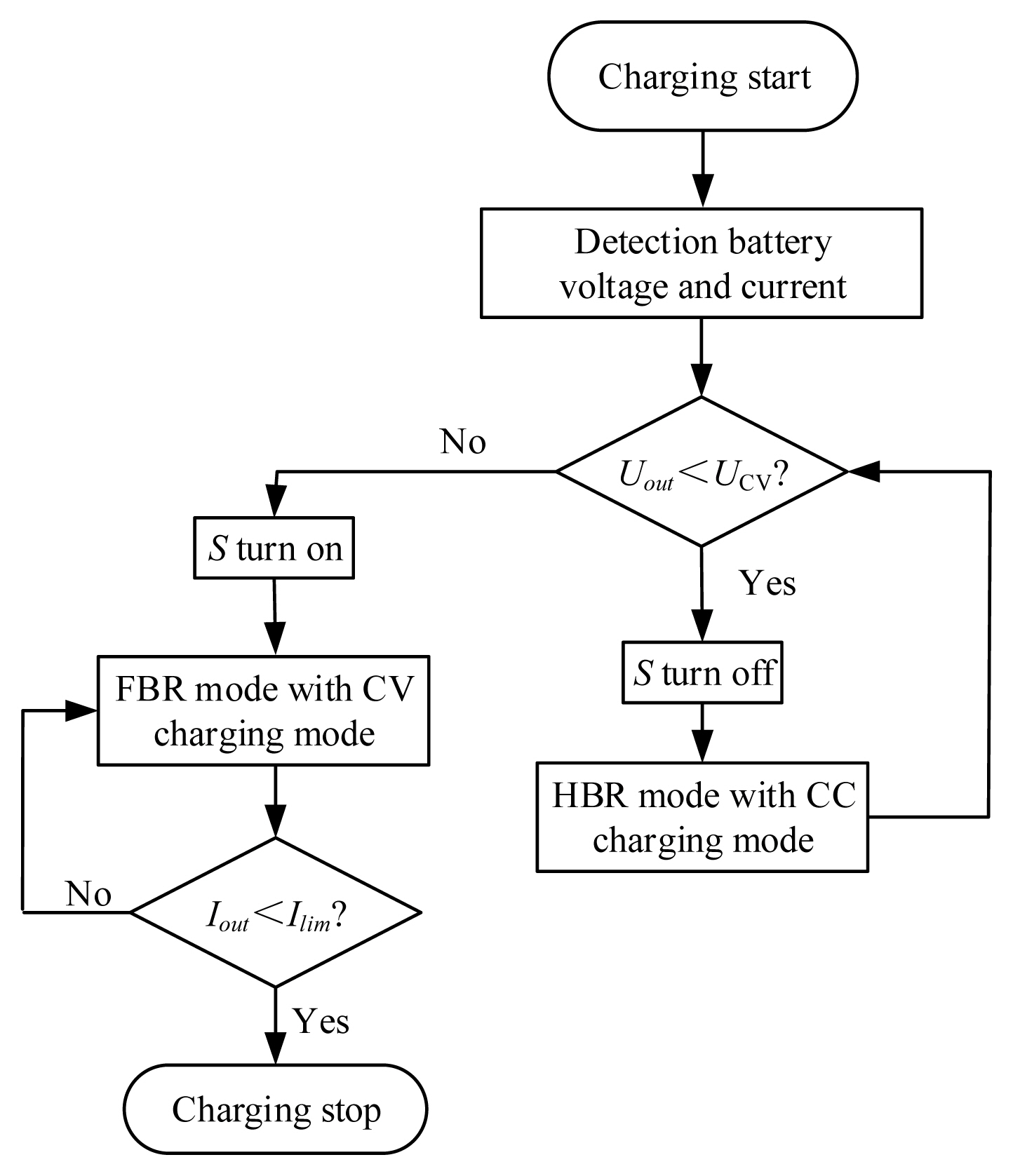
A control flowchart of the proposed WPT system for CC/CV charging is presented in Fig. 8. When the process of charging begins, switch S remains turned off, during which the rectifier works in HBR mode and the WPT system works in CC charging mode. Subsequently, when the load voltage Uout is detected to be greater than the preset voltage UCV, switch S is turned on. As a result, the WPT system starts working in CV charging mode using FBR mode. Lastly, the charging process concludes when the load current is finally less than the preset current Ilim.
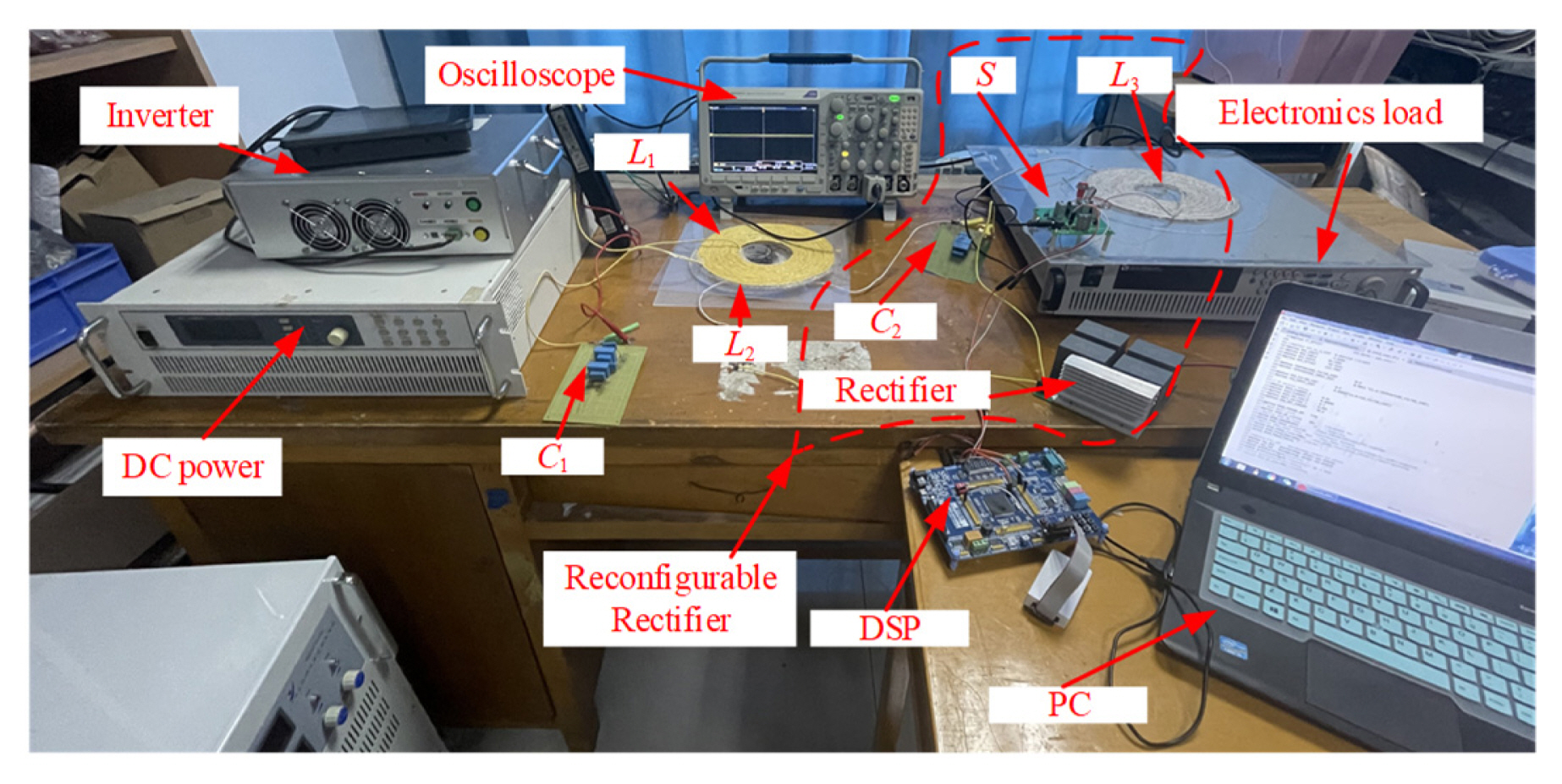
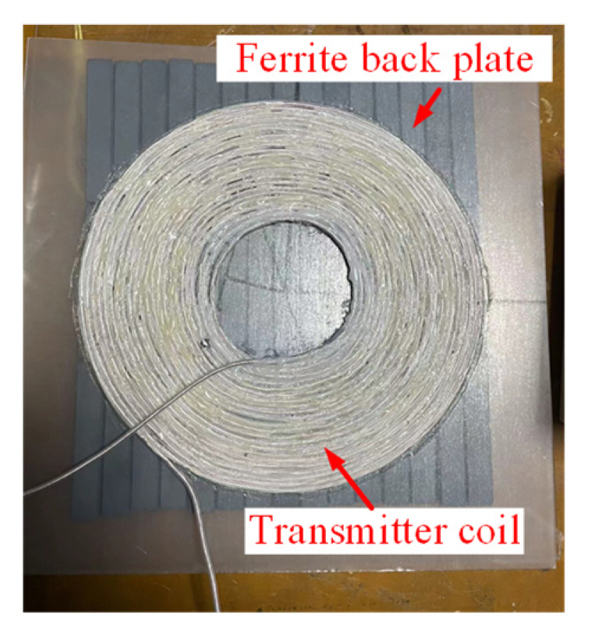
To validate the feasibility and superiority of the theoretical analysis demonstrated in the previous section, a 48 V/0.7 A experimental prototype was designed and then fabricated, as shown in Fig. 9. The four MOSFETs are the GS66508B located on the inverter, while the four diodes used on the reconfigurable rectifier are IV1D12030U3. Notably, the variation in load resistance was simulated using an electronics load. Fig. 10 shows a photograph of the magnetic coupler of the transmitter coil, along with a ferrite black plate (PC40). Furthermore, the specific parameters are represented in Table 1. To ensure the accuracy of the compensation inductance L3, it was given the same winding as the receiver coil and was placed at a considerable distance from the magnetic coupler.
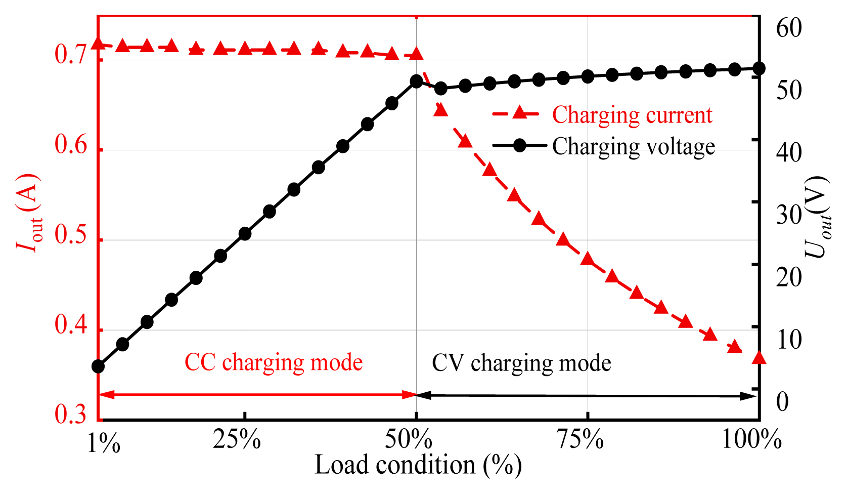
At the beginning of the charging process, the system works in the CC charging mode. When battery resistance reaches 50% load condition, the system switches from CC charging mode to CV charging mode, and continues to maintain the CV charging mode until the end of the charging process.
As shown in Fig. 11, the fluctuation percentage of the charging current in CC charging mode is less than 1.6% (0.717–0.705 A) while that of the charging voltage in CV charging mode is below 6.2% (48.21–51.42 V). This indicates that the proposed WPT system with a reconfigurable rectifier maintains agreeable CC/CV output characteristics throughout the charging process. Fig. 12 traces the waveforms of the input voltage U1 and input current I1 at different load conditions in the CC charging mode.
Fig. 12(a) and 12(b) show that changes in the load condition do not affect the input impedance angle between input voltage U1 and input current I1. Furthermore, the ZPA characteristics in the CC charging mode were verified. Fig. 13 presents the waveforms for load voltage Uout and load current Iout in the CC charging mode at the moment when the load resistance is switched from a 25% load condition to a 50% load condition.
It is evident that at the moment of load resistance switching, the load current re-attains its original value after a brief decrease, while the load voltage increases by half. A similar analysis was conducted for the CV charging mode, as shown in Figs. 14 and 15.
Furthermore, the ZPA characteristic in the CV charging mode was verified, the results of which are shown in Fig. 14. Notably, a change in load condition did not influence the input impedance angle between input voltage U1 and input current I1. Fig. 15 depicts the load voltage and load current waveforms in the CV charging mode on switching the load resistance from a 50% load condition to a 100% load condition. It is observed that the load current decreases by half, while the load voltage undergoes a slight change, only to subsequently return to a constant value.
As observed in Fig. 16, the power transfer efficiency of the entire charging process was successfully maintained above 86.23%. In the CC charging mode, the power transfer efficiency increased gradually with an increase in the load condition, with the maximum power transfer efficiency being 95.33%. Similar to the CC charging mode, the power transfer efficiency in the CV charging mode climbed from 88.76% to 94.28% with an increase in the load condition.
Table 2 provides an overview of a few of the typical methods currently used for implementing CC/CV charging modes, including their performance [9, 13, 20]. Compared to previous related studies, the method proposed in this paper offers marked improvements, such as fewer passive components and two charging modes achieved using only one AC switch at a fixed system frequency, which effectively reduced the difficulty of system control as well as system losses caused by the additional introduction of devices.
Furthermore, all the controls were based on the secondary side, while the communication module could be avoided entirely. Hence, the proposed method is extremely suitable for scenarios in which communication between the primary and secondary sides is unstable, such as underwater or mine applications.
This paper proposes a hybrid topology equipped with a reconfigurable rectifier for WPT systems. An AC switch is adapted to realize the change from the CC charging mode to the CV charging mode. When the switch is turned off, the rectifier operates in the HBR mode in conjunction with the S-S type compensation at the pre-stage, thus implementing the CC charging mode. In contrast, when the switch is turned on, the rectifier operates in the FBR mode, due to which the compensation structure of the system shifts to attain the S-LCL type, which then exhibits CV output characteristics. Notably, the ZPA condition could be maintained in both charging modes. In addition, the communication between the transmitter side and the receiver side could be eliminated in the proposed method. Furthermore, the experimental results show that fluctuations in charging current due to load condition changes in the CC charging mode can be maintained below 1.6%. For the CV charging mode, the fluctuations in charging voltage due to load resistance variation were less than 6.2%. Furthermore, during the charging cycle, power transfer efficiency was maintained above 86.23% throughout the process, with the maximum power transfer efficiency of the system reaching 95.33%. Overall, both the theoretical analysis and experimentation validate that the proposed hybrid WPT topology equipped with a reconfigurable rectifier exhibits agreeable CC/CV output characteristics throughout the charging process.
Acknowledgments
This work was supported in part by the National Natural Science Foundation of China (No. 52301403 and No. 52171338), in part by the China Postdoctoral Science Foundation (No. 2021M702638), and in part by the Natural Science Basic Research Plan of Shaanxi Province in China (No. 2023-JC-QN-0475).
Fig. 12
Waveforms of input voltage U1 and input current I1 in CC charging mode: (a) 25% load condition and (b) 50% load condition.

Fig. 13
Waveforms of load voltage and current at the moment of load resistance switching in CC mode.
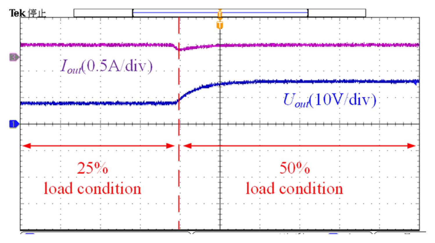
Fig. 14
Waveforms of input voltage U1 and input current I1 in CC charging mode: (a) 50% load condition and (b) 100% load condition.

Fig. 15
Waveforms of load voltage and current at the moment of load resistance switching in CV mode.
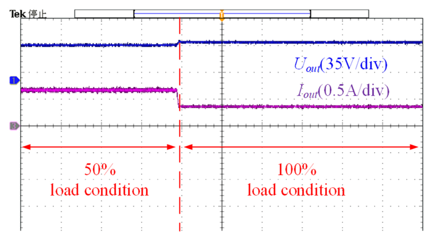
Table 1
System specifications and their designed parameters
Table 2
Comparison of the current work with previous related works
| Qu et al. [9] | Vu et al. [13] | Ji et al. [20] | This work | |
|---|---|---|---|---|
| CC/CV switching method | Topology switching | Frequency switching | Topology switching | Topology switching |
| Total number of passive components | 5 | 6 | 14 | 4 |
| Communication | Yes | Yes | No | No |
| Total number of AC switches | 3 | 0 | 1 | 1 |
| Max DC-DC efficiency (%) | 93.00 | 96.10 | 88.65 | 95.33 |
References
1. N. Ha-Van, H. Le-Huu, M. Thuy Le, K. Park, and C. Seo, "Free-positioning wireless power transfer using a 3D transmitting coil for portable devices," Journal of Electromagnetic Engineering and Science, vol. 20, no. 4, pp. 270–276, 2020. https://doi.org/10.26866/jees.2020.20.4.270

2. A. U. Ibrahim, W. Zhong, and M. D. Xu, "A 50-kW three-channel wireless power transfer system with low stray magnetic field," IEEE Transactions on Power Electronics, vol. 36, no. 9, pp. 9941–9954, 2021. https://doi.org/10.1109/TPEL.2021.3064373

3. M. Budhia, J. T. Boys, G. A. Covic, and C. Y. Huang, "Development of a single-sided flux magnetic coupler for electric vehicle IPT charging systems," IEEE Transactions on Industrial Electronics, vol. 60, no. 1, pp. 318–328, 2013. https://doi.org/10.1109/TIE.2011.2179274

4. A. Alkasir, S. E. Abdollahi, S. Abdollahi, and P. Wheeler, "Analytical modeling of self and mutual inductances of DD coils in wireless power transfer applications," Journal of Electromagnetic Engineering and Science, vol. 22, no. 2, pp. 162–170, 2022. https://doi.org/10.26866/jees.2022.2.r.73

5. C. Xiao, K. Wei, D. Cheng, and Y. Liu, "Wireless charging system considering eddy current in cardiac pacemaker shell: Theoretical modeling, experiments, and safety simulations," IEEE Transactions on Industrial Electronics, vol. 64, no. 5, pp. 3978–3988, 2017. https://doi.org/10.1109/TIE.2016.2645142

6. J. Wang, H. Qu, B. Tao, C. Cai, Z. Lin, L. Xie, and F. Zhang, "Misalignment-tolerant integrated IPT systems for tram logistics robots featuring dual-purpose coupler," IET Electric Power Applications, vol. 14, no. 10, pp. 1984–1995, 2020. https://doi.org/10.1049/iet-epa.2020.0023

7. Q. Zhu, M. Su, Y. Sun, W. Tang, and A. P. Hu, "Field orientation based on current amplitude and phase angle control for wireless power transfer," IEEE Transactions on Industrial Electronics, vol. 65, no. 6, pp. 4758–4770, 2018. https://doi.org/10.1109/TIE.2017.2767556

8. G. Ning, K. Zhou, J. Liang, H. Wang, and M. Fu, "Reconfigurable and modular wireless charger based on dual-band design," IEEE Transactions on Circuits Systems II: Express Briefs, vol. 70, no. 9, pp. 3524–3528, 2023. https://doi.org/10.1109/TCSII.2023.3262245

9. X. Qu, H. Han, S. C. Wong, K. T. Chi, and W. Chen, "Hybrid IPT topologies with constant current or constant voltage output for battery charging applications," IEEE Transactions on Power Electronics, vol. 30, no. 11, pp. 6329–6337, 2015. https://doi.org/10.1109/TPEL.2015.2396471

10. C. S. Wang, O. H. Stielau, and G. A. Covic, "Design considerations for a contactless electric vehicle battery charger," IEEE Transactions on Industrial Electronics, vol. 52, no. 5, pp. 1308–1314, 2005. https://doi.org/10.1109/TIE.2005.855672

11. M. Fu, H. Yin, X. Zhu, and C. Ma, "Analysis and tracking of optimal load in wireless power transfer systems," IEEE Transactions on Power Electronics, vol. 30, no. 7, pp. 3952–3963, 2015. https://doi.org/10.1109/TPEL.2014.2347071

12. W. Zhang, S. Wong, C. K. Tse, and Q. Chen, "Load-independent duality of current and voltage outputs of a series or parallel compensated inductive power transfer converter with optimized efficiency," IEEE Journal of Emerging and Selected Topics in Power Electronics, vol. 3, no. 1, pp. 137–146, 2015. https://doi.org/10.1109/JESTPE.2014.2348558

13. V. B. Vu, D. H. Tran, and W. Choi, "Implementation of the constant current and constant voltage charge of inductive power transfer systems with the double-sided LCC compensation topology for electric vehicle battery charge applications," IEEE Transactions on Power Electronics, vol. 33, no. 9, pp. 7398–7410, 2018. https://doi.org/10.1109/TPEL.2017.2766605

14. J. H. Lu, W. J. Li, B. Li, and G. R. Zhu, "Variable compensation network for achieving constant current or voltage output in IPT system," In: Proceedings of the 2016 International Conference on Industrial Informatics-Computing Technology, Intelligent Technology, Industrial Information Integration (ICIICII); Wuhan, China. 2016, pp 14–17. https://doi.org/10.1109/ICIICII.2016.0015

15. C. Wang and J. Wang, "A hybrid LCC-SP compensation network with adjustable impedance angle used for single-stage wireless power transfer," IEEE Transactions on Transportation Electrification, vol. 9, no. 2, pp. 3452–3463, 2023. https://doi.org/10.1109/TTE.2022.3222869

16. Y. Zhang, Z. Shen, W. Pan, H. Wang, Y. Wu, and X. Mao, "Constant current and constant voltage charging of wireless power transfer system based on three-coil structure," IEEE Transactions on Industrial Electronics, vol. 70, no. 1, pp. 1066–1070, 2023. https://doi.org/10.1109/TIE.2022.3150112

17. D. Wang, X. Qu, Y. Yao, and P. Yang, "Hybrid inductive power transfer battery chargers for electric vehicle onboard charging with configurable charging profile," IEEE Transactions on Intelligent Transportation Systems, vol. 22, no. 1, pp. 592–599, 2021. https://doi.org/10.1109/TITS.2020.2976647

18. S. Chen, Y. Chen, H. Li, N. Dung, R. Mai, Y. Tang, and J. S. Lai, "An operation mode selection method of dual side bridge converters for efficiency optimization in inductive power transfer," IEEE Transactions on Power Electronics, vol. 35, no. 10, pp. 9992–9997, 2020. https://doi.org/10.1109/TPEL.2020.2979769

19. X. Li, H. Ma, S. Ren, J. Yi, S. Lu, and Q. Feng, "A novel LCL resonant converter with inherent CC-CV output for on-board chargers of plug-in electric vehicles," IEEE Transactions on Power Electronics, vol. 38, no. 4, pp. 4212–4217, 2023. https://doi.org/10.1109/TPEL.2022.3229025

20. L. Ji, M. Zhang, B. Qian, and H. Sun, "A series of hybrid WPT systems with automatic switching between constant-current and constant-voltage modes on the secondary side," IEEE Journal of Emerging and Selected Topics in Power Electronics, vol. 11, no. 1, pp. 361–371, 2023. https://doi.org/10.1109/JESTPE.2022.3211253

Biography

Haibing Wen, https://orcid.org/0000-0003-1567-7172 received his B.S., M.S., and Ph.D. degrees from Northwestern Polytechnical University, Xi’an, China, in 2010, 2013, and 2021, respectively. Since 2021, he has been a full-time postdoctoral research fellow at the School of Electrical Engineering, Xi’an University of Technology, Xi’an, China. His research interests include wireless power transfer, electromagnetic shielding, and system optimization.
Biography

Jiayuan Li, https://orcid.org/0009-0004-7804-0931 received his B.S. degree from Hunan University of Science and Technology, Xiangtan, China, in 2020. He is currently pursuing his M.S. degree at Xi’an University of Technology, Xi’an, China. His primary research interest is wireless power transfer.
Biography

Jiadong Yang, https://orcid.org/0009-0003-7828-5384 received his B.S. degree from Xi’an University of Posts & Telecommunications, Xi’an, China, in 2022. He is currently pursuing his M.S. degree at Xi’an University of Technology, Xi’an, China. His main research interest is wireless power transfer.
Biography

Peng Wang, https://orcid.org/0009-0003-0078-7907 received his B.S. degree from Xi’an University of Technology, Xi’an, China, in 2021, where he is currently working toward his M.S. degree. His main research interest is wireless power transfer.
Biography

Kehan Zhang, https://orcid.org/0000-0001-7030-899X received his B.S. and M.S. degrees in control theory and control engineering from Northwestern Polytechnical University, Xi’an, China, in 1993 and 1996, respectively. In 2000, he received his Ph.D. in control theory and control engineering from Xi’an Jiaotong University, Xi’an, China. He is currently a professor at Northwestern Polytechnical University. His research interests focus on DSP-based brushless DC motor control systems and wireless power transfer.
Biography

Lei Yang, https://orcid.org//0000-0002-4931-0486 received his B.S. degree from Information Engineering University, Zhengzhou, China, in 2011, and his M.S. and Ph.D. degrees from Northwestern Polytechnical University, Xi’an, Shaanxi, China, in 2014 and 2017, respectively. He is currently an associate professor at Xi’an University of Technology. His research interests include nonlinear control methods, wireless power transfer systems, and switched-capacitor converters.
Biography

Yaopeng Zhao, https://orcid.org/0009-0009-5892-4998 received his B.S. and M.S. degrees from the School of Power and Energy at Xi’an Jiao Tong University, Xi’an, China, in 2010 and 2013, respectively. In 2021, he received his Ph.D. degree from the School of Microelectronics, Xidian University, Xi’an, China. He is currently an assistant professor at Xi’an University of Technology. His research interests include the design, packaging, and reliability testing of GaN power devices as well as applications pertaining to switching power supplies and inverters.
Biography

Xiangqian Tong, https://orcid.org/0000-0002-8833-1562 received his B.S. degree from Shaanxi Institute of Technology, Hanzhong, China, and his M.S. degree from Xi’an University of Technology, Xi’an, China, in 1983 and 1989, respectively. In 2006, he received his Ph.D. in electrical engineering from Xi’an Jiaotong University, Xi’an, China. He is currently a professor at Xi’an University of Technology. His research interests include the application of power electronics in power systems and the control of power quality.
- TOOLS


